EP1577992B1 - Ensemble laser a semi-conducteur - Google Patents
Ensemble laser a semi-conducteur Download PDFInfo
- Publication number
- EP1577992B1 EP1577992B1 EP03786367A EP03786367A EP1577992B1 EP 1577992 B1 EP1577992 B1 EP 1577992B1 EP 03786367 A EP03786367 A EP 03786367A EP 03786367 A EP03786367 A EP 03786367A EP 1577992 B1 EP1577992 B1 EP 1577992B1
- Authority
- EP
- European Patent Office
- Prior art keywords
- submount
- heatsink
- laser diode
- groove
- solder
- Prior art date
- Legal status (The legal status is an assumption and is not a legal conclusion. Google has not performed a legal analysis and makes no representation as to the accuracy of the status listed.)
- Expired - Lifetime
Links
Images







Classifications
-
- H—ELECTRICITY
- H01—ELECTRIC ELEMENTS
- H01S—DEVICES USING THE PROCESS OF LIGHT AMPLIFICATION BY STIMULATED EMISSION OF RADIATION [LASER] TO AMPLIFY OR GENERATE LIGHT; DEVICES USING STIMULATED EMISSION OF ELECTROMAGNETIC RADIATION IN WAVE RANGES OTHER THAN OPTICAL
- H01S5/00—Semiconductor lasers
- H01S5/02—Structural details or components not essential to laser action
- H01S5/022—Mountings; Housings
- H01S5/0233—Mounting configuration of laser chips
-
- H—ELECTRICITY
- H01—ELECTRIC ELEMENTS
- H01S—DEVICES USING THE PROCESS OF LIGHT AMPLIFICATION BY STIMULATED EMISSION OF RADIATION [LASER] TO AMPLIFY OR GENERATE LIGHT; DEVICES USING STIMULATED EMISSION OF ELECTROMAGNETIC RADIATION IN WAVE RANGES OTHER THAN OPTICAL
- H01S5/00—Semiconductor lasers
- H01S5/02—Structural details or components not essential to laser action
- H01S5/022—Mountings; Housings
- H01S5/023—Mount members, e.g. sub-mount members
-
- H—ELECTRICITY
- H01—ELECTRIC ELEMENTS
- H01S—DEVICES USING THE PROCESS OF LIGHT AMPLIFICATION BY STIMULATED EMISSION OF RADIATION [LASER] TO AMPLIFY OR GENERATE LIGHT; DEVICES USING STIMULATED EMISSION OF ELECTROMAGNETIC RADIATION IN WAVE RANGES OTHER THAN OPTICAL
- H01S5/00—Semiconductor lasers
- H01S5/02—Structural details or components not essential to laser action
- H01S5/022—Mountings; Housings
- H01S5/0235—Method for mounting laser chips
-
- H—ELECTRICITY
- H01—ELECTRIC ELEMENTS
- H01S—DEVICES USING THE PROCESS OF LIGHT AMPLIFICATION BY STIMULATED EMISSION OF RADIATION [LASER] TO AMPLIFY OR GENERATE LIGHT; DEVICES USING STIMULATED EMISSION OF ELECTROMAGNETIC RADIATION IN WAVE RANGES OTHER THAN OPTICAL
- H01S5/00—Semiconductor lasers
- H01S5/02—Structural details or components not essential to laser action
- H01S5/022—Mountings; Housings
- H01S5/0235—Method for mounting laser chips
- H01S5/02375—Positioning of the laser chips
-
- H—ELECTRICITY
- H01—ELECTRIC ELEMENTS
- H01S—DEVICES USING THE PROCESS OF LIGHT AMPLIFICATION BY STIMULATED EMISSION OF RADIATION [LASER] TO AMPLIFY OR GENERATE LIGHT; DEVICES USING STIMULATED EMISSION OF ELECTROMAGNETIC RADIATION IN WAVE RANGES OTHER THAN OPTICAL
- H01S5/00—Semiconductor lasers
- H01S5/02—Structural details or components not essential to laser action
- H01S5/022—Mountings; Housings
- H01S5/0235—Method for mounting laser chips
- H01S5/02355—Fixing laser chips on mounts
- H01S5/0237—Fixing laser chips on mounts by soldering
-
- H—ELECTRICITY
- H01—ELECTRIC ELEMENTS
- H01S—DEVICES USING THE PROCESS OF LIGHT AMPLIFICATION BY STIMULATED EMISSION OF RADIATION [LASER] TO AMPLIFY OR GENERATE LIGHT; DEVICES USING STIMULATED EMISSION OF ELECTROMAGNETIC RADIATION IN WAVE RANGES OTHER THAN OPTICAL
- H01S5/00—Semiconductor lasers
- H01S5/02—Structural details or components not essential to laser action
- H01S5/024—Arrangements for thermal management
- H01S5/02469—Passive cooling, e.g. where heat is removed by the housing as a whole or by a heat pipe without any active cooling element like a TEC
-
- H—ELECTRICITY
- H10—SEMICONDUCTOR DEVICES; ELECTRIC SOLID-STATE DEVICES NOT OTHERWISE PROVIDED FOR
- H10W—GENERIC PACKAGES, INTERCONNECTIONS, CONNECTORS OR OTHER CONSTRUCTIONAL DETAILS OF DEVICES COVERED BY CLASS H10
- H10W72/00—Interconnections or connectors in packages
- H10W72/50—Bond wires
- H10W72/541—Dispositions of bond wires
- H10W72/5445—Dispositions of bond wires being orthogonal to a side surface of the chip, e.g. parallel arrangements
Definitions
- the present invention relates to a laser diode assembly having a structure wherein a laser diode device is jointed to a heatsink with a submount in between or directly.
- the invention relates to a laser diode assembly comprising a construction wherein in assembly, solder overflow from a solder joint face between a laser diode device and a submount or a heatsink is inhibited, and overflowing solder does not form bulb-shaped solder residue on the laser diode device, the submount, or the heatsink.
- a so-called laser diode assembly wherein a substrate side of a laser diode device is jointed to a heatsink directly or with a submount in between through a solder layer is manufactured as a produce.
- a laser diode device 12 is jointed to a submount 16 through a first solder layer 14, and the submount 16 is jointed to a heatsink 20 through a second solder layer 18.
- the laser diode device 12 comprises a lamination structure including a light-emitting layer on a semiconductor substrate. There is a structure wherein the laser diode 12 is directly jointed to the heatsink 20 without the submount 16.
- the heatsink 20 is provided with an electrode pad 24 with an insulating plate 22 in between.
- the electrode pad 24 and an electrode of the laser diode device 12 are connected (wire bonded) through a wire 26. That is, the laser diode device 12 is connected to outer equipment through the electrode pad 24.
- the laser diode device 12 is, for example, a GaAs edge-emitting type laser diode device formed on a GaAs substrate.
- an end face opposite of the electrode pad 24 side is an emitting end face.
- Number of the laser diode device 12 can be one as shown in Fig. 7 or plural. Some of the laser diode device 12 are arranged in the shape of an array.
- the submount 16 is a part to reinforce mechanical strength of the laser diode device 12 and is a metal plate made of, for example, silicon carbide (SiC) or an alloy of copper (Cu) and tungsten (W).
- the heatsink 20 is often made of a copper plate.
- the first solder layer 14 to joint the laser diode device 12 and the submount 16 is, for example, a gold-tin (Au/Sn) solder layer.
- the second solder layer 18 to joint the submount 16 and the heatsink 20 is, for example, an indium (In) solder layer.
- the submount 16 which lays the laser diode device 12 on a gold-tin solder plating layer formed on a joint face of the submount 16 is forwarded into a reflow oven, and heated to a melting temperature of the gold-tin solder or higher, for example, 300°C to melt the gold-tin solder plating layer.
- the submount 16 placing the laser diode device 12 is taken out from the reflow oven, and cooled.
- the melted gold-tin solder plating layer is thereby solidified to become the first solder layer 14, and the submount 16 and the laser diode device 12 are jointed.
- indium metal vapor is deposited on a joint face of the heatsink 20 to obtain an indium deposition layer.
- the submount 16 to which the laser diode device 12 is jointed is laid on the indium deposition layer.
- the resultant is forwarded into the reflow oven, heated to 156°C or higher which is a melting temperature of the indium solder, for example, 180°C to melt the indium deposition layer.
- the heatsink 20 placing the submount 16 is taken out from the reflow oven and cooled. The melted indium deposition layer is thereby solidified to become the second solder layer 18, and the heatsink 20 and the submount 16 are jointed.
- the second solder layer 18 is made of lead-tin solder instead of indium
- the first solder layer 14 is made of lead-tin solder instead of gold-tin solder.
- the overflowing solder is swollen in the shape of a bulb, and remains at edges of the joint area, particularly at edges of the laser diode device. This phenomenon that solder is swollen in the shape of a bulb is significant particularly when flux is not used.
- the solder residue may become an obstacle in subsequent mounting of the laser diode assembly, or have an adverse effect on laser characteristics.
- the bulb-shaped solder residue is formed on the emitting end face side of the laser diode device when the laser diode device is jointed on the submount or the heatsink, it is not preferable for the laser characteristics.
- the inventors have noted the following in the process of the research to solve the problems. That is, the submount and the heatsink to mount the laser diode device are greatly premised on that their joint areas have high flatness in order to attain good mounting.
- the submount and the heatsink to mount the laser diode device are greatly premised on that their joint areas have high flatness in order to attain good mounting.
- excessive fine flatness of the joint area works adversely. That is, contact becomes hard, peeling is caused, air enters, leading to joint failure.
- the inventor has devised providing grooves, which maintain flatness of the joint area of the submount or the heatsink in the perfect state as long as possible, and which makes excessive solder flow around the joint area in order to process the excessive solder.
- the inventor has confirmed the validity thereof through experiments, and realized the following assemblies.
- the first example is a laser diode assembly comprising: a laser diode device; a submount jointed on a substrate side of the laser diode device with a first solder layer in between; and a heatsink jointed on a rear face side of the submount with a second solder layer in between, wherein the submount has a groove (hereinafter referred to submount groove) at least at a part of a periphery of a joint area along border of the joint area jointed with the laser diode device.
- submount groove a groove
- the heatsink can have a groove (hereinafter referred to as heatsink groove) around its joint area along border of a joint area jointed with the submount.
- the second example is a laser diode assembly comprising: a laser diode device; and a heatsink jointed on a substrate side of the laser diode device with a solder layer in between, wherein the heatsink has a groove (hereinafter referred to as second heatsink groove) at least at a part of a periphery of a joint area along border of the joint area jointed with the laser diode device.
- second heatsink groove a groove
- the laser diode device is directly jointed to the heatsink.
- solder joint between this laser diode device and the heatsink is performed, excessive solder flows into the second heatsink groove as in the foregoing. Therefore, bulb-shaped excessive solder never remains around the joint area between the laser diode device and the heatsink.
- the submount groove or the heatsink groove is formed along border of the joint area on a rear end face side opposite of an emitting end face of the laser diode device, and border of the joint area on both wall sides of the laser diode device.
- the first example it is more preferable that several thin grooves whose width is smaller and depth is shallower than that of the submount groove are formed on the joint area of the submount so that the thin grooves are spaced from each other and at least one ends of the thin grooves contact with the submount groove.
- heatsink thin grooves whose width is smaller and depth is shallower than that of the second heatsink groove are formed on the joint area of the heatsink so that the heatsink thin grooves are spaced from each other and at least one ends of the heatsink thin grooves contact with the second heatsink groove.
- the thin grooves in the joint area facilitate contact temporally fixing of solder. Therefore, remaining air between solder and the submount or the heatsink, which causes joint failure such as floatage never arises.
- the thin grooves are provided so that the thin grooves extend in the direction diagonally to the submount groove or the second heatsink groove, or extend in the direction parallel to border of the joint area on the rear end face side of the laser diode device. Flowing of excessive solder onto the emitting end face side of the laser diode device thereby can be inhibited.
- outlets on the emitting end face side of the laser diode device of the submount groove, the heatsink groove, the second heatsink groove, and the thin grooves are closed. Therefore, flowing of excessive solder onto the emitting end face side of the laser diode device can be inhibited.
- an extension groove of the submount groove can extend to ends of the submount.
- an extension groove of the second heatsink groove can extend to ends of the heatsink. Therefore, excessive solder pooled in the submount groove or the second heatsink groove can easily flow outside through the extension groove.
- a depth and a width of the submount groove, the heatsink groove, the second heatsink groove, and the extension groove are in the range from 1 ⁇ m to 1 mm.
- the size is less than 1 ⁇ m, it is difficult to drain excessive solder. On the contrary, if the size is over 1 mm, effect is not improved, and strength of the submount and the heatsink may be lowered.
- a depth and a width of the submount thin groove and the heatsink thin groove are approximately from 1 ⁇ m to several hundred ⁇ m.
- a distance between respective submount thin grooves or the respective heatsink thin grooves is approximately from 1 ⁇ m to 1 ⁇ 2 mm.
- the distance between the respective submount thin grooves or the respective heatsink thin grooves is less than 1 ⁇ m, since irregularity in the joint area is too fine and a surface of the joint area becomes a state similar to surface roughness. Meanwhile, since an area of the joint area is not so large, providing the submount thin grooves and the heatsink thin grooves becomes ineffective when the distance thereof is equal to or more than 2 mm.
- the submount groove or the heatsink groove is provided at border of the joint area.
- a groove crossing the joint area can provide effect of the invention.
- still other laser diode assembly is a laser diode assembly comprising a laser diode device; a submount jointed on a substrate side of the laser diode device with a first solder layer in between; and a heatsink jointed on a rear face side of the submount with a second solder layer in between, wherein the submount has a groove (hereinafter referred to as submount transverse groove) which crosses a joint area jointed with the laser diode device, and reaches edges of the submount.
- submount transverse groove which crosses a joint area jointed with the laser diode device, and reaches edges of the submount.
- Number of the submount transverse groove can be one or plural. Further, it is not necessary that several submount transverse grooves are parallel to each other. It is preferable that the submount transverse groove crosses the joint area of the submount so that the submount transverse groove crosses any of border on the side wall sides and border on the rear end face side of the laser diode device in the joint area of the submount, and does not cross border on the emitting end face side, to prevent solder from flowing onto the emitting end face side of the laser diode device. Further, it is more preferable that the submount transverse groove crosses approximately the center of the joint area of the submount in the direction parallel to the emitting end face of the laser diode device.
- laser diode assembly comprising: a laser diode device; and a heatsink jointed on a substrate side of the laser diode device with a solder layer in between, wherein the heatsink has a groove (hereinafter referred to as heatsink transverse groove) which crosses a joint area jointed with the laser diode device, and reaches edges of the heatsink.
- heatsink transverse groove a groove which crosses a joint area jointed with the laser diode device, and reaches edges of the heatsink.
- Number of the heatsink transverse groove can be one or plural. Further, it is not necessary that several heatsink transverse grooves are parallel to each other. It is preferable that the heatsink transverse groove crosses the joint area of the heatsink so that the heatsink transverse groove crosses any of border on the side wall sides and border on the rear end face side of the laser diode device in the joint area of the heatsink, and does not cross border on the emitting end face side, to prevent solder from flowing onto the emitting end face side of the laser diode device. Further, it is more preferable that the heatsink transverse groove crosses approximately the center of the joint area of the heatsink in the direction parallel to the emitting end face of the laser diode device.
- the submount transverse groove and the heatsink transverse groove when solder joint between the laser diode device and the submount is performed, or solder joint between the laser diode device and the heatsink is performed, excessive solder flows into the submount transverse groove and the heatsink transverse groove, the submount transverse groove and the heatsink transverse groove function as a solder pool for the excessive solder, and the excessive solder is drained outside. Therefore, bulb-shaped excessive solder never remains around the joint area between the laser diode device and the submount, or the joint area between the laser diode device and the heatsink.
- Respective sizes of the submount transverse groove and the heatsink transverse groove can be the same as of the submount groove and the second heatsink groove.
- the submount groove is provided, and the submount thin grooves are further provided.
- the second heatsink groove is provided, and the heatsink thin grooves are further provided.
- still other laser diode assembly is a laser diode assembly comprising: a laser diode device; a submount jointed on as substrate side of the laser diode device with a first solder layer in between; and a heatsink jointed on a rear face side of the submount with a second solder layer in between, wherein the submount has several thin grooves in a joint area jointed with the laser diode device.
- Still other laser diode assembly is a laser diode assembly comprising: a laser diode device; and a heatsink jointed on a substrate side of the laser diode device with a solder layer in between, wherein the heatsink has several thin grooves in a joint area jointed with the laser diode device.
- respective sizes of the grooves provided in the joint area of the submount and the joint area of the heatsink can be the same as of the submount thin grooves and the heatsink thin grooves.
- Arrangement of the grooves is flexible.
- the grooves can be several thin grooves parallel to each other, or thin grooves in the shape of lattice.
- the laser diode device can be a laser diode device in the shape of a chip, in the shape of a laser bar, or in the shape of a two dimensional array.
- solder types are not limited. Solder can be solid type or cream type. Further, materials for the submount and the heatsink are not limited.
- fluidity of solder melt in a submount transverse groove or a heatsink transverse groove whose groove diameter is small depends on capillary phenomenon.
- the crossing angle is smaller than in the case that the transverse groove crosses perpendicular to the submount face or the heatsink face. Therefore, it was found that in this case, excessive solder does not flow onto the submount face or the heatsink face on the emitting end face side of the laser diode device.
- the submount transverse groove or the heatsink transverse groove extends from edge to edge of the submount or the heatsink.
- the submount transverse groove or the heatsink transverse groove has a groove capacity capable of housing excessive solder, it is not necessary that the submount transverse groove or the heatsink transverse groove extends from edge to edge of the submount or the heatsink.
- a laser diode assembly according to the invention is a laser diode assembly comprisng a laser diode device; a submount jointed on a substrate side of the laser diode device with a first solder layer in between; and a heatsink jointed on a rear face side of the submount with a second solder layer in between, wherein the submount has a groove (hereinafter referred to as submount transverse groove) which extends in a joint area jointed with the laser diode device without crossing a submount face on the emitting end face side of the laser diode device, or a groove (hereinafter referred to as submount cross groove) which crosses the submount face on the emitting end face side of the laser diode device at a crossing angle of 45° or less, and extends in the joint area of the submount.
- submount transverse groove which extends in a joint area jointed with the laser diode device without crossing a submount face on the emitting end face side of the laser diode device
- the seventh example is a laser diode assembly wherein the laser diode device is jointed to the heatsink with the submount in between.
- Number of the submount transverse groove and the submount cross groove is not limited, and can be one or plural depending on sizes of the joint area of the laser diode device. Further, it is not necessary that the submount transverse groove and the submount cross groove extend from one submount face to the other submount face. As long as the submount transverse groove and the submount cross groove function as a solder pool for excessive solder melt, their both ends can be closed.
- submount branch grooves whose one ends contact with the submount transverse groove, and which extend in the direction crossing the submount transverse grove.
- Excessive solder melt which is pooled in the submount transverse groove or the submount cross groove thereby can be drained into the submount branch grooves, pooled in the submount branch grooves due to capillary phenomenon, or drained out outside.
- the heatsink can comprises a groove (hereinafter referred to as heatsink transverse groove) which extends in a joint area jointed of the heatsink on which the submount is jointed without crossing a heatsink face on the emitting end face side of the laser diode device, or a groove (hereinafter referred to as heatsink cross groove) which crosses the heatsink face on the emitting end face side of the laser diode device at a crossing angle of 45° or less, and extends in the joint area of the heatsink.
- heatsink transverse groove which extends in a joint area jointed of the heatsink on which the submount is jointed without crossing a heatsink face on the emitting end face side of the laser diode device
- heatsink cross groove which crosses the heatsink face on the emitting end face side of the laser diode device at a crossing angle of 45° or less
- heatsink branch grooves whose one ends contact with the heatsink transverse groove, and which extend in the direction crossing the heatsink transverse grove.
- Number of the heatsink transverse groove and the heatsink cross groove is not limited, and can be one or plural depending on sizes of the joint area of the heatsink. Further, it is not necessary that the heatsink transverse groove and the heatsink cross groove extend from one heatsink face to the other heatsink face. As long as the heatsink transverse groove and the heatsink cross groove function as a solder pool for excessive solder melt, their both ends can be closed.
- a groove diameter of the submount transverse groove, the submount cross groove, the submount branch groove, the heatsink transverse groove, the heatsink cross groove, and the heatsink branch groove is preferably a groove diameter with which capillary phenomenon of solder melt which joints the laser diode device or the submount is generated.
- the capillary phenomenon of solder melt means that fluidity of solder melt is improved by the submount transverse groove and the like with a small groove diameter.
- the groove size is from 1 ⁇ m to 1 mm, or from several dozen ⁇ m to 300 ⁇ m.
- a laser diode assembly (hereinafter referred to as the eighth example) is a laser diode assembly comprising: a laser diode device; and a heatsink jointed on a substrate side of the laser diode device with a solder layer in between, wherein the heatsink has a groove (hereinafter referred to as heatsink transverse groove) which extends in a joint area jointed with the laser diode device without crossing a heatsink face on the emitting end face side of the laser diode device, or a groove (hereinafter referred to as heatsink cross groove) which crosses the submount face on the emitting end face side of the laser diode device at a crossing angle of 45° or less, and extends in the joint area of the submount.
- a groove hereinafter referred to as heatsink transverse groove
- the laser diode device is directly jointed to the heatsink.
- the heatsink transverse groove or the heatsink cross groove By providing the heatsink transverse groove or the heatsink cross groove, when solder joint between the laser diode device and the heatsink is performed, it is possible that excessive solder melt is drained into the heatsink transverse groove, the excessive solder melt flows in the heatsink transverse groove due to capillary phenomenon of the heatsink transverse groove, the heatsink transverse groove functions as a solder pool for the excessive solder melt, and the excessive solder melt is drained outside.
- bulb-shaped excessive solder never remains around the joint area between the laser diode device and the heatsink.
- Number of the heatsink transverse groove and the heatsink cross groove is not limited, and can be one or plural depending on sizes of the joint area of the laser diode device. Further, it is not necessary that the heatsink transverse groove and the heatsink cross groove extend from one heatsink face to the other heatsink face. As long as the heatsink transverse groove and the heatsink cross groove can function as a solder pool for excessive solder melt, their both ends can be closed.
- heatsink branch grooves whose one ends contact with the heatsink transverse groove and which extend in the direction crossing the heatsink transverse groove.
- each groove diameter of the heatsink transverse groove, the heatsink cross groove, and the heatsink branch groove is about a size with which capillary phenomenon of solder melt is generated.
- a method of manufacturing a laser diode assembly (hereinafter referred to as the ninth example) is a method of manufacturing a laser diode assembly having a structure in which a laser diode device is jointed to a heatsink with a submount in between, when the laser diode device is jointed to the submount, comprising the steps of: forwarding the submount holding the laser diode device on a joint area of the submount into a reflow oven, and melting solder on the joint area of the submount; and draining excessive solder out of the melted solder between the submount and the laser diode device due to capillary phenomenon generated in a groove crossing the joint area of the submount, and pooling the excessive solder in the groove.
- the ninth invention comprises the steps of: forwarding the heatsink holding the submount on a joint area of the heatsink into a reflow oven, and melting solder on the joint area of the heatsink; and draining excessive solder out of the melted solder between the heatsink and the submount due to capillary phenomenon generated in a groove crossing the joint area of the heatsink, and pooling the excessive solder in the groove.
- a method of manufacturing a laser diode assembly is a method of manufacturing a laser diode assembly having a structure in which a laser diode device is jointed to a heatsink, when the laser diode device is jointed to the heatsink, comprising the steps of: forwarding the heatsink holding the laser diode device on a joint area of the heatsink into a reflow oven, and melting solder on the joint area of the heatsink; and draining excessive solder out of the melted solder between the heatsink and the laser diode device due to capillary phenomenon generated in a groove crossing the joint area of the heatsink, and pooling the excessive solder in the groove.
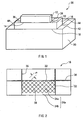
- FIG. 1 shows a construction of a substantial part of the laser diode assembly
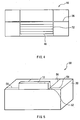
- Fig. 2 shows a construction of grooves of a submount
- Fig. 3 shows a construction of grooves of a heatsink, respectively.
- a laser diode assembly 30 of this embodiment comprises a laser diode device 12, a submount 16 jointed to a substrate side of the laser diode device 12 with a first solder layer 14 in between, and a heatsink 20 jointed to a rear face side of the submount 16 with a second solder layer 18 in between as a substantial part similar to a conventional laser assembly 10.
- the submount 16 comprises a groove 32 (hereinafter referred to as submount groove) and an extension groove 36.
- the submount groove 32 is formed around a joint area 34 along border of the joint area 34 jointed with the laser diode device 12.
- the extension groove 36 is a groove extended from the submount groove 32 to edges of the submount 16.
- the submount groove 32 is formed around the joint area 34 along border of the joint area 34 of the submount 16, which is on both side wall sides and a rear end face side opposite of an emitting end face of the laser diode device 12.
- submount thin grooves 38 whose groove width is smaller and whose groove depth is shallower than of the submount groove 32 are formed so that the submount thin grooves 38 are spaced from each other and at least one ends of the submount thin grooves 38 contact with the submount groove 32.
- the submount thin grooves 38 are formed on the joint area 34 of the submount 16 in the shape of lattice and in the direction diagonally to the submount groove 32.
- the submount groove 32 and the submount thin grooves 38 are not provided on the emitting end face side of the laser diode device 12. That is, the submount groove 32 and the submount thin grooves 38 are closed on the emitting end face side of the laser diode device 12.
- the joint area 34 is composed of a joint area 34a wherein the submount thin grooves 38 are arranged and a joint area 34b which is on the continuous same plane as areas other than the joint area 34, wherein the submount thin grooves 38 are not arranged.
- the heatsink 20 also comprises a groove 42 (hereinafter referred to as heatsink groove) formed around a joint area 40 along border of the joint area 40 of the heatsink 20 wherein the submount 16 and the heatsink 20 are jointed and an extension groove 44 extended from the heatsink groove 42 to edges of the heatsink 20.
- heatsink groove a groove 42 (hereinafter referred to as heatsink groove) formed around a joint area 40 along border of the joint area 40 of the heatsink 20 wherein the submount 16 and the heatsink 20 are jointed and an extension groove 44 extended from the heatsink groove 42 to edges of the heatsink 20.
- the heatsink groove 42 is formed around the joint area 40 along border of the joint area 40 of the heatsink 20, which is on the both side wall sides and the rear end face side opposite of the emitting end face of the laser diode device 12.
- a depth and a width of the submount groove 32, the heatsink groove 42, and the extension grooves 36 and 44 are, for example, from 1 ⁇ m to 1 mm.
- a depth and a width of the submount thin groove 38 is approximately from 1 ⁇ m to several hundred ⁇ m.
- solder might excessively flow, or heat release effect of the submount 16 might be lowered.
- the depth and the width of the submount thin groove 38 are too small, providing the thin grooves becomes ineffective.
- a distance P between the respective submount thin grooves 38 is approximately from 1 ⁇ m to 1-2 mm. It is not preferable that the distance P between the submount thin grooves 38 is less than 1 ⁇ m, since irregularity is too fine and a surface of the joint area 34 becomes a state similar to surface roughness. Further, since an area of the joint area 34 is not so large, providing the submount thin grooves 38 becomes ineffective when the distance P is 2 mm or more.
- the submount 16 when solder joint between the laser diode device 12 and the submount 16 is performed, excessive solder flows into the submount groove 32 through the submount thin grooves 38, the submount groove 32 functions as a solder pool for the excessive solder, and the excessive solder is drained outside through the extension groove 36. Therefore, when the laser diode device 12 and the submount 16 are jointed, bulb-shaped excessive solder never remains around the joint area 34 of the submount 16.
- the submount groove 32 and the submount thin grooves 38 are not provided on the emitting end face side of the laser diode device 12. Therefore, excessive solder never flows onto the emitting end face side of the laser diode device 12.
- the heatsink 20 is provided with the heatsink groove 42 and the extension groove 44. Therefore, when solder joint between the submount 16 and the heatsink 20 is performed, excessive solder flows into the heatsink groove 42, the heatsink groove 42 functions as a solder pool for the excessive solder, and the excessive solder is drained outside through the extension groove 44.
- the submount groove 32 it is not necessary to provide the submount groove 32 over a whole length of border of the joint area 34 depending on sizes or shapes of the joint area 34 of the submount 16. It is possible to partly provide the submount groove 32, for example, only at border on the both side wall sides of the laser diode device 12, or only at border on the rear end face side of the laser diode device 12. In such a case, the extension groove 36 contacts with the partly provided submount groove 32.
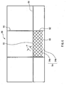
- Fig. 4 shows a construction of submount grooves according to a modification of the laser diode assembly of the first embodiment.
- the submount thin grooves 38 are formed on the joint area 34 of the submount 16 in the shape of lattice and in the direction diagonally to the submount groove 32.
- submount thin grooves 46 are formed on the joint area 34 so that the submount thin grooves 46 are parallel to border of the joint area 34 on the rear end face side of the laser diode device 12.
- thin grooves having a construction similar to of the submount thin grooves can be provided on the joint area 40 of the heatsink 20. It becomes thereby possible that excessive solder further easily flows into the heatsink groove 42 through the thin grooves when solder joint between the submount 16 and the heatsink 20 is performed.
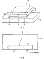
- Fig. 5 shows a construction of a substantial part of a laser diode assembly 50
- Fig. 6 shows a construction of heatsink grooves, respectively.
- the laser diode assembly 50 has the same construction as the conventional laser assembly 10 except that the laser diode device 12 is directly jointed to the heatsink 20 without the foregoing submount 16 in between.
- the heatsink 20 comprises a groove 52 (hereinafter referred to as heatsink groove) and an extension groove 56.
- the heatsink groove 52 is formed around a joint area 54 along border of the joint area 54 jointed with the laser diode device 12.
- the extension groove 56 is extended from the heatsink groove 52 to edges of the heatsink 20.
- the heatsink groove 52 is formed around the joint area 54 along border of the joint area 54 of the heatsink 20 on the both side wall sides and the rear end face side opposite of the emitting end face of the laser diode device 12.
- thin grooves 58 (hereinafter referred to as heatsink thin grooves) whose groove width is smaller and whose groove depth is shallower than of the heatsink groove 52 are formed on the joint area 54 of the heatsink 20 in the shape of lattice and in the direction diagonally to the heatsink groove 52 so that the heatsink thin grooves are spaced from each other and at least one ends of the heatsink thin grooves contact with the heatsink groove 52.
- the heatsink groove 52 and the heatsink thin grooves 58 are not provided on the emitting end face side of the laser diode device 12. That is, the heatsink groove 52 and the heatsink thin grooves 58 are closed on the emitting end face side of the laser diode device 12.
- the joint area 54 is composed of a joint area 54a wherein the heatsink thin grooves 58 are arranged and a joint area 54b which is on the continuous same plane as areas other than the joint area 54, wherein the heatsink thin grooves 58 are not arranged.
- a depth and a width of the heatsink groove 52 and the extension grooves 56 are from 1 ⁇ m to 1 mm.
- a depth and a width of the heatsink thin groove 58 is approximately from 1 ⁇ m to several hundred ⁇ m, considering excessive flow of solder and heat release.
- a distance P between the respective heatsink thin grooves 58 is approximately from 1 ⁇ m to 1-2 mm. It is not preferable that the distance P between the heatsink thin grooves 58 is less than 1 ⁇ m, since a surface of the joint area 54 becomes a state similar to surface roughness. Further, since an area of the joint area 54 is not so large, providing the heatsink thin grooves 58 becomes ineffective when the distance P is 2 mm or more.
- the heatsink groove 52 when solder joint between the laser diode device 12 and the heatsink 20 is performed, excessive solder flows into the heatsink groove 52 through the heatsink thin grooves 58, the heatsink groove 52 functions as a solder pool for the excessive solder, and the excessive solder is drained outside through the extension groove 56.
- the extension groove 56 also has a function as a solder pool for the excessive solder.
- bulb-shaped excessive solder never remains around the joint area 54 of the heatsink 20 when joint between the laser diode device 12 and the heatsink, 20 is performed.
- the joint area of the laser diode device 12 is small, it is possible to provide only the heatsink groove 52. It is not indispensable to provide the submount thin grooves 58.
- the heatsink groove 52 and the heatsink thin grooves 58 are not provided on the emitting end face side of the laser diode device 12. Therefore, excessive solder never flows to the emitting end face side of the laser diode device 12.
- the heatsink groove 52 it is not necessary to provide the heatsink groove 52 over a whole length of border of the joint area 54 depending on sizes or shapes of the joint area 54 of the heatsink 20. It is possible to partly provide the heatsink groove 52, for example, only at border on the both side wall sides of the laser diode device 12, or only at border on the rear end face side of the laser diode device 12. In such a case, the extension groove 56 contacts with the partly provided heatsink groove 52.
- This embodiment relates to a laser diode assembly according to a third example.
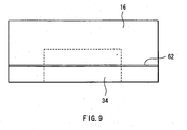
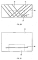
- Fig. 9 shows a construction of a submount groove thereof.
- the laser diode assembly of this embodiment has the same construction as of the laser diode assembly 30 of the first embodiment except that the construction of the submount groove is different.
- the submount 16 comprises one submount transverse groove 62.
- the submount transverse groove 62 crosses the central part of the joint area 34 jointed with the laser diode device 12 (refer to Fig. 1 ) in the direction parallel to the emitting end face of the laser diode device 12 to edges of the submount 16.
- a size of the submount transverse groove 62 is the same as of the submount groove 32 of the first embodiment.
- the submount transverse groove 62 can be plural. Further, it is not indispensable that the submount transverse groove 62 crosses the central part of the joint area 34 of the submount 16.
- the submount transverse groove 62 can cross location of the joint area 34, which is close to the emitting end face.
- bulb-shaped excessive solder never remains around the joint area 34 of the submount 16 when joint between the laser diode device 12 and the submount 16 is performed.
- Fig. 10 shows a construction of a heatsink groove thereof.
- the laser diode assembly of this embodiment is the same as the laser diode assembly 50 of the second embodiment except that the construction of the heatsink groove is different.
- the heatsink 20 comprises a heatsink transverse groove 64.
- the heatsink transverse groove 64 crosses the central part of the joint area 54 jointed with the laser diode device 12 (refer to Fig. 5 ) in the direction parallel to the emitting end face of the laser diode device 12 to edges of the heatsink 20.
- a size of the heatsink transverse groove 64 is the same as of the second heatsink groove 52 of the third embodiment.
- the heatsink transverse groove 62 can be plural. Further, it is not indispensable that the heatsink transverse groove 64 crosses the central part of the joint area 54 of the heatsink 20.
- the heatsink transverse groove 64 can cross location of the joint area 54, which is close to the emitting end face.
- bulb-shaped excessive solder never remains around the joint area 54 of the heatsink 20 when joint between the laser diode device 12 and the heatsink 20 is performed.
- This embodiment relates to a laser diode assembly according to a fifth example.
- Fig. 11 shows a construction of submount grooves thereof.
- the laser diode assembly of this embodiment is the same as the laser diode assembly 30 of the first embodiment except that the construction of the submount grooves is different.
- the submount 16 does not comprise the foregoing submount groove 32 and extension groove 36, but comprises several thin grooves in the joint area 34 jointed with the laser diode device 12 (refer to Fig. 1 ). In this embodiment, only the same thin grooves as the submount thin grooves 38 of the first embodiment are provided.
- the submount 16 comprises the submount thin grooves 38
- excessive solder flows into the submount thin grooves 38
- the submount thin grooves 38 function as a solder pool for the excessive solder when solder joint between the laser diode device 12 and the submount 16 is performed.
- This embodiment relates to a laser diode assembly according to the fifth example.
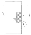
- Fig. 12 shows a construction of heatsink grooves thereof.
- the laser diode assembly of this embodiment is the same as the laser diode assembly 50 of the second embodiment except that the construction of the heatsink grooves is different.
- the heatsink 20 does not comprise the second heatsink groove 52 and the extension groove 56, but comprises several thin grooves in the joint area 54 jointed with the laser diode device 12 (refer to Fig. 1 ). In this embodiment, only the same thin grooves as the heatsink thin grooves 58 of the second embodiment are provided.
- solder can be stably set while good flatness of the joint area 34 of the submount 16 and the joint area 54 of the heatsink 20 is maintained. Therefore, air entrance between solder and the joint area, or deterioration of contact characteristics between the joint area and solder can be prevented.
- This embodiment relates to a laser diode assembly according to a seventh example.
- Fig. 14 shows a construction of a submount transverse groove thereof.
- the laser diode assembly of this embodiment has the same construction as of the laser diode assembly 30 of the first embodiment except that the groove construction of the submount 16 is different.
- the submount 16 comprises one submount transverse groove 65.
- the submount transverse groove 65 crosses the central part of the joint area 34 jointed with the laser diode device 12 (refer to Fig. 1 ), and extends in the direction parallel to the emitting end face of the laser diode device 12.
- the submount transverse groove 65 is closed at its both ends. As long as excessive solder melt can be pooled, it is not necessary to extend the submount transverse groove 65 to the edges of the submount 16 as the submount transverse groove 62 of the third embodiment.
- a shape of the submount transverse groove 65 is flexible.
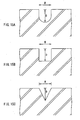
- the submount transverse groove 65 can be a U groove as shown in Fig. 15A .
- a cross section of the submount transverse groove 65 can be rectangle
- a cross section of the submount transverse groove 65 can be triangle.
- each width W and depth D shown in Figs. 15A to 15C is from 1 ⁇ m to 1 mm, and preferably from several dozen ⁇ m to 300 ⁇ m.
- the submount transverse groove 65 is the U groove whose width W and depth D are 150 ⁇ m, respectively.
- solder joint between the laser diode device 12 and the submount 16 when solder joint between the laser diode device 12 and the submount 16 is performed, excessive solder drains into the submount transverse groove 65 and flows inside the submount transverse groove 65 due to capillary thereof, and the submount transverse groove 65 functions as a solder pool for the excessive solder.
- This embodiment relates to a laser diode assembly according to the seventh example.
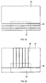
- Fig. 16 shows a construction of submount transverse grooves thereof.
- the laser diode assembly of this embodiment has the same construction as of the laser diode assembly 30 of the first embodiment except that the groove construction of the submount 16 is different.
- the submount 16 has several (three in this embodiment) submount transverse grooves 66.
- the submount transverse grooves 66 cross the central part of the joint area 34 jointed with the laser diode device 12 (refer to Fig. 1 ), and cross from one edge to the other facing edge of the submount 16 in the direction parallel to the emitting end face of the laser diode device 12.
- An arrangement pitch of the submount transverse grooves 66 is about 1 mm.
- a shape and a size of the submount transverse groove 66 are the same as of the submount transverse groove 65 of the seventh embodiment.
- the pitch varies depending on solder amounts. When the pitch is small, it becomes difficult to maintain flatness in the process.
- the pitch is basically approximately from several hundred ⁇ m to 2 mm.
- the submount transverse grooves 66 function as a solder pool for the excessive solder, and the excessive solder is drained outside.
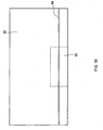
- Fig. 17 shows a construction of a submount transverse groove thereof.
- the laser diode assembly of this embodiment has the same construction as of the laser diode assembly 30 of the first embodiment except that the groove construction of the submount 16 is different.
- the submount 16 has one submount transverse groove 68.
- the submount transverse groove 68 crosses the central part of the joint area 34 jointed with the laser diode device 12 (refer to Fig. 1 ), and extends from one edge to the other facing edge of the submount 16 in the direction parallel to the emitting end face of the laser diode device 12.
- the submount 16 has several submount branch grooves 70.
- One ends of the submount branch grooves 70 contact with the submount transverse groove 68, and the other ends of the submount branch grooves 70 extend to the edge opposite of the emitting end face side of the laser diode device 12 in the direction perpendicular to the submount transverse groove 68.
- An arrangement pitch of the submount branch grooves 70 is about 1 mm.
- a shape and a size of the submount transverse groove 68 and the submount branch groove 70 are the same as of the submount transverse groove 65 of the seventh embodiment.
- the submount branch grooves 70 are provided in addition to the submount transverse groove 68. Therefore, when solder joint between the laser diode device 12 and the submount 16 is performed, excessive solder flows from the submount transverse groove 68 into the submount branch grooves 70, the excessive solder flows in the submount transverse groove 68 and the submount branch grooves 70 due to capillary phenomenon in the submount transverse groove 68 and the submount branch grooves 70, the submount transverse groove 68 and the submount branch grooves 70 function as a solder pool for the excessive solder, and the excessive solder is drained outside through the submount branch grooves 70.
- the submount branch grooves 70 extend in the direction perpendicular to the submount transverse groove 68.
- the extending direction is in the direction perpendicular to the submount transverse groove 68.
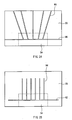
- submount branch grooves 72 can extend to the edge opposite of the emitting end face side in the fan-like shape.
- the submount transverse groove 68 extends from one submount face to the other facing submount face.
- both ends of the submount transverse groove 74 can be closed.
- only one end of the submount transverse groove can be closed.
- one ends of the submount branch grooves 70 extend to the edge opposite of the emitting end face side of the laser diode device in the direction perpendicular to the transverse groove 68.
- the submount branch grooves have enough groove capacities as a solder pool for the excessive solder, as shown in Fig. 18 , the other ends can be closed.
- This embodiment relates to a laser diode assembly according to the seventh example.
- Fig. 20 shows a construction of submount transverse grooves thereof.
- the laser diode assembly of this embodiment has the same construction as of the laser diode assembly 30 of the first embodiment except that the groove construction of the submount 16 is different.
- the submount 16 has several first submount cross grooves 78 and second submount cross grooves 80.
- the first submount cross grooves 78 cross the joint area 34 jointed with the laser diode device 12 (refer to Fig. 1 ) at a crossing angle ⁇ 1 of 40° in relation to an edge of the submount 16 on the emitting end face side of the laser diode device 12.
- the second submount cross grooves 80 cross the joint area 34 at a crossing angle ⁇ 2 of 140°.
- the crossing angle ⁇ 2 its clockwise crossing angle is 40°.
- An arrangement pitch of the first submount cross grooves 78 and the second submount cross grooves 80 is about 1 mm.
- a shape and a size thereof are the same as of the submount transverse groove 65 of the seventh embodiment.
- the first submount cross grooves 78 and the second submount cross grooves 80 are provided. Therefore, when solder joint between the laser diode device 12 and the submount 16 is performed, excessive solder flows into these grooves, the excessive solder flows in these grooves due to capillary phenomenon in these grooves, these grooves function as a solder pool for the excessive solder, and the excessive solder is drained outside.
- the first submount cross grooves 78 and the second submount cross grooves 80 extend to the submount face on the emitting end face side of the laser diode device 12.
- the crossing angles ⁇ 1 and ⁇ 2 are respectively in the angle range specified in the invention. Therefore, solder melt never flows to the submount face on the emitting end face side.
- crossing angles ⁇ 1 and ⁇ 2 are flexible as long as they are 45° or less in relation to the submount face on the emitting end face side.
- Fig. 21 shows a construction of a heatsink groove thereof.
- the laser diode assembly of this embodiment has the same construction as of the laser diode assembly 50 of the second embodiment except that the groove construction of the heatsink 20 is different.
- the heatsink 20 has one heatsink transverse groove 82.
- the heatsink transverse groove 82 crosses the central part of the joint area 54 jointed with the laser diode device 12 (refer to Fig. 1 ), and extends in the direction parallel to the emitting end face of the laser diode device 12.
- this heatsink transverse groove 82 is closed at its both ends. As long as excessive solder melt can be pooled, it is not necessary to extend the heatsink transverse groove to the edges of the heatsink 20 as the heatsink transverse groove 64 of the fourth embodiment.
- Fig. 22 shows a construction of heatsink transverse grooves thereof.
- the laser diode assembly of this embodiment has the same construction as of the laser diode assembly 50 of the second embodiment except that the groove construction of the heatsink 20 is different.
- the heatsink 20 has several (three in this embodiment) heatsink transverse grooves 84.
- the heatsink transverse grooves 84 cross the central part of the joint area 54 jointed with the laser diode device 12 (refer to Fig. 1 ) from one edge to the other facing edge of the heatsink 20 in the direction parallel to the emitting end face of the laser diode device 12.
- An arrangement pitch of the heatsink transverse grooves 84 is about 1 mm.
- a shape and a size of the heatsink transverse groove 84 are the same as of the submount transverse groove 65 of the seventh embodiment.
- Fig. 23 shows a construction of a heatsink transverse groove thereof.
- the laser diode assembly of this embodiment has the same construction as of the laser diode assembly 50 of the second embodiment except that the groove construction of the heatsink 20 is different.
- the heatsink 20 has one heatsink transverse groove 86.
- the heatsink transverse groove 86 crosses the central part of the joint area 54 jointed with the laser diode device 12 (refer to Fig. 1 ), and extends from one edge to the other facing edge of the heatsink 20 in the direction parallel to the emitting end face of the laser diode device 12.
- the heatsink 20 comprises several heatsink branch grooves 88.
- One ends of the heatsink branch grooves 88 contact with the heatsink transverse groove 86, and the other ends of the heatsink branch grooves 88 extend to the edge opposite of the emitting end face side of the laser diode device in the direction perpendicular to the heatsink transverse groove 86.
- An arrangement pitch of the heatsink branch grooves 88 is about 1 mm.
- a shape and a size of the heatsink transverse groove 86 and the heatsink branch groove 88 is the same as of the submount transverse groove 65 of the seventh embodiment.
- the heatsink branch grooves 88 extend in the direction perpendicular to the heatsink transverse groove 86.
- it is not indispensable that the extending direction is in the direction perpendicular to the heatsink transverse groove 86.
- heatsink branch grooves 90 can extend to the edge opposite of the emitting end face side in the fan-like shape.
- the heatsink transverse groove 86 extends from one heatsink face to the other facing heatsink face.
- both ends of a heatsink transverse groove 92 can be closed.
- only one end of the heatsink transverse groove can be closed.
- other ends of the heatsink branch grooves 88 extend to the edge opposite of the emitting end face side of the laser diode device in the direction perpendicular to the heatsink transverse groove 86.
- branch grooves have enough groove capacities as a solder pool for the excessive solder, as shown in Fig 25 , the other ends of heatsink branch grooves 94 can be closed.
- Fig. 26 shows a construction of heatsink transverse grooves thereof.
- the laser diode assembly of this embodiment is the same as the laser diode assembly 50 of the second embodiment except that the groove construction of the heatsink 20 is different.
- the heatsink 20 has several first heatsink cross grooves' 96 and several second heatsink cross grooves 98.
- the first heatsink cross grooves 96 cross the joint area 54 jointed with the laser diode device 12 (refer to Fig. 1 ) at a crossing angle ⁇ 1 of 40° in relation to an edge of the heatsink 20 on the emitting end face side of the laser diode device 12.
- the second heatsink cross grooves 98 cross the joint area 54 at a crossing angle ⁇ 2 of 140°.
- An arrangement pitch of the first heatsink cross grooves 96 and the second heatsink cross grooves 98 is about 1 mm.
- a shape and a size thereof are the same as of the submount transverse groove 65 of the seventh embodiment.
- the first heatsink cross grooves 96 and the second heatsink cross grooves 98 extend to the heatsink face on the emitting end face side of the laser diode device 12.
- the crossing angles ⁇ 1 and ⁇ 2 are respectively in the angle range specified in the invention. Therefore, solder melt never flows to the heatsink face on the emitting end face side.
- crossing angles ⁇ 1 and ⁇ 2 are flexible as long as they are 45° or less in relation to the heatsink face on the emitting end face side.
- This embodiment relates to a method of manufacturing a laser diode assembly according to a ninth example. This embodiment is applied to manufacturing the laser diode assembly of the seventh embodiment.
- the submount 16 which holds the laser diode device 12 on the joint area 34 of the submount 16 is forwarded in a reflow oven, and solder on the joint area 34 of the submount 16 is melted.
- the submount 16 on which the laser diode 12 is fixed is taken out of the reflow oven.
- the heatsink 20 which holds the submount 16 on the joint area 54 of the heatsink 20 is forwarded in the reflow oven, and solder on the joint area 54 of the heatsink 20 is melted. Excessive solder out of the melted solder is drained out between the heatsink 20 and the submount 16, flown and pooled in the heatsink transverse groove due to capillary phenomenon arising in the heatsink transverse groove which crosses the joint area 54 of the heatsink 20.
- the submount 16 is jointed to the heatsink 20.
- joint between the laser diode device 12 and the submount 16 and joint between the submount 16 and the heatsink 20 can be concurrently performed in the reflow oven.
- a method of manufacturing the laser diode assembly according to the tenth example can be performed in a manner similar to in this embodiment basically.
- the submount groove is provided; and in the second invention, when solder joint between the laser diode device and the heatsink is performed, the second heatsink groove is provided. Excessive solder is thereby drained out into the submount groove or the second heatsink groove, the submount groove or the second heatsink groove functions as a solder pool for the excessive solder, and the excessive solder is drained outside. Therefore, bulb-shaped excessive solder never remains around the joint area between the laser diode device and the submount, and the joint area between the laser diode device and the heatsink.
- solder is stably set while good flatness of the joint area is maintained. Therefore, air entrance between solder and the joint area, or deterioration of contact characteristics between the joint area and solder can be prevented.
- the submount transverse groove is provided.
- the heatsink transverse groove is provided. Excessive solder is thereby drained out into the submount transverse groove or the heatsink transverse groove, the submount transverse groove or the heatsink transverse groove functions as a solder pool for the excessive solder, and the excessive solder is drained outside. Therefore, bulb-shaped excessive solder never remains around the joint area between the laser diode device and the submount and the joint area between the laser diode device and the heatsink.
- solder is stably set while good flatness of the joint area is maintained. Therefore, air entrance between solder and the joint area, or deterioration of contact characteristics between the joint area and solder can be prevented.
- the thin grooves are provided on the joint area of the submount.
- the thin grooves are provided on the joint area of the heatsink. Excessive solder is thereby drained out into the thin grooves, and the thin grooves function as a solder pool for the excessive solder. Therefore, bulb-shaped excessive solder never remains around the joint area between the laser diode device and the submount, and the joint area between the laser diode device and the heatsink.
- solder is stably set while good flatness of the joint area is maintained. Therefore, air entrance between solder and the joint area, or deterioration of contact characteristics between the joint area and solder can be prevented.
- the various modes of the submount transverse groove are provided.
- the various modes of the heatsink transverse groove are provided. Excessive solder is thereby drained out into the submount transverse groove or the heatsink transverse groove, the submount transverse groove or the heatsink transverse groove functions as a solder pool for the excessive solder, and the excessive solder is drained outside due to capillary phenomenon in the submount transverse groove or the heatsink transverse groove.
- bulb-shaped excessive solder never remains around the joint area between the laser diode device and the submount, and the joint area between the laser diode device and the heatsink.
Landscapes
- Physics & Mathematics (AREA)
- Condensed Matter Physics & Semiconductors (AREA)
- General Physics & Mathematics (AREA)
- Electromagnetism (AREA)
- Optics & Photonics (AREA)
- Semiconductor Lasers (AREA)
- Cooling Or The Like Of Semiconductors Or Solid State Devices (AREA)
Claims (5)
- Ensemble de diode laser comportant : un dispositif de diode laser ; une embase articulée sur le dispositif de diode laser avec une première couche de soudure entre eux, et un élément de dissipation thermique articulé sur un côté postérieur de l'embase avec une seconde couche de soudure entre eux,
dans lequel l'embase présente une rainure d'embase au moins en une partie d'une périphérie d'une zone d'articulation le long d'une bordure de la zone d'articulation articulée avec le dispositif de diode laser, et plusieurs rainures minces de l'embase, dont la largeur est inférieure et la profondeur est moindre que celles de la rainure de l'embase, sont formées sur la zone d'articulation de l'embase de sorte que les rainures minces de l'embase sont espacées les unes des autres, et au moins une des extrémités des rainures minces de l'embase est en contact avec la rainure de l'embase. - Ensemble de diode laser selon la revendication 1, dans lequel l'élément de dissipation thermique présente une rainure d'élément de dissipation thermique à une périphérie d'une zone d'articulation le long d'une bordure de la zone d'articulation articulée avec l'embase.
- Ensemble de diode laser selon la revendication 1, dans lequel la rainure de l'embase est formée le long de la bordure de la zone d'articulation de l'embase sur une surface terminale postérieure à l'opposé d'une surface terminale d'émission du dispositif de diode laser et de la bordure de la zone d'articulation de l'embase sur les deux côtés de parois latérales du dispositif de diode laser.
- Ensemble de diode laser selon la revendication 1, dans lequel les rainures minces de l'embase s'étendent en diagonale par rapport à la rainure de l'embase, ou parallèlement à la bordure de la zone d'articulation sur la surface terminale postérieure du dispositif de diode laser.
- Ensemble de diode laser selon la revendication 4, dans lequel des orifices de sortie correspondants à la surface terminale d'émission du dispositif de diode laser de la gorge de l'embase et des gorges minces de l'embase sont fermés.
Applications Claiming Priority (5)
| Application Number | Priority Date | Filing Date | Title |
|---|---|---|---|
| JP2002376591 | 2002-12-26 | ||
| JP2002376591 | 2002-12-26 | ||
| JP2003163383 | 2003-06-09 | ||
| JP2003163383 | 2003-06-09 | ||
| PCT/JP2003/016946 WO2004077630A1 (fr) | 2002-12-26 | 2003-12-26 | Ensemble laser a semi-conducteur |
Publications (3)
| Publication Number | Publication Date |
|---|---|
| EP1577992A1 EP1577992A1 (fr) | 2005-09-21 |
| EP1577992A4 EP1577992A4 (fr) | 2006-01-11 |
| EP1577992B1 true EP1577992B1 (fr) | 2008-11-26 |
Family
ID=32929620
Family Applications (1)
| Application Number | Title | Priority Date | Filing Date |
|---|---|---|---|
| EP03786367A Expired - Lifetime EP1577992B1 (fr) | 2002-12-26 | 2003-12-26 | Ensemble laser a semi-conducteur |
Country Status (6)
| Country | Link |
|---|---|
| US (1) | US7502397B2 (fr) |
| EP (1) | EP1577992B1 (fr) |
| JP (1) | JP4626517B2 (fr) |
| DE (1) | DE60324962D1 (fr) |
| TW (1) | TWI258258B (fr) |
| WO (1) | WO2004077630A1 (fr) |
Families Citing this family (27)
| Publication number | Priority date | Publication date | Assignee | Title |
|---|---|---|---|---|
| KR20060115453A (ko) * | 2005-05-06 | 2006-11-09 | 삼성전자주식회사 | 방열 구조체 및 이를 구비한 발광소자 조립체 |
| JP4765408B2 (ja) * | 2005-05-31 | 2011-09-07 | ソニー株式会社 | 半導体レーザ装置並びに放熱部材および支持部材 |
| JP4846515B2 (ja) * | 2006-10-18 | 2011-12-28 | 株式会社東芝 | 光半導体装置及び光半導体装置の製造方法 |
| WO2009084112A1 (fr) * | 2007-12-28 | 2009-07-09 | Mitsubishi Electric Corporation | Dispositif source de lumière laser |
| CN101959389B (zh) * | 2009-07-13 | 2014-07-16 | 富瑞精密组件(昆山)有限公司 | 散热装置及其制造方法 |
| JP2012119637A (ja) | 2010-12-03 | 2012-06-21 | Sumitomo Electric Device Innovations Inc | 光半導体装置の製造方法 |
| US8456961B1 (en) | 2011-03-22 | 2013-06-04 | Western Digital (Fremont), Llc | Systems and methods for mounting and aligning a laser in an electrically assisted magnetic recording assembly |
| US8518748B1 (en) | 2011-06-29 | 2013-08-27 | Western Digital (Fremont), Llc | Method and system for providing a laser submount for an energy assisted magnetic recording head |
| US8288204B1 (en) | 2011-08-30 | 2012-10-16 | Western Digital (Fremont), Llc | Methods for fabricating components with precise dimension control |
| US8665677B1 (en) | 2011-12-19 | 2014-03-04 | Western Digital (Fremont), Llc | Disk drive magnetic read head with affixed and recessed laser device |
| US8773664B1 (en) | 2011-12-20 | 2014-07-08 | Western Digital (Fremont), Llc | Method and system for aligning substrates for direct laser coupling in an energy assisted magnetic recording head |
| US8879593B2 (en) * | 2012-03-16 | 2014-11-04 | The United States Of America, As Represented By The Secretary Of The Navy | Epitaxial-side-down mounted high-power semiconductor lasers |
| US9475151B1 (en) | 2012-10-30 | 2016-10-25 | Western Digital (Fremont), Llc | Method and apparatus for attaching a laser diode and a slider in an energy assisted magnetic recording head |
| US9431037B2 (en) | 2013-03-12 | 2016-08-30 | Western Digitatl (Fremont), LLC | Systems and methods for monitoring the power of a light source utilized in energy-assisted magnetic recording |
| JP5652494B2 (ja) * | 2013-03-29 | 2015-01-14 | ウシオ電機株式会社 | 半導体レーザ装置 |
| US8897102B1 (en) | 2013-04-02 | 2014-11-25 | Western Digital (Fremont), Llc | Method and system for measuring light delivery offsets in a heat assisted magnetic recording head |
| US9001628B1 (en) | 2013-12-16 | 2015-04-07 | Western Digital (Fremont), Llc | Assistant waveguides for evaluating main waveguide coupling efficiency and diode laser alignment tolerances for hard disk |
| DE102014012855A1 (de) * | 2014-09-03 | 2015-10-01 | Jenoptik Laser Gmbh | Diodenlaser und Herstellungsverfahren für einen Diodenlaser |
| US9042048B1 (en) | 2014-09-30 | 2015-05-26 | Western Digital (Fremont), Llc | Laser-ignited reactive HAMR bonding |
| US9902023B1 (en) | 2014-10-28 | 2018-02-27 | Western Digital (Fremont), Llc | Systems and devices for achieving high throughput attachment and sub-micron alignment of components |
| US9257138B1 (en) | 2014-10-28 | 2016-02-09 | Western Digital (Fremont), Llc | Slider assembly and method of manufacturing same |
| JP6439389B2 (ja) * | 2014-11-05 | 2018-12-19 | 富士電機株式会社 | 半導体装置 |
| US10044171B2 (en) * | 2015-01-27 | 2018-08-07 | TeraDiode, Inc. | Solder-creep management in high-power laser devices |
| US9171562B1 (en) | 2015-03-19 | 2015-10-27 | Western Digital (Fremont), Llc | Patterned metal layer to control solder connection between laser and submount in a magnetic head |
| CN106848831A (zh) * | 2017-04-10 | 2017-06-13 | 海信集团有限公司 | 一种to激光器支架 |
| TWI674375B (zh) * | 2019-03-15 | 2019-10-11 | 聯鈞光電股份有限公司 | 發光裝置及其製作方法 |
| JP7478643B2 (ja) * | 2020-10-22 | 2024-05-07 | 新光電気工業株式会社 | 回路基板 |
Family Cites Families (22)
| Publication number | Priority date | Publication date | Assignee | Title |
|---|---|---|---|---|
| JPS6018985A (ja) * | 1983-07-13 | 1985-01-31 | Hitachi Ltd | 発光装置 |
| DE3733849C1 (de) * | 1987-10-07 | 1989-05-11 | Franz Arnold | Maschinenschraubstock mit Kraftverstaerker |
| JPH01127275U (fr) * | 1988-02-24 | 1989-08-31 | ||
| JPH0272573U (fr) * | 1988-11-18 | 1990-06-01 | ||
| JPH03217065A (ja) * | 1990-01-23 | 1991-09-24 | Toshiba Corp | レーザダイオード装置 |
| JP3030442B2 (ja) | 1990-08-15 | 2000-04-10 | 御芳 中川 | 遠隔溶射用のアーク溶射装置 |
| JPH0499858U (fr) * | 1991-02-06 | 1992-08-28 | ||
| JPH04352377A (ja) * | 1991-05-29 | 1992-12-07 | Mitsubishi Electric Corp | 半導体レーザ素子用サブマウント |
| JPH0811858B2 (ja) * | 1991-07-10 | 1996-02-07 | 有限会社熱田産業 | 横編み機における仕掛かり装置 |
| JPH0511470U (ja) * | 1991-07-24 | 1993-02-12 | 日本航空電子工業株式会社 | 半導体レーザ用ヒートシンク |
| JPH0525756U (ja) * | 1991-09-13 | 1993-04-02 | 日本航空電子工業株式会社 | ヒートシンク付半導体レーザ |
| JPH06350202A (ja) * | 1993-06-10 | 1994-12-22 | Toshiba Corp | 半導体発光装置 |
| JPH0738208A (ja) * | 1993-07-22 | 1995-02-07 | Nec Corp | 半導体レーザ装置 |
| US5785754A (en) * | 1994-11-30 | 1998-07-28 | Sumitomo Electric Industries, Ltd. | Substrate, semiconductor device, element-mounted device and preparation of substrate |
| DE19701680C2 (de) * | 1997-01-18 | 2001-08-02 | Fraunhofer Ges Forschung | Diamantkörper |
| DE19708472C2 (de) * | 1997-02-20 | 1999-02-18 | Atotech Deutschland Gmbh | Herstellverfahren für chemische Mikroreaktoren |
| US6670222B1 (en) * | 1997-06-14 | 2003-12-30 | Jds Uniphase Corporation | Texturing of a die pad surface for enhancing bonding strength in the surface attachment |
| US6327289B1 (en) * | 1997-09-02 | 2001-12-04 | Matsushita Electric Industrial Co., Ltd. | Wavelength-variable semiconductor laser, optical integrated device utilizing the same, and production method thereof |
| DE10011892A1 (de) * | 2000-03-03 | 2001-09-20 | Jenoptik Jena Gmbh | Montagesubstrat und Wärmesenke für Hochleistungsdiodenlaserbarren |
| JP2001298237A (ja) * | 2000-04-14 | 2001-10-26 | Nippon Telegr & Teleph Corp <Ntt> | 半導体光素子搭載用キャリア、半導体光素子モジュール、およびその製造方法 |
| JP4494587B2 (ja) * | 2000-05-11 | 2010-06-30 | 古河電気工業株式会社 | 光半導体素子用パッケージおよび前記パッケージを用いた光半導体素子モジュール |
| JP2002076373A (ja) * | 2000-08-25 | 2002-03-15 | Fujitsu Ltd | 電子装置及び光学装置 |
-
2003
- 2003-12-26 TW TW092137136A patent/TWI258258B/zh not_active IP Right Cessation
- 2003-12-26 EP EP03786367A patent/EP1577992B1/fr not_active Expired - Lifetime
- 2003-12-26 WO PCT/JP2003/016946 patent/WO2004077630A1/fr not_active Ceased
- 2003-12-26 JP JP2005515867A patent/JP4626517B2/ja not_active Expired - Fee Related
- 2003-12-26 DE DE60324962T patent/DE60324962D1/de not_active Expired - Lifetime
- 2003-12-26 US US10/505,720 patent/US7502397B2/en not_active Expired - Fee Related
Also Published As
| Publication number | Publication date |
|---|---|
| JPWO2004077630A1 (ja) | 2006-06-08 |
| JP4626517B2 (ja) | 2011-02-09 |
| EP1577992A4 (fr) | 2006-01-11 |
| US20050094687A1 (en) | 2005-05-05 |
| US7502397B2 (en) | 2009-03-10 |
| TWI258258B (en) | 2006-07-11 |
| EP1577992A1 (fr) | 2005-09-21 |
| WO2004077630A1 (fr) | 2004-09-10 |
| DE60324962D1 (de) | 2009-01-08 |
| TW200427162A (en) | 2004-12-01 |
Similar Documents
| Publication | Publication Date | Title |
|---|---|---|
| EP1577992B1 (fr) | Ensemble laser a semi-conducteur | |
| CN100409443C (zh) | 含侧向电气连接的半导体管芯的半导体管芯封装 | |
| US7221045B2 (en) | Flat chip semiconductor device and manufacturing method thereof | |
| US6049125A (en) | Semiconductor package with heat sink and method of fabrication | |
| JP6086055B2 (ja) | 半導体装置 | |
| US20030092253A1 (en) | Method of manufacturing semiconductor device | |
| JP2009516389A (ja) | リードフレーム及びクリップを使用する半導体ダイ・パッケージ、並びに製造方法 | |
| US7364063B2 (en) | Thermally coupling an integrated heat spreader to a heat sink base | |
| KR20030091865A (ko) | 반도체 장치 및 반도체 모듈 | |
| US20200279801A1 (en) | Foil-based package with distance compensation | |
| KR20220017759A (ko) | 솔더링 구조 및 이를 갖는 파워 모듈 | |
| KR100603880B1 (ko) | 냉각 수단을 포함하는 전력 전자 소자 | |
| US20250183125A1 (en) | Electronic device and method for manufacturing electronic device | |
| CN107527883A (zh) | 半导体装置及其制造方法以及导电柱 | |
| JP4916241B2 (ja) | 半導体装置及びその製造方法 | |
| US12349299B2 (en) | Electric circuit board and power module | |
| US20200312735A1 (en) | Cooling of electronic devices | |
| JP2000286289A (ja) | 金属貼付基板および半導体装置 | |
| CN104701190A (zh) | 制造腔向下制作载体的系统和方法 | |
| CN100449889C (zh) | 激光二极管装置 | |
| US9171812B1 (en) | Semiconductor device having conductive pads with neck-down portions to prevent solder reflow | |
| US9601405B2 (en) | Semiconductor package with an enhanced thermal pad | |
| US20050269689A1 (en) | Conductor device and method of manufacturing thereof | |
| KR102039791B1 (ko) | 반도체칩 실장방법 및 반도체칩 패키지 | |
| KR102036343B1 (ko) | 광소자용 기판, 광소자 패키지, 광소자용 기판의 제조방법 및 광소자 패키지의 제조방법 |
Legal Events
| Date | Code | Title | Description |
|---|---|---|---|
| PUAI | Public reference made under article 153(3) epc to a published international application that has entered the european phase |
Free format text: ORIGINAL CODE: 0009012 |
|
| 17P | Request for examination filed |
Effective date: 20040823 |
|
| AK | Designated contracting states |
Kind code of ref document: A1 Designated state(s): AT BE BG CH CY CZ DE DK EE ES FI FR GB GR HU IE IT LI LU MC NL PT RO SE SI SK TR |
|
| A4 | Supplementary search report drawn up and despatched |
Effective date: 20051125 |
|
| RBV | Designated contracting states (corrected) |
Designated state(s): DE FR GB |
|
| 17Q | First examination report despatched |
Effective date: 20060309 |
|
| GRAP | Despatch of communication of intention to grant a patent |
Free format text: ORIGINAL CODE: EPIDOSNIGR1 |
|
| GRAS | Grant fee paid |
Free format text: ORIGINAL CODE: EPIDOSNIGR3 |
|
| GRAA | (expected) grant |
Free format text: ORIGINAL CODE: 0009210 |
|
| AK | Designated contracting states |
Kind code of ref document: B1 Designated state(s): DE FR GB |
|
| REG | Reference to a national code |
Ref country code: GB Ref legal event code: FG4D |
|
| REF | Corresponds to: |
Ref document number: 60324962 Country of ref document: DE Date of ref document: 20090108 Kind code of ref document: P |
|
| PLBE | No opposition filed within time limit |
Free format text: ORIGINAL CODE: 0009261 |
|
| STAA | Information on the status of an ep patent application or granted ep patent |
Free format text: STATUS: NO OPPOSITION FILED WITHIN TIME LIMIT |
|
| 26N | No opposition filed |
Effective date: 20090827 |
|
| REG | Reference to a national code |
Ref country code: GB Ref legal event code: 746 Effective date: 20120703 |
|
| REG | Reference to a national code |
Ref country code: DE Ref legal event code: R084 Ref document number: 60324962 Country of ref document: DE Effective date: 20120614 |
|
| PGFP | Annual fee paid to national office [announced via postgrant information from national office to epo] |
Ref country code: GB Payment date: 20121220 Year of fee payment: 10 |
|
| PGFP | Annual fee paid to national office [announced via postgrant information from national office to epo] |
Ref country code: DE Payment date: 20121220 Year of fee payment: 10 Ref country code: FR Payment date: 20130130 Year of fee payment: 10 |
|
| REG | Reference to a national code |
Ref country code: DE Ref legal event code: R119 Ref document number: 60324962 Country of ref document: DE |
|
| GBPC | Gb: european patent ceased through non-payment of renewal fee |
Effective date: 20131226 |
|
| REG | Reference to a national code |
Ref country code: FR Ref legal event code: ST Effective date: 20140829 |
|
| REG | Reference to a national code |
Ref country code: DE Ref legal event code: R119 Ref document number: 60324962 Country of ref document: DE Effective date: 20140701 |
|
| PG25 | Lapsed in a contracting state [announced via postgrant information from national office to epo] |
Ref country code: DE Free format text: LAPSE BECAUSE OF NON-PAYMENT OF DUE FEES Effective date: 20140701 |
|
| PG25 | Lapsed in a contracting state [announced via postgrant information from national office to epo] |
Ref country code: FR Free format text: LAPSE BECAUSE OF NON-PAYMENT OF DUE FEES Effective date: 20131231 Ref country code: GB Free format text: LAPSE BECAUSE OF NON-PAYMENT OF DUE FEES Effective date: 20131226 |