EP1598663B1 - Procédé et appareil d'analyse aux rayons X avec un Réseau de détecteurs bidemensionnel - Google Patents
Procédé et appareil d'analyse aux rayons X avec un Réseau de détecteurs bidemensionnel Download PDFInfo
- Publication number
- EP1598663B1 EP1598663B1 EP05009958A EP05009958A EP1598663B1 EP 1598663 B1 EP1598663 B1 EP 1598663B1 EP 05009958 A EP05009958 A EP 05009958A EP 05009958 A EP05009958 A EP 05009958A EP 1598663 B1 EP1598663 B1 EP 1598663B1
- Authority
- EP
- European Patent Office
- Prior art keywords
- detector
- data set
- pixel
- data sets
- source
- Prior art date
- Legal status (The legal status is an assumption and is not a legal conclusion. Google has not performed a legal analysis and makes no representation as to the accuracy of the status listed.)
- Expired - Lifetime
Links
- 238000000034 method Methods 0.000 title claims description 44
- 238000002441 X-ray diffraction Methods 0.000 title claims description 28
- 238000006073 displacement reaction Methods 0.000 claims description 20
- 238000005259 measurement Methods 0.000 claims description 11
- 238000011156 evaluation Methods 0.000 claims description 10
- 230000005855 radiation Effects 0.000 claims description 10
- 230000035945 sensitivity Effects 0.000 claims description 7
- 238000009826 distribution Methods 0.000 claims description 6
- 238000001514 detection method Methods 0.000 claims description 5
- 238000001228 spectrum Methods 0.000 claims description 4
- 239000004020 conductor Substances 0.000 claims description 2
- 230000000737 periodic effect Effects 0.000 claims description 2
- 229920001721 polyimide Polymers 0.000 claims description 2
- 238000011835 investigation Methods 0.000 claims 2
- 239000004642 Polyimide Substances 0.000 claims 1
- 230000002950 deficient Effects 0.000 description 16
- 230000000694 effects Effects 0.000 description 6
- 230000003287 optical effect Effects 0.000 description 4
- 238000011161 development Methods 0.000 description 3
- 238000005457 optimization Methods 0.000 description 3
- 239000004065 semiconductor Substances 0.000 description 3
- 208000012886 Vertigo Diseases 0.000 description 2
- 238000003384 imaging method Methods 0.000 description 2
- 230000002452 interceptive effect Effects 0.000 description 2
- 238000004519 manufacturing process Methods 0.000 description 2
- 230000009467 reduction Effects 0.000 description 2
- 229910004613 CdTe Inorganic materials 0.000 description 1
- 229910001218 Gallium arsenide Inorganic materials 0.000 description 1
- 241000220317 Rosa Species 0.000 description 1
- 238000003491 array Methods 0.000 description 1
- 238000004364 calculation method Methods 0.000 description 1
- 230000008859 change Effects 0.000 description 1
- 239000002131 composite material Substances 0.000 description 1
- 238000010276 construction Methods 0.000 description 1
- 238000013461 design Methods 0.000 description 1
- 238000005516 engineering process Methods 0.000 description 1
- 230000036541 health Effects 0.000 description 1
- 230000006872 improvement Effects 0.000 description 1
- 239000000463 material Substances 0.000 description 1
- 230000005433 particle physics related processes and functions Effects 0.000 description 1
- 238000012545 processing Methods 0.000 description 1
- 238000011160 research Methods 0.000 description 1
- 230000008054 signal transmission Effects 0.000 description 1
- 239000010409 thin film Substances 0.000 description 1
Images

Classifications
-
- G—PHYSICS
- G01—MEASURING; TESTING
- G01N—INVESTIGATING OR ANALYSING MATERIALS BY DETERMINING THEIR CHEMICAL OR PHYSICAL PROPERTIES
- G01N23/00—Investigating or analysing materials by the use of wave or particle radiation, e.g. X-rays or neutrons, not covered by groups G01N3/00 – G01N17/00, G01N21/00 or G01N22/00
- G01N23/20—Investigating or analysing materials by the use of wave or particle radiation, e.g. X-rays or neutrons, not covered by groups G01N3/00 – G01N17/00, G01N21/00 or G01N22/00 by using diffraction of the radiation by the materials, e.g. for investigating crystal structure; by using scattering of the radiation by the materials, e.g. for investigating non-crystalline materials; by using reflection of the radiation by the materials
- G01N23/207—Diffractometry using detectors, e.g. using a probe in a central position and one or more displaceable detectors in circumferential positions
Definitions
- the invention relates to a method for operating an X-ray analysis device with a source of X-radiation, an object to be examined, which is illuminated by the X-radiation, and a two-dimensional area array detector with pixel elements for spatially resolved detection of the X-ray emanating from the object, whereby Data set, in particular in the form of a digitized diffractogram and / or spectrum is obtained. Furthermore, the invention relates to an X-ray analysis apparatus for carrying out the method.
- Two-dimensional array detectors used in X-ray analyzers of the above type are among others Gerhard Lutz “Semiconductor radiation detectors " B. Mikulec et al. "Development of Segmented Semiconductor Arrays for Quantum Imaging” Elsevier Science . N. Wermes “Pixel detectors for particle physics and imaging applications” Elsevier Science Direct and Edwin M. Westbrook's National Institute of Health grant application www.brunel.ac.uk/research/rose/3D/publications.html known.
- Such array detectors consist of a plurality of photosensitive pixel elements, which are arranged in the form of an array on a chip.
- the sensor chip is typically bump-bonded to an Application Specific Circuit (ASIC) that includes electronic channels, amplifiers, and discriminators. Since the photosensitive pixel elements are fixedly connected to the ASIC and replacement of a defective pixel element is not possible, defective, especially blind pixel elements represent a major technical problem. It is attempted to reduce the number of dummy pixel elements However, due to the high complexity of hybrid manufacturing (sensor, bump bonds, highly integrated ASIC), there will only be very expensive 100% functioning pixel detectors for the foreseeable future. Usually one therefore accepts the presence of isolated blind pixel elements and the resulting lack of information in the corresponding areas.
- ASIC Application Specific Circuit
- one-dimensional detectors In addition to two-dimensional array detectors, one-dimensional detectors are known ( H. Gobel, Adv. In X-Ray Analysis 22 (1978) 255-265 ), which can be moved by means of a goniometer by changing the value of 20 over the range of interest for the measurement, so that certain measuring ranges can be detected by different pixels. With this method, however, only one-dimensional recordings are possible. Furthermore, in such an arrangement, the optics for focusing the radiation on the detector must be moved with the detector, which requires a complex and particularly stable construction of the structure.
- the object of the present invention is therefore to propose a method for operating an X-ray analysis apparatus having a two-dimensional array detector with pixel elements, which, despite the presence of dummy pixel elements in the detector, reduces the number of dead pixels in the data set to avoid getting as complete a record as possible. Furthermore, an X-ray analysis device is to be proposed with which this method can be carried out.
- steps b) to c) are repeated one or more times with varying shift before step d).
- steps b) to c) are repeated one or more times with varying shift before step d).
- a development of this variant provides that the data records are recorded during a continuous, preferably periodic displacement and / or rotation of the detector.
- the total data set then comprises the integrated data between two positions of the detector.
- the detector is therefore displaced by exactly one pixel element between two exposures of successive data sets.
- Another object of the invention is to propose a method of operating an X-ray analysis device that allows the measurement of a data set with a resolution that is greater than the dimensions of the individual pixel elements.
- a further variant of the method according to the invention therefore provides that between two recordings of successive data sets, the detector by a fraction, preferably 1 n of a pixel element, where n ⁇ N, preferably n ⁇ 10.
- the spatial resolution can be increased. This is particularly advantageous for detectors with large pixel elements or for the recording of very small structures.
- the resolution of the detector is thereby improved so that structures within a pixel element can be detected.
- n shifts must be carried out with the corresponding recordings.
- the displacements of the detector comprise different directions in the detector surface.
- the displacement of the detector can then take place within the entire area of the detector, so that an optimization with respect to the position of the dead pixels is simplified.
- the pixels of the edge regions of the entire data set not the data sets of all individual images be weighted according to the inverse of their admission frequency. For each pixel then results in a mean signal intensity.
- each pixel element is individually assigned a sensitivity and / or a statistical error and / or an offset for the recorded measured value, which in step d) in a weighting of the respective pixel in the superimposition of the recorded data sets be taken into account.
- the recordings of the individual data records are thus not distorted by the varying sensitivity and / or the statistical error or by an offset.
- the superimposition of the recorded individual data records is preferably carried out in such a way that the offset is subtracted for each of the data points to be superimposed, the measured value normalized according to the sensitivity of the respective pixel element and inversely weighted to the size of the associated statistical error, wherein for each pixel the overall weighting is 1 or 100% results.
- the contributions of individual pixel elements in the superimposition of the data sets in step d) are weighted fixedly at 0, in particular at defective pixel elements which are known to be blind, generate strongly fluctuating signals or permanently show their saturation value. Due to the strongly distorting effects of such pixel elements, it seems advantageous to weight them with 0 and to obtain the values of the corresponding pixels for the entire data set from the remaining data sets.
- each pixel must be captured at least once by a non-0 pixel element. It is therefore advantageous to adapt the trajectories of the respective shifts to the spatial distribution of the defective pixel elements, in particular such that as far as possible no data point of the overall data set consists exclusively of the superposition of signal contributions of defective pixel elements.
- the detector is composed of a plurality of sensor chips adjoining each other via blind edge regions, and that the blind edge regions are treated like defective pixel elements.
- the method according to the invention it is possible by the method according to the invention to record overall data sets which have no holes due to the lack of active pixel elements at the corresponding edge areas of the sensor chips.
- the trajectories of the respective shifts are chosen so that the overall statistical error of the overall data set is minimized. In this way, dead pixels or 0-weighted pixels can be distributed to as many different positions as possible and double-blind measurements can be avoided.
- the X-ray analysis device is set up for carrying out the method described above.
- An advantageous embodiment of the X-ray analysis device provides a piezo drive for moving the detector. With a piezo drive shifts on ⁇ m-scale and below are feasible, so that almost any shifts of the detector are possible.
- a further embodiment of the X-ray analysis device provides that the array detector is movably arranged together with a first stage of an evaluation electronics on a carrier not moved during the measurement, wherein the first stage via a flexible connection with a further stage of the evaluation electronics is electrically connected for signal transmission.
- a fast preamplifier can be mounted very close to the detector, resulting in an improvement in the signal-to-noise ratio.
- the flexible connection of the first stage with another level of the evaluation electronics ensures the mobility of the detector.
- the flexible connection comprises a thin film, preferably a polyimide film with integrated conductor tracks.
- the width B of the blind edge regions is an integer multiple of the width b of a pixel element.
- the data points missing due to the non-sensitive edge regions in the first individual data record can then be obtained by shifting the detector by an integer number of pixel elements.
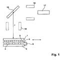
- Fig. 1 schematically shows the essential elements of an X-ray analyzer.
- the X-radiation emitted by a source 17 is modified by means of optical elements 18 and exposes an object 19 of special X-radiation.
- the X-ray beam is focused onto the detector by means of optical elements 18.
- the array detector is equipped with a X-ray sensitive single detector 1 , a first stage 2 of an evaluation (ASIC), a carrier 3 and a piezo drive 4 , wherein the single detector 1 by means of bumps 5 with the first stage.
- ASIC evaluation
- the transmitter to a further stage of the evaluation which may be located for example on the carrier 3 includes.
- a further stage of the evaluation which may be located for example on the carrier 3 includes.
- the mass of the components to be moved is kept low, so that the displacement can be done quickly and easily by using a piezoelectric drive 4, on the other hand, by the Mitverschieben the first stage 2 of the evaluation a low noise preamplification and first digital processing of the detected signals take place and thus a good signal / noise ratio can be achieved.
- the displacement of the single detector 1 takes place in one or in two dimensions such that the radial distance r of the single detector 1 to the object 19 does not change. The movement is indicated by the arrow. Thus, there is no need to focus on a new level.
- the single detector 1 off Fig. 1 is shown here in a flat design. However, it is also conceivable to provide curved embodiments.
- the X-ray sensitive pixel elements of the single detector 1 typically consist of Si or other semiconductor materials such as GaAs, CdTe, CZT.
- the transmitter 2 is typically implemented in CMOS or Bi-CMOS technology, eg in 0.35 ⁇ m feature sizes.
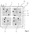
- a total detector 1 is in Fig. 2 shown. Since the individual sensor chips 8 , which are usually produced, are generally smaller than the desired single detector area, the single detector 1 is composed of a plurality of sensor chips 8. However, this has the consequence that, in addition to the defective pixel elements 9 contained in the sensor chips 8, edge regions 10 of the sensor chips 8 are additionally located within the individual detector area, from which information for the data record to be recorded can not be taken. Both the defective pixel elements 9 and the edge regions 10 of the sensor chips 8 therefore produce dead pixels 12 a, 12 b in a recorded data record 11 . In order to avoid distortions of information within a data set 11, defective pixel elements 9 in the data set are weighted with 0.
- blind pixel elements these also include pixel elements that generate strongly fluctuating signals or constantly reach their saturation value. Such pixel elements can be located by a 0-measurement.
- Common sensor chips include about 1,000 x 1,000 pixel elements. For simplicity, the in Fig. 2 shown sensor chips 8 shown with only 10 x 10 pixel elements.
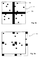
- Fig. 3a shows a schematic representation of the distribution of dead pixels 12a, 12b in a data record 11, which was recorded by a single detector 1, as shown in FIG Fig. 2 is shown.
- the isolated dead pixels 12a which result from the defective pixel elements 9 of the single detector 1
- this is impractical if the radiation to be detected has to be focused on a specific plane, as is required, for example, in Bragg-Brentano geometry in X-ray diffractometry.
- the sensor chips 8 are therefore arranged in a plane.
- the single detector 1 is moved after a first recording of a first data set in a position P1 from this position P1 to a position P2, as in Fig. 2 shown.
- a further data record 11 is recorded, which is superimposed with the first data record 11, so that a total data record 13 is formed.
- the width B of the blind edge regions of the sensor chips 8 in the method according to the invention is preferably an integer multiple of the width b of a pixel element, the width b of a pixel element moving in the order of 50 to 100 ⁇ m. In this way, it is possible to completely coincide a pixel element in position P1 with a pixel element in position P2 by shifting the single detector 1 by an integer multiple of a pixel element 7.
- Fig. 3b shows the distribution of the dead pixels 12 in the total data set 13, which is obtained from the data sets 11 of the measurements in the positions P1 and P2.
- the shift of the single detector 1 is chosen arbitrarily here and was 2x2 pixel elements. From the total data set 13, it can be seen that the number of dead pixels 12 compared with the number of dead pixels 12a, 12b in the data set 11 is Fig. 3 is considerably reduced. With a suitable optimization of the displacement of the individual detector 1, a further reduction of the dead pixels 12 in the overall data set 13 can be achieved, ideally dead pixels zero 12. Similarly, the result by recording more records 11 in different positions of the single detector 1 and their superposition an overall data record 13 can be improved.
- the predetermined measurement time can be selected long enough for the recordings of the individual data records 11 to be made.
- XRD X-Ray Diffraction
- each pixel element 7 can be assigned a statistical error as well as an offset for the recorded measured value, which are taken into account in the weighting of the respective pixel when the recorded data sets 11 are superimposed.
- the offset is subtracted for the data points to be superimposed, the measured value is normalized according to the sensitivity of the respective pixel element 7 and weighted inversely to the size of the associated statistical error, so that the overall weighting for each pixel is 1 or 100%.
- Fig. 4 this is shown schematically.
- a roughly structured rectangular single detector 8 is shifted diagonally to a position P2 (thin frame) around a sub-pixel element, in this case by half of a pixel element 7, after recording a first data set in a position P1 (bold frame). In this way, changes in the signal within a pixel can be detected, thereby increasing the spatial resolution of the entire data set.
- the advantages of the invention are particularly effective when one or more shifts are combined by an integer multiple of a pixel element 7 with one or more subsequent shifts by one subpixel. In this way, using a conventional single detector 1, one obtains a complete data set with a reduced number of dead pixels 12, ideally zero, and an improved spatial resolution.
- the application of the method according to the invention is not limited to rectangular sensor chips 8.
- radially symmetrical sensor chips 14 with ring segments as pixel elements, as in Fig. 5 can be used for this method.
- the displacement here takes place preferably in the form of a rotational movement about the midpoint of the radially symmetrical individual detector 14.
- it makes sense to use polar coordinates in such radially symmetrical sensor chips.
- the defective or weighted with 0 pixel elements 9 are moved to adjacent squares 16 , so that the dead pixels of the first record in the second record by fotosenisitver pixel elements 15 are measured and thus constructively contribute to the entire data set.
- the X-ray analysis device or the method according to the invention for operating an X-ray analysis device makes it possible in a simple manner, in particular without shifting the optical elements belonging to the X-ray analysis device, to reduce the dead pixels in the data record resulting from defective or 0-weighted pixel elements.
- a simple manner in particular without shifting the optical elements belonging to the X-ray analysis device, to reduce the dead pixels in the data record resulting from defective or 0-weighted pixel elements.
- interfering influences of the edge regions during the creation of data records can be avoided.
Landscapes
- Chemical & Material Sciences (AREA)
- Crystallography & Structural Chemistry (AREA)
- Physics & Mathematics (AREA)
- Health & Medical Sciences (AREA)
- Life Sciences & Earth Sciences (AREA)
- Analytical Chemistry (AREA)
- Biochemistry (AREA)
- General Health & Medical Sciences (AREA)
- General Physics & Mathematics (AREA)
- Immunology (AREA)
- Pathology (AREA)
- Analysing Materials By The Use Of Radiation (AREA)
- Measurement Of Radiation (AREA)
Claims (18)
- Procédé de fonctionnement d'un appareil d'analyse aux rayons X avec une source (17) de rayonnement X, un objet à examiner (19) qui est éclairé par le rayonnement X et un détecteur matriciel bidimensionnel plan pourvu d'éléments de pixels (7) pour la détection à résolution spatiale du rayonnement X provenant de l'objet (19), de sorte que l'on obtient un jeu de données, en particulier sous la forme d'un diffractogramme et/ou d'un spectre numérisé,
caractérisé par les étapes suivantes :(a) enregistrement d'un premier jeu de données (11) à une première position spatiale relative (P1) de la source (17), de l'objet (19) et du détecteur ;(b) déplacement et/ou rotation du détecteur dans la surface de détection par rapport à la source (17) et à l'objet (19), la position relative de la source (17) et de l'objet (19) n'étant pas modifiée ;(c) enregistrement d'un deuxième jeu de données (11) à la position (P2) déplacée selon l'étape (b), moins de 10 éléments de pixels (7) étant balayés par le déplacement et/ou la rotation du détecteur entre deux enregistrements de jeux de données (11) ;(d) superposition des jeux de données (11) enregistrés en un jeu de données total (13), les pixels des jeux de données enregistrés étant combinés en fonction de leur position relative effective par rapport à la source (17) et à l'objet (19). - Procédé selon la revendication 1, caractérisé en ce qu'avant l'étape (d), les étapes (b) à (c) sont répétées une fois ou plusieurs fois avec un déplacement variable.
- Procédé selon la revendication 2, caractérisé en ce que les jeux de données (11) sont enregistrés pendant un déplacement et/ou une rotation continus, de préférence périodiques du détecteur.
- Procédé selon la revendication 3, caractérisé en ce qu'entre deux enregistrements de jeux de données (11) successifs, le détecteur est déplacé d'exactement 1 élément de pixel (7).
- Procédé selon la revendication 3, caractérisé en ce qu'entre deux enregistrements de jeux de données (11) successifs, le détecteur est déplacé d'une fraction, de préférence de

- Procédé selon l'une des revendications 2 à 5, caractérisé en ce que les déplacements du détecteur comprennent des directions différentes dans la surface de détection.
- Procédé selon l'une des revendications précédentes, caractérisé en ce qu'à l'étape (d), les pixels des régions de bord du jeu de données total (13), auxquelles ne contribuent pas les jeux de données (11) de tous les enregistrements individuels, sont pondérés en fonction de l'inverse de leur fréquence d'enregistrement.
- Procédé selon l'une des revendications précédentes, caractérisé en ce qu'à chaque élément de pixel (7) sont associés individuellement une sensibilité et/ou une erreur statistique et/ou un décalage pour la valeur de mesure enregistrée, desquels il est tenu compte à l'étape (d) dans une pondération du pixel respectif lors de la superposition des jeux de données (11) enregistrés.
- Procédé selon la revendication 8, caractérisé en ce que la superposition des jeux de données (11) enregistrés est réalisée de manière que pour chacun des points de données à superposer, le décalage est soustrait, la valeur de mesure normalisée en fonction de la sensibilité de l'élément de pixel (7) respectif et pondérée inversement à la grandeur de l'erreur statistique associée, la pondération totale pour chaque pixel étant de 1, ou 100 %.
- Procédé selon la revendication 8 ou 9, caractérisé en ce que les contributions de certains éléments de pixels (9) lors de la superposition des jeux de données (11) à l'étape (d) sont pondérées de manière fixe par zéro, en particulier en cas d'éléments de pixels (9) défectueux, dont il est connu qu'ils sont aveugles, génèrent des signaux fortement fluctuants ou affichent en permanence leur valeur de saturation.
- Procédé selon la revendication 1, caractérisé en ce que les trajectoires du déplacement respectif sont adaptées à la répartition spatiale des éléments de pixels (9) défectueux, en particulier de manière que, dans la mesure du possible, aucun point de données du jeu de données total (13) ne soit constitué exclusivement de la superposition de contributions au signal d'éléments de pixels (9) défectueux.
- Procédé selon la revendication 10 ou 11, caractérisé en ce que le détecteur est composé de plusieurs puces de détection (8) adjacentes chaque fois par l'intermédiaire de régions de bord aveugles (10) et que les régions de bord aveugles (10) sont traitées comme des éléments de pixels (9) défectueux.
- Procédé selon l'une des revendications précédentes, caractérisé en ce que les trajectoires des déplacements respectifs sont choisies de manière à minimiser l'erreur statistique totale du jeu de données total (13).
- Appareil d'analyse aux rayons X conçu pour réaliser le procédé selon l'une des revendications 2 à 13, avec une source (17) de rayonnement X, un objet à examiner (19) qui est éclairé par le rayonnement X et un détecteur matriciel bidimensionnel plan pourvu d'éléments de pixels (7) pour la détection à résolution spatiale du rayonnement X provenant de l'objet (19), de sorte que l'on obtient un jeu de données, en particulier sous la forme d'un diffractogramme et/ou d'un spectre numérisé,
caractérisé en ce qu'il est prévu des moyens pour(a) enregistrer un premier jeu de données (11) à une première position spatiale relative (P1) de la source (17), de l'objet (19) et du détecteur,(b) déplacer et/ou tourner le détecteur dans la surface de détection par rapport à la source (17) et à l'objet (19), la position relative de la source (17) et de l'objet (19) n'étant pas modifiée ;(c) enregistrer un deuxième jeu de données (11) à la position (P2) déplacée selon l'étape (b),(d) superposer les jeux de données (11) enregistrés en un jeu de données total (13), les pixels des jeux de données (11) enregistrés étant combinés en fonction de leur position relative effective par rapport à la source (17) et à l'objet (19). - Appareil d'analyse aux rayons X selon la revendication 14, caractérisé en ce qu'il est prévu un entraînement piézoélectrique (4) pour déplacer le détecteur.
- Appareil d'analyse aux rayons X selon l'une des revendications 14 à 15, caractérisé en ce que le détecteur matriciel est disposé de manière mobile en commun avec un premier étage d'une électronique d'évaluation sur un support (3) qui n'est pas déplacé pendant la mesure, le premier étage étant relié électriquement par une liaison flexible (6) à un autre étage de l'électronique d'évaluation pour la transmission de signaux.
- Appareil d'analyse aux rayons X selon la revendication 16, caractérisé en ce que la liaison flexible (6) comprend une feuille mince, de préférence une feuille de polyimide, avec des pistes conductrices intégrées.
- Appareil d'analyse aux rayons X selon l'une des revendications 14 à 17 pour réaliser le procédé selon la revendication 13, caractérisé en ce que la largeur B des régions de bord aveugles (10) est un multiple entier de la largeur b d'un élément de pixel (7).
Applications Claiming Priority (2)
| Application Number | Priority Date | Filing Date | Title |
|---|---|---|---|
| DE102004025121A DE102004025121A1 (de) | 2004-05-21 | 2004-05-21 | Verfahren zum Betrieb eines Röntgenanalysegeräts mit zweidimensionalem Array-Detektor und Röntgenanalysegerät zum Durchführen des Verfahrens |
| DE102004025121 | 2004-05-21 |
Publications (3)
| Publication Number | Publication Date |
|---|---|
| EP1598663A2 EP1598663A2 (fr) | 2005-11-23 |
| EP1598663A3 EP1598663A3 (fr) | 2007-09-19 |
| EP1598663B1 true EP1598663B1 (fr) | 2008-12-24 |
Family
ID=34936239
Family Applications (1)
| Application Number | Title | Priority Date | Filing Date |
|---|---|---|---|
| EP05009958A Expired - Lifetime EP1598663B1 (fr) | 2004-05-21 | 2005-05-06 | Procédé et appareil d'analyse aux rayons X avec un Réseau de détecteurs bidemensionnel |
Country Status (3)
| Country | Link |
|---|---|
| US (1) | US7136454B2 (fr) |
| EP (1) | EP1598663B1 (fr) |
| DE (2) | DE102004025121A1 (fr) |
Cited By (1)
| Publication number | Priority date | Publication date | Assignee | Title |
|---|---|---|---|---|
| CN105593670A (zh) * | 2013-11-26 | 2016-05-18 | 株式会社理学 | X射线衍射装置和x射线衍射测定方法 |
Families Citing this family (26)
| Publication number | Priority date | Publication date | Assignee | Title |
|---|---|---|---|---|
| EP1978875B1 (fr) * | 2006-01-16 | 2019-07-10 | Koninklijke Philips N.V. | Module intelligent de détecteurs de rayonnement |
| US7920676B2 (en) * | 2007-05-04 | 2011-04-05 | Xradia, Inc. | CD-GISAXS system and method |
| DE102007042144A1 (de) * | 2007-09-05 | 2009-03-12 | Smiths Heimann Gmbh | Verfahren zur Verbesserung der Materialerkennbarkeit in einer Röntgenprüfanlage und Röntgenprüfanlage |
| KR100923097B1 (ko) * | 2008-01-15 | 2009-10-22 | (주)이우테크놀로지 | X선 촬영장치 |
| US8265369B2 (en) * | 2009-04-16 | 2012-09-11 | Apteryx, Inc. | Apparatus and method for virtual flaw removal from X-ray sensitive plates |
| US20100303208A1 (en) * | 2009-05-29 | 2010-12-02 | Oliver Baruth | Method for recording an x-ray image, x-ray detector and x-ray system |
| JP5534756B2 (ja) * | 2009-09-16 | 2014-07-02 | キヤノン株式会社 | 画像処理装置、画像処理方法、画像処理システム及びプログラム |
| RU2423026C1 (ru) * | 2010-03-09 | 2011-06-27 | Общество с ограниченной ответственностью "Научно-производственное предприятие ВЭЛИТ" | Устройство для облучения объектов рентгеновскими лучами |
| EP2675358B1 (fr) * | 2011-02-17 | 2016-11-09 | Analogic Corporation | Mosaïque de détecteurs possédant une dimension utile supérieure à la dimension réelle |
| US10247682B2 (en) | 2013-04-04 | 2019-04-02 | Illinois Tool Works Inc. | Helical computed tomography |
| JP6105806B2 (ja) | 2013-04-12 | 2017-03-29 | イリノイ トゥール ワークス インコーポレイティド | 高解像度コンピュータートモグラフィー |
| US9022651B2 (en) * | 2013-07-12 | 2015-05-05 | Bruker Axs, Inc. | X-ray diffraction-based defective pixel correction method using an active pixel array sensor |
| JP6242185B2 (ja) | 2013-11-22 | 2017-12-06 | 株式会社リガク | 補正情報生成方法および補正情報生成装置 |
| JP6135526B2 (ja) | 2014-01-30 | 2017-05-31 | 株式会社リガク | 画像処理方法および画像処理装置 |
| JP6524473B2 (ja) | 2014-10-24 | 2019-06-05 | 株式会社リガク | データ処理装置、各ピクセルの特性を求める方法ならびにデータ処理の方法およびプログラム |
| DE102015213911B4 (de) * | 2015-07-23 | 2019-03-07 | Siemens Healthcare Gmbh | Verfahren zum Erzeugen eines Röntgenbildes und Datenverarbeitungseinrichtung zum Ausführen des Verfahrens |
| DE102017205096B3 (de) * | 2017-03-27 | 2018-08-02 | Siemens Healthcare Gmbh | Akquisition von Bildern mit einem Strahlungsdetektor |
| EP3569148B1 (fr) * | 2018-05-17 | 2023-01-11 | Siemens Healthcare GmbH | Procédé d'enregistrement d'un ensemble de données d'image au moyen d'un détecteur de rayons x |
| US12281993B2 (en) | 2021-09-15 | 2025-04-22 | Illinois Tool Works Inc. | High resolution continuous rotation industrial radiography imaging processes |
| US20230316467A1 (en) * | 2022-04-05 | 2023-10-05 | Baker Hughes Holdings Llc | Digital Detector Array Correction |
| CN116893185A (zh) * | 2022-04-05 | 2023-10-17 | 贝克休斯控股有限责任公司 | 数字检测器阵列校正 |
| US12332192B2 (en) | 2022-04-20 | 2025-06-17 | Arion Diagnostics, Inc. | Alpha diffractometer |
| US12336851B2 (en) * | 2022-04-20 | 2025-06-24 | Arion Diagnostics, Inc. | Diffractive analyzer of patient tissue |
| DE102022209048A1 (de) * | 2022-08-31 | 2024-02-29 | Carl Zeiss Microscopy Gmbh | Überlappendes Pixelbinning in Kamerabildern |
| US12607578B2 (en) | 2023-06-15 | 2026-04-21 | Illinois Tool Works Inc. | Accelerated higher resolution industrial radiography |
| DE102024200530A1 (de) | 2024-01-22 | 2025-02-27 | Siemens Healthineers Ag | Röntgendetektorvorrichtung, Mehrlagenflächendetektor und Verfahren |
Family Cites Families (10)
| Publication number | Priority date | Publication date | Assignee | Title |
|---|---|---|---|---|
| US5491738A (en) * | 1993-03-15 | 1996-02-13 | The United States Of America As Represented By The Administrator Of The National Aeronautics And Space Administration | X-ray diffraction apparatus |
| US5847398A (en) | 1997-07-17 | 1998-12-08 | Imarad Imaging Systems Ltd. | Gamma-ray imaging with sub-pixel resolution |
| US6064717A (en) * | 1997-11-21 | 2000-05-16 | Rigaku/Usa, Inc. | Unrestricted motion apparatus and method for x-ray diffraction analysis |
| DE19800946A1 (de) * | 1998-01-13 | 1999-07-22 | Siemens Ag | Volumen-Computertomographiesystem |
| US6118846A (en) * | 1999-02-23 | 2000-09-12 | Direct Radiography Corp. | Bad pixel column processing in a radiation detection panel |
| DE10043474B4 (de) * | 2000-09-04 | 2007-08-09 | Siemens Ag | Detektor zum Erzeugen eines Bildes aus einfallender Strahlung |
| DE10047366A1 (de) * | 2000-09-25 | 2002-05-08 | Siemens Ag | Strahlungsdetektor |
| US6408047B1 (en) * | 2000-10-04 | 2002-06-18 | Rigaku/Msc, Inc. | Method of providing high throughput protein crystallography |
| DE10244181A1 (de) | 2002-09-23 | 2004-04-01 | Siemens Ag | Verfahren zur Bilderstellung in der Computertomographie und CT-Gerät zur Durchführung des Verfahrens |
| DE10307752B4 (de) * | 2003-02-14 | 2007-10-11 | Siemens Ag | Röntgendetektor |
-
2004
- 2004-05-21 DE DE102004025121A patent/DE102004025121A1/de not_active Ceased
-
2005
- 2005-04-21 US US11/110,900 patent/US7136454B2/en not_active Expired - Lifetime
- 2005-05-06 EP EP05009958A patent/EP1598663B1/fr not_active Expired - Lifetime
- 2005-05-06 DE DE502005006309T patent/DE502005006309D1/de not_active Expired - Lifetime
Cited By (2)
| Publication number | Priority date | Publication date | Assignee | Title |
|---|---|---|---|---|
| CN105593670A (zh) * | 2013-11-26 | 2016-05-18 | 株式会社理学 | X射线衍射装置和x射线衍射测定方法 |
| CN105593670B (zh) * | 2013-11-26 | 2019-06-04 | 株式会社理学 | X射线衍射装置和x射线衍射测定方法 |
Also Published As
| Publication number | Publication date |
|---|---|
| DE502005006309D1 (de) | 2009-02-05 |
| US7136454B2 (en) | 2006-11-14 |
| EP1598663A2 (fr) | 2005-11-23 |
| DE102004025121A1 (de) | 2005-12-15 |
| EP1598663A3 (fr) | 2007-09-19 |
| US20050259790A1 (en) | 2005-11-24 |
Similar Documents
| Publication | Publication Date | Title |
|---|---|---|
| EP1598663B1 (fr) | Procédé et appareil d'analyse aux rayons X avec un Réseau de détecteurs bidemensionnel | |
| DE19604802C2 (de) | Abbildungssystem und Verfahren zum Erzeugen einer Querschnittsabbildung eines Objekts | |
| DE69410685T2 (de) | Hochauflösendes Strahlungsabbildungssystem | |
| DE60204764T2 (de) | Verfahren und vorrichtung zur messung der position, form, grösse und intensitätsverteilung eines effektiven röntgenröhrenfokus | |
| DE602004012080T2 (de) | Nachweis von ionisierender strahlung auf dual-energie-scanning-basis | |
| EP0357944B1 (fr) | Installation de radiodiagnostic dentaire pour réaliser une tomographie panoramique de la mâchoire d'un patient | |
| DE3786091T2 (de) | Herstellung tomographischer abbildungen. | |
| DE102011053971A1 (de) | Verfahren und Vorrichtung zum Erfassen der Struktur von bewegten Stückgütern, insbesondere zur Erfassung von Störpartikeln in flüssigen oder pastösen Produkten | |
| DE10244176A1 (de) | Bilddetektor für Röntgenstrahlung | |
| DE102014117251A1 (de) | Röntgentopographievorrichtung | |
| DE10322712A1 (de) | Strahlungsquellenpositions-Erfassungsverfahren, Strahlungsquellenpositions-Erfassungssystem, und Strahlungsquellenpositions-Erfassungssonde | |
| DE69714105T2 (de) | Vorrichtung zur Transversabschichtbildern | |
| DE19526930A1 (de) | Detektorsignal-Integration von volumetrischen CT Scanner-Detektorarrays | |
| DE102019121829B4 (de) | Strahlungsdetektoranordnung mit anoden zur verbesserten erkennung von nicht gesammelten benachbarten signalen | |
| CH616581A5 (fr) | ||
| EP3569148A1 (fr) | Procédé d'enregistrement d'un ensemble de données d'image au moyen d'un détecteur de rayons x | |
| DE4310622A1 (de) | Einrichtung zur Mikrobilderzeugung mittels ionisierender Strahlung | |
| DE3410885A1 (de) | Fehlerkorrigierte korpuskularstrahllithographie | |
| EP1347287B1 (fr) | Diffusion cohérente de rayons X avec multifocalisation simultanée (CXRS) | |
| EP0065803B1 (fr) | Dispositif d'examen de rayons X | |
| DE102004028392A1 (de) | Centroid-Einrichtung und -Verfahren zur Sub-Pixelauflösung von Röntgenbildern | |
| DE2640832B2 (de) | Elektroakustische vorrichtung zum lesen eines eindimensionalen optischen bildes | |
| EP1672358B1 (fr) | Dispositif pour mesurer le spectre de transfert d'impulsions de quanta de rayons X diffractés élastiquement ainsi qu'une méthode pour déterminer ce spectre de transfert d'impulsions | |
| DE10164245A1 (de) | Verfahren zum Kompensieren eines Spaltes bei volumetrischen Mehrfachplatten-CT-Abtastern und zugehörige Vorrichtung | |
| EP3928085B1 (fr) | Dispositif de mesure de rayonnement x pour une mesure 1d continue |
Legal Events
| Date | Code | Title | Description |
|---|---|---|---|
| PUAI | Public reference made under article 153(3) epc to a published international application that has entered the european phase |
Free format text: ORIGINAL CODE: 0009012 |
|
| AK | Designated contracting states |
Kind code of ref document: A2 Designated state(s): AT BE BG CH CY CZ DE DK EE ES FI FR GB GR HU IE IS IT LI LT LU MC NL PL PT RO SE SI SK TR |
|
| AX | Request for extension of the european patent |
Extension state: AL BA HR LV MK YU |
|
| PUAL | Search report despatched |
Free format text: ORIGINAL CODE: 0009013 |
|
| AK | Designated contracting states |
Kind code of ref document: A3 Designated state(s): AT BE BG CH CY CZ DE DK EE ES FI FR GB GR HU IE IS IT LI LT LU MC NL PL PT RO SE SI SK TR |
|
| AX | Request for extension of the european patent |
Extension state: AL BA HR LV MK YU |
|
| 17P | Request for examination filed |
Effective date: 20071018 |
|
| 17Q | First examination report despatched |
Effective date: 20080110 |
|
| AKX | Designation fees paid |
Designated state(s): DE GB NL |
|
| GRAP | Despatch of communication of intention to grant a patent |
Free format text: ORIGINAL CODE: EPIDOSNIGR1 |
|
| GRAS | Grant fee paid |
Free format text: ORIGINAL CODE: EPIDOSNIGR3 |
|
| GRAA | (expected) grant |
Free format text: ORIGINAL CODE: 0009210 |
|
| AK | Designated contracting states |
Kind code of ref document: B1 Designated state(s): DE GB NL |
|
| REG | Reference to a national code |
Ref country code: GB Ref legal event code: FG4D Free format text: NOT ENGLISH |
|
| REF | Corresponds to: |
Ref document number: 502005006309 Country of ref document: DE Date of ref document: 20090205 Kind code of ref document: P |
|
| PLBE | No opposition filed within time limit |
Free format text: ORIGINAL CODE: 0009261 |
|
| STAA | Information on the status of an ep patent application or granted ep patent |
Free format text: STATUS: NO OPPOSITION FILED WITHIN TIME LIMIT |
|
| 26N | No opposition filed |
Effective date: 20090925 |
|
| PGFP | Annual fee paid to national office [announced via postgrant information from national office to epo] |
Ref country code: GB Payment date: 20210525 Year of fee payment: 17 |
|
| GBPC | Gb: european patent ceased through non-payment of renewal fee |
Effective date: 20220506 |
|
| PG25 | Lapsed in a contracting state [announced via postgrant information from national office to epo] |
Ref country code: GB Free format text: LAPSE BECAUSE OF NON-PAYMENT OF DUE FEES Effective date: 20220506 |
|
| P01 | Opt-out of the competence of the unified patent court (upc) registered |
Effective date: 20231116 |
|
| PGFP | Annual fee paid to national office [announced via postgrant information from national office to epo] |
Ref country code: NL Payment date: 20240522 Year of fee payment: 20 |
|
| PGFP | Annual fee paid to national office [announced via postgrant information from national office to epo] |
Ref country code: DE Payment date: 20240517 Year of fee payment: 20 |
|
| REG | Reference to a national code |
Ref country code: DE Ref legal event code: R071 Ref document number: 502005006309 Country of ref document: DE |
|
| REG | Reference to a national code |
Ref country code: NL Ref legal event code: MK Effective date: 20250505 |