EP1601032B1 - Impression par jet d'encre d'un panneau d'affichage organique électroluminescent - Google Patents
Impression par jet d'encre d'un panneau d'affichage organique électroluminescent Download PDFInfo
- Publication number
- EP1601032B1 EP1601032B1 EP05007001A EP05007001A EP1601032B1 EP 1601032 B1 EP1601032 B1 EP 1601032B1 EP 05007001 A EP05007001 A EP 05007001A EP 05007001 A EP05007001 A EP 05007001A EP 1601032 B1 EP1601032 B1 EP 1601032B1
- Authority
- EP
- European Patent Office
- Prior art keywords
- layer
- light emitting
- partition wall
- wall portion
- electro
- Prior art date
- Legal status (The legal status is an assumption and is not a legal conclusion. Google has not performed a legal analysis and makes no representation as to the accuracy of the status listed.)
- Expired - Fee Related
Links
Images







Classifications
-
- H—ELECTRICITY
- H10—SEMICONDUCTOR DEVICES; ELECTRIC SOLID-STATE DEVICES NOT OTHERWISE PROVIDED FOR
- H10K—ORGANIC ELECTRIC SOLID-STATE DEVICES
- H10K71/00—Manufacture or treatment specially adapted for the organic devices covered by this subclass
- H10K71/10—Deposition of organic active material
- H10K71/12—Deposition of organic active material using liquid deposition, e.g. spin coating
- H10K71/13—Deposition of organic active material using liquid deposition, e.g. spin coating using printing techniques, e.g. ink-jet printing or screen printing
- H10K71/135—Deposition of organic active material using liquid deposition, e.g. spin coating using printing techniques, e.g. ink-jet printing or screen printing using ink-jet printing
-
- H—ELECTRICITY
- H05—ELECTRIC TECHNIQUES NOT OTHERWISE PROVIDED FOR
- H05B—ELECTRIC HEATING; ELECTRIC LIGHT SOURCES NOT OTHERWISE PROVIDED FOR; CIRCUIT ARRANGEMENTS FOR ELECTRIC LIGHT SOURCES, IN GENERAL
- H05B33/00—Electroluminescent light sources
- H05B33/10—Apparatus or processes specially adapted to the manufacture of electroluminescent light sources
-
- H—ELECTRICITY
- H05—ELECTRIC TECHNIQUES NOT OTHERWISE PROVIDED FOR
- H05B—ELECTRIC HEATING; ELECTRIC LIGHT SOURCES NOT OTHERWISE PROVIDED FOR; CIRCUIT ARRANGEMENTS FOR ELECTRIC LIGHT SOURCES, IN GENERAL
- H05B33/00—Electroluminescent light sources
- H05B33/12—Light sources with substantially two-dimensional [2D] radiating surfaces
- H05B33/22—Light sources with substantially two-dimensional [2D] radiating surfaces characterised by the chemical or physical composition or the arrangement of auxiliary dielectric or reflective layers
-
- H—ELECTRICITY
- H10—SEMICONDUCTOR DEVICES; ELECTRIC SOLID-STATE DEVICES NOT OTHERWISE PROVIDED FOR
- H10K—ORGANIC ELECTRIC SOLID-STATE DEVICES
- H10K71/00—Manufacture or treatment specially adapted for the organic devices covered by this subclass
- H10K71/40—Thermal treatment, e.g. annealing in the presence of a solvent vapour
-
- H—ELECTRICITY
- H10—SEMICONDUCTOR DEVICES; ELECTRIC SOLID-STATE DEVICES NOT OTHERWISE PROVIDED FOR
- H10K—ORGANIC ELECTRIC SOLID-STATE DEVICES
- H10K59/00—Integrated devices, or assemblies of multiple devices, comprising at least one organic light-emitting element covered by group H10K50/00
- H10K59/10—OLED displays
- H10K59/12—Active-matrix OLED [AMOLED] displays
- H10K59/122—Pixel-defining structures or layers, e.g. banks
-
- H—ELECTRICITY
- H10—SEMICONDUCTOR DEVICES; ELECTRIC SOLID-STATE DEVICES NOT OTHERWISE PROVIDED FOR
- H10K—ORGANIC ELECTRIC SOLID-STATE DEVICES
- H10K59/00—Integrated devices, or assemblies of multiple devices, comprising at least one organic light-emitting element covered by group H10K50/00
- H10K59/30—Devices specially adapted for multicolour light emission
- H10K59/35—Devices specially adapted for multicolour light emission comprising red-green-blue [RGB] subpixels
-
- H—ELECTRICITY
- H10—SEMICONDUCTOR DEVICES; ELECTRIC SOLID-STATE DEVICES NOT OTHERWISE PROVIDED FOR
- H10K—ORGANIC ELECTRIC SOLID-STATE DEVICES
- H10K59/00—Integrated devices, or assemblies of multiple devices, comprising at least one organic light-emitting element covered by group H10K50/00
- H10K59/30—Devices specially adapted for multicolour light emission
- H10K59/38—Devices specially adapted for multicolour light emission comprising colour filters or colour changing media [CCM]
-
- H—ELECTRICITY
- H10—SEMICONDUCTOR DEVICES; ELECTRIC SOLID-STATE DEVICES NOT OTHERWISE PROVIDED FOR
- H10K—ORGANIC ELECTRIC SOLID-STATE DEVICES
- H10K71/00—Manufacture or treatment specially adapted for the organic devices covered by this subclass
Definitions
- the present invention relates to a method of manufacturing an electro-optical device.
- a substrate on which pixel electrodes and banks for partitioning the pixel electrodes are formed is prepared, and hole injection/transport layers are formed in a region surrounded by the banks using the inkjet method.
- ink for a red color light emitting layer filled in an inkjet head, is dropped in the region surrounded by the banks, and thereafter, the dropped ink is dried to form the red color emitting layer.
- ink for a green color light emitting layer is disposed on fixed points on the substrate using the inkjet head, to thereby form a green color light emitting layer through the drying process.
- ink for a blue color light emitting layer is disposed on fixed points on the substrate using the inkjet head, to thereby form a blue color light emitting layer through the drying process.
- the color organic EL device is manufactured by disposing the red, green and blue color light emitting layers on the substrate in a predetermined pattern.
- the light emitting layers having the different light emitting colors are formed, a manufacturing method for dropping and drying one color ink, and then, forming light emitting layers having different colors is in common use. This is because the light emitting layers having the different colors have different ink solvent due to differences of ink components, and accordingly, optimal drop and dry conditions are different for each color.
- the present invention is designed to solve the above-mentioned problem, and it is an object of the present invention to provide a manufacturing method of a color filter substrate having a plurality of coloring layers, which is capable of greatly improving a manufacture efficiency of the color filter substrate and improving film thickness uniformity and flatness of each coloring layer to be formed. It is another object of the present invention to provide a manufacturing method of an electro-optical device having a plurality of electro-optical layers such as a plurality of light emitting layers, which is capable of greatly improving a manufacture efficiency of the electro-optical device and improving film thickness uniformity and flatness of each electro-optical layer to be formed.
- the present invention provides a method of manufacturing an electro-optical device including different types of electro-optical layers in a predetermined pattern, the method comprising a partition wall portion formation step of forming on a substrate a first partition wall portion having a first opening defining a region in which the electro-optical layers are formed and a second partition wall portion located on the first partition wall portion and having a second opening defining a region in which the electro-optical layers are formed; and an ejection step of ejecting liquid substances for the openings of the partition wall portions by using a liquid droplet ejecting method, the liquid substances being made by dissolving or dispersing functional materials composing the respective electro-optical layers in solvents, wherein the ejected liquid substances have higher and lower viscosities for each electro-optical layer, and wherein, in the partition wall portion formation step, the first partition wall portion projects from an inner surface of the second opening of the second partition wall portion, a surface area of a portion of the
- the present inventors have repeated studies for overcoming the above-mentioned problem, and as a result, have discovered that the film thickness of the formed electro-optical layers becomes ununiform due to the viscosity of the liquid substance, that is, when the viscosity of the liquid substance is high, the film thickness of the electro-optical layer formed in the opening of the partition wall portion tends to become thick at a central portion of the electro-optical layer, on the other hand, when the viscosity of the liquid substance is low, the film thickness of the electro-optical layer formed in the opening of the partition wall portion tends to become thick at a peripheral portion (a side near the partition wall portion) of the electro-optical layer.
- the present inventors have discovered that the film thickness of the formed electro-optical layers becomes ununiform due to the surface area of a portion (projecting portion) of the first partition wall portion projecting from an inner surface of the second opening of the second partition wall portion, that is, when the surface area of the projecting portion of the first partition wall portion is small, the film thickness of the electro-optical layer formed in the opening of the partition wall portion tends to become thick at a central portion of the electro-optical layer, on the other hand, when the surface area of the projecting portion of the first partition wall portion is large, the film thickness of the electro-optical layer formed in the opening of the partition wall portion tends to become thick at a peripheral portion (a side near the partition wall portion) of the electro-optical layer.
- the present inventors have discovered a method of forming flat electro-optical layers having a uniform film thickness even when the viscosities of the liquid substances are different for each pattern of the electro-optical layers.
- the film thickness of the electro-optical layers can become uniform and the electro-optical layers can become flat by properly adjusting the area of the projecting portion of the first partition wall portion according to the viscosity of the liquid substances, as in the manufacturing method of the present invention, more specifically, by making a surface area of the projecting portion of the first partition wall portion relatively small in an opening through which the liquid substance having relatively low viscosity is ejected, and making the surface area of the projecting portion of the first partition wall portion relatively large in an opening through which the liquid substance having relatively high viscosity is ejected.
- the projecting length of the first partition wall portion projecting from the inner surface of the second opening of the second partition wall portion can become smaller in an opening through which the liquid substance having a lower viscosity is ejected than the projecting length of the first partition wall portion projecting from the second partition wall portion in an opening through which the liquid substance having higher viscosity is ejected.
- the surface area of the projecting portion can be easily adjusted.
- the method of manufacturing an electro-optical device further comprises, after the ejection step, a drying step of drying the ejected liquid substances simultaneously for electro-optical layers.
- a drying step of drying the ejected liquid substances simultaneously for electro-optical layers In this way, by drying the electro-optical layers collectively, the product efficiency of the electro-optical devices can be greatly enhanced over the conventional product efficiency of the electro-optical devices.
- the drying step is a vacuum drying step.
- a vacuum dry in order to dry the liquid substance coated on the substrate, it is possible to control dry conditions minutely. Accordingly, after the drying step, the electro-optical layers having a uniform film thickness and a good flatness can be obtained.
- the present invention may be applied to an electro-optical device itself not part of the invention but manufactured by the manufacturing method of the present invention.
- an electronic apparatus itself not part of the invention may comprise the electro-optical device as, for example, a display unit. Accordingly, electro-optical devices and electronic apparatuses can be manufactured at low costs and with high reliability.
- FIG. 1 is an explanatory diagram illustrating an interconnection structure of an organic EL device
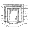
- Fig. 2 is a schematic plan view of the organic EL device
- Fig. 3 is a schematic sectional view of a display region of the organic EL device.
- an organic EL device includes a plurality of scan lines 101, a plurality of data lines 102 extending cross the plurality of scan lines 101, a plurality of power lines extending in parallel to the plurality of data lines 102, and pixel regions P provided in the vicinity of intersections of the plurality of scan lines 101 and the plurality of data lines 102.
- a scan line driving circuit 105 having a shift register and a level shifter is connected to the scan lines 101.
- each of the pixel circuits P includes a switching thin film transistor 122 having a gate electrode to which a scan signal is applied via a scan line 101, a storage capacitor cap for storing a pixel signal supplied from the data line 102 via the switching thin film transistor 122, a driving thin film transistor 123 of which a gate electrode receives the pixel signal stored in the storage capacitor cap, a pixel electrode (electrode) 111 into which a driving current flows from a corresponding power line 103 when the pixel electrode 111 is electrically connected to the power line 103 via the driving thin film transistor 123, and an organic EL layer 110 inserted between the pixel electrode 111 and a negative electrode (opposite electrode) 12.
- the pixel electrode 111, the opposite electrode 12 and the organic EL layer 110 compose a light emitting element.
- a potential of the data line 102 is maintained by the storage capacitor cap and the driving thin film transistor 123 is turned on or off depending on the state of the storage capacitor cap.
- a current flows from the power line 103 into the pixel electrode 111 via a channel of the driving thin film transistor 123 and a current flows into the negative electrode 12 via the organic EL layer 110.
- the organic EL layer 110 emits light in proportion to the amount of the current flowing into the organic EL layer 110.
- the organic EL device includes a transparent substrate 2 made of glass and the like, a light emitting element portion 11 having light emitting elements formed on the substrate 2 and arranged in the form of a matrix, and the negative electrode 12 formed on the light emitting element portion 11.
- the light emitting element portion 11 and the negative electrode 12 compose a display element 10.
- the substrate 2 is formed of a transparent substrate such as glass and the like, and is divided into a display region 2a located at the center of the substrate 2 and a non-display region 2c located at the circumference of the substrate 2 and surrounding the display region 2a, as shown in Fig. 2 .
- the display region 2a is a region in which the light emitting elements arranged in the form of the matrix are formed.
- the power lines 103 (103R, 103G, and 103B) are arranged in the non-display region 2c.
- the scan line driving circuits 105 and 105 are arranged in both sides of the display region 2a, respectively.
- a driving circuit control signal line 105a and a driving circuit power line 105b are arranged at one side of each of the scan line driving circuits 105 and 105, both of which are connected to each line driving circuit 105 and 105.
- a check circuit 106 for checking quality or defects of a display device when it is in the course of manufacturing or in the market is arranged above the display region 2a.
- a circuit element portion 14 having circuits such as thin film transistors (TFTs), the light emitting element portion 11 having the organic EL layer 110, and the negative electrode 12 are stacked in order on the substrate 2.
- TFTs thin film transistors
- the light emitting element portion 11 having the organic EL layer 110, and the negative electrode 12 are stacked in order on the substrate 2.
- light emitted from the organic EL layer 110 to the substrate 2 is outputted to a lower side (observer side) of the substrate 2 through the circuit element portion 14 and the substrate 2, and simultaneously, light emitted from the organic EL layer 110 to the opposite side of the substrate 2 is reflected by the negative electrode 12 and then is outputted to the lower side (observer side) of the substrate 2 through the circuit element portion 14 and the substrate 2.
- the negative electrode 12 when the negative electrode 12 is formed of a transparent material, light emitted from the negative electrode side can be outputted to the lower side of the substrate 2.
- the transparent negative electrode material may include an indium tin oxide (ITO), Pt, Ir, Ni, or Pd.
- a base protective layer 2c made of a silicon oxide is formed in the circuit element portion 14 on the substrate 2, and an island-shaped semiconductor layer 141 made of polycrystalline silicon is formed on the base protective layer 2c.
- a source region 141a and a drain region 141b are formed in the semiconductor layer 141 by heavily doping P ions into the semiconductor layer 141.
- a portion of the semiconductor layer 141 into which the P ions are not doped forms a channel region 141c.
- a transparent gate insulating layer 142 covering the base protective layer 2c and the semiconductor layer 141 is formed, a gate electrode 143 (scan line 101) made of Al, Mo, Ta, Ti, or W is formed on the gate insulating layer 142, and a first transparent interlayer insulating layer 144a and a second transparent interlayer insulating layer 144b are formed on the gate electrode 143 and the gate insulating layer 142.
- the gate electrode 143 is disposed at a location corresponding to the channel region 141c of the semiconductor layer 141.
- contact holes 145 and 146 are connected to the source and drain regions 141a and 141b of the semiconductor layers 141 through the first and second interlayer insulating layers 144a and 144b, respectively.
- the transparent pixel electrode 111 made of ITO and the like is formed with a predetermined pattern on the second interlayer insulating layer 144b, and the contact hole 145 is connected to the pixel electrode 111.
- the contact hole 146 is connected to the power line 103. In this way, the driving thin film transistor 123 connected to the pixel electrode 111 is formed in the circuit element portion 14.
- the light emitting element portion 11 includes, as a main body, organic EL layers 110 stacked on each of the plurality of pixel electrodes 111 , and bank portions 112 formed between pixel electrodes 111 and between organic EL layers 110 for partitioning the organic EL elements 110.
- the negative electrode 12 is formed on the organic EL layers 110.
- the pixel electrodes 111, the organic EL layers 110 and the negative electrode 12 compose the light emitting element.
- each pixel electrode 111 is made of, for example, ITO, and has a substantially rectangular pattern in a plane.
- the bank portions 112 have shapes of partitioning the pixel electrodes 111.
- each of the bank portions 112 has a structure where an inorganic bank layer (first bank layer) 112a, which serves as a first partition wall portion, located at the substrate 2 side and an organic bank layer (second bank layer) 112b, which serves as a second partition wall portion, spaced apart from the substrate 2 are stacked.
- the inorganic bank layer 112a is formed of, for example, TiO 2 or SiO 2
- the organic bank layer 112b is formed of, for example, an acryl resin or a polyimide resin.
- the inorganic and organic bank layers 112a and 112b are formed in such a manner that they are placed on the peripheral portions of the pixel electrodes 111. When viewed from a plane, the peripheral portions of the pixel electrodes 111 partially overlap with the inorganic bank layer 112a. Similarly, the organic bank layer 112b overlaps with portions of the pixel electrodes 111 when viewed from the plane. In addition, the inorganic bank layer 112a is formed to further project toward the centers of the pixel electrodes 111 beyond an edge of the organic bank layer 112b. In this way, as a first stack portion (projecting portion) 112e of the inorganic bank layer 112a is formed inside the pixel electrodes 111, lower openings 112c corresponding to formation locations of the pixel electrodes 111 are formed.
- upper openings 112d are formed in the organic bank layer 112b.
- the upper openings 112d are provided corresponding to the formation locations of the pixel electrodes 111 and the lower openings 112c.
- the upper openings 112d are formed to be wider than the lower openings 112c and narrower than the pixel electrodes 111, as shown in Fig. 3 .
- upper portions of the upper openings 112d may be formed at the about same positions as end portions of the pixel electrodes 111. In this case, as shown in Fig. 3 , the upper openings 112d of the organic bank layer 112b have inclined sections. In this way, openings 112g through which the lower openings 112c communicate with the upper openings 112d are formed in the bank portion 112.
- the bank portion 112 has lyophilic regions and lyophobic regions.
- the lyophilic regions include the first stack portion 112e of the inorganic bank layer 112a and an electrode surface 111a of each pixel electrode 111. Surfaces of these regions are processed by lyophilic substance using a plasma process using oxygen as a process gas.
- the lyophobic regions include a wall of each upper opening 112d and a top surface 112f of the organic bank layer 112. Surfaces of these regions are processed by fluorine (by lyophobic substance) using a plasma process using tetrafluoromethane or carbon tetrafluoride as a process gas.
- the organic EL layer 110 includes a hole injection/transport layer 110a stacked on the pixel electrode 111 and a light emitting layer 110b formed on the hole injection/transport layer 110a.
- the hole injection/transport layer 110a serves to inject holes into the light emitting layer 110b and transport holes into the hole injection/transport layer 110a.
- characteristics such as light emission efficiency and lifetime of the light emission layer 110b can be improved.
- the light emission layer 110b emits light as holes injected from the hole injection/transport layer 110a and electrons injected from the negative electrode 12 are recombined in the light emitting layer 110b.
- the hole injection/transport layer 110a includes a flat portion 110a1 located within the lower opening 112c and formed on the pixel electrode surface 111a, and a peripheral portion 110a2 located within the upper opening 112d and formed on the first stack portion 112e of the inorganic bank layer.
- the hole injection/transport layer 110a may be formed on the pixel electrode 111 and only between the inorganic bank layers 112a (at the lower openings 112c) depending on its structure (or may be formed only on the above mentioned flat portion).
- the light emitting layer 110b is formed on the flat portion 110a1 and peripheral portion 110a2 of the hole injection/transport layer 110a and has a thickness of 50 nm to 80 nm on the flat portion 110a1.
- the light emitting layer 110b has three kinds of light emitting layers, i.e., a red color light emitting layer 110b1 emitting red color (R) light, a green color light emitting layer 110b2 emitting green color (G) light, and a blue color light emitting layer 110b3 emitting blue color (B) light, which are arranged in a stripe shape, as shown in Fig. 2 .
- the peripheral portion 110a2 is formed at a ununiform thickness on the first stack portion 112e of the inorganic bank layer, it is electrically isolated from the pixel electrode 111 by the first stack portion 112e, and accordingly, holes are not injected from the peripheral portion 110a2 into the light emitting layer 110b. Accordingly, a current from the pixel electrode 111 flows only into the flat portion 110a1, and accordingly, the holes can be uniformly transported from the flat portion 110a1 to the light emitting layer 110b. As a result, only a central portion of the light emitting layer 110b emits light and the amount of light emission in the light emitting layer 110b can be uniformly maintained.
- the inorganic bank layer 112a extends toward the center of the pixel electrode 111 more than the organic bank layer 112b, a shape of a junction portion between the pixel electrode 111 and the flat portion 110a1 is trimmed by the inorganic bank layer 112a. Accordingly, deviation of light emission strength between the light emitting layers 110b can be suppressed.
- the organic EL layer 110 is uniformly stuck fast to the pixel electrode 111 and the inorganic bank layer 112a. Accordingly, the organic EL layer 110 is not excessively thinned on the inorganic bank layer 112a, and accordingly, a short between the pixel electrode 111 and the negative electrode 12 can be prevented.
- the organic EL layer 110 is not well stuck to the organic bank layer 112b, and accordingly, the organic EL layer 110 does not overflow the opening 112g.
- a formation material of the hole injection/transport layer for example, a mixture of polythiophene derivatives, such as polyethylenedioxithiophene, and polystylenesulfonic acid, and so on can be used.
- a formation material of the light emitting layer 110b for example, (poly) paraphenylenevinylene derivatives, polyphenylene derivatives, polyfluorene derivatives, polyvinylcarbazole, polythiophene derivatives, perylene pigment, coumarin pigment, or rhodamine pigment can be used, and moreover, these high molecular material doped with rubrene, perylene, 9,10-diphenylanthracene, tetraphenylbutadiene, nile red, coumarin 6, or quinacridone can be used.
- the negative electrode 12 is formed on the entire surface of the light emitting element portion 11 and serves to flow a current into the organic EL layer 110, with the pixel electrode 111 paired.
- the negative electrode 12 is formed of, for example, a calcium layer and an aluminum layer, which are stacked.
- the negative electrode provided at a side near the light emitting layer preferably has a layer having a low work function. Particularly, with this configuration, the layer having the low work function makes a direct contact with the light emitting layer 110b and serves to inject electrons in the light emitting layer 110b.
- LiF may be formed between the light emitting layer 110b and the negative electrode 12 in order to increase the light emission efficiency.
- the red and green color light emitting layers 110b1 and 110b2 may use other material without being limited to lithium fluoride. Accordingly, in this case, a layer formed of the lithium fluoride is stacked on only the blue color (B) light emitting layer 110b3 and materials other than the lithium fluoride may be stacked on the red and green color light emitting layers 110b1 and 110b2. Alternatively, only a calcium layer may be stacked on the red and green light emitting layers 110b1 and 110b2 without stacking the lithium fluoride thereon.
- the aluminum layer forming a part of the negative electrode 12 serves to reflect light emitted from the light emitting layer 110b on the substrate 2. Accordingly, preferably, an Ag layer or a stack layer of an Al layer and an Ag layer may be used, as well as the aluminum layer. In addition, an antioxidation protective layer formed of SiO, SiO 2 , or SiN can be formed on the aluminum layer.
- a sealing portion is provided on the light emitting element portion 11 shown in Fig. 3 .
- the sealing portion can be formed by, for example, coating a seal resin in an annular shape around the substrate 2 and sealing the sealing resin using a sealing vessel.
- the sealing resin is made of a thermosetting resin or an ultraviolet curing resin. Particularly, it is preferably made of an epoxy resin, which is a kind of the thermosetting resin.
- the sealing portion serves to prevent oxidation of the negative electrode 12 or the light emitting layer formed within the light emitting element portion 11.
- a gettering agent for absorbing water or oxygen may be provided inside the sealing vessel in order to absorb water or oxygen penetrated into the sealing vessel.
- the manufacturing method according to this embodiment includes (1) a bank portion formation process, (2) a hole injection/transport layer formation process, (3) a light emitting layer formation process, (4) a negative electrode formation process, and (5) a sealing process.
- the manufacturing method described here is provided as one example, and therefore, if necessary, some of the above mentioned processes may be omitted or other processes may be added.
- (2) the hole injection/transport layer formation process and (3) the light emitting layer formation process are performed using a liquid ejecting method (an inkjet method) employing a liquid droplet ejecting apparatus.
- liquid composition ejected on the substrate 2 is composed of light emitting layer formation liquid compositions for each color using common mixed solvent, and, after ejection of the liquid compositions for each color is completed, a drying process is collectively performed.
- the bank portion 112 is formed at a predetermined position on the substrate 2.
- the bank portion 112 has an inorganic bank layer 112a as a first bank layer and an organic bank layer 112b as a second bank layer.
- the inorganic bank layer 112a is formed at the predetermined position on the substrate.
- the inorganic bank layer 112a is formed on the second interlayer insulating layer 144b and the pixel electrode 111.
- the second interlayer insulating layer 144b is formed on the circuit element portion 14 in which the thin film transistors, the scan lines and the data lines are arranged.
- the inorganic bank layer 112a is formed of, for example, an inorganic material such as SiO 2 or TiO 2 . These materials are formed by, for example, a CVD method, a coating method, a sputtering method, a deposition method, etc.
- the film thickness of the inorganic bank layer 112a is preferably within a range of 50 nm to 200 nm, particularly, 150 nm.
- the inorganic bank layer 112a is formed to have an opening by forming an inorganic film on the entire surfaces of the interlayer insulating layer 144 and the pixel electrode 111 and then patterning the inorganic film using a photolithography method and the like. This opening corresponds to a formation position of the electrode surface 111a of the pixel electrode 111 and is provided as the lower opening 112c, as shown in Fig. 4 .
- the inorganic bank layer 112a is formed such that it partially overlaps with the peripheral portion of the pixel electrode 111. By this configuration, a planar light emitting region of the light emitting layer 110 is controlled.
- the organic bank layer 112b is formed as the second bank layer. More specifically, as shown in Fig. 4 , the organic bank layer 112b is formed on the inorganic bank layer 112a.
- the organic bank layer 112b is made of a heat-resistant and solvent-resistant material such as an acryl resin or a polyimide resin.
- the organic bank layer 112b is formed by patterning this material using a photolithography method.
- the upper opening 112d is formed in the organic bank layer 112b.
- the upper opening 112d is provided at a position corresponding to the electrode surface 111a and the lower opening 112c.
- the upper opening 112d is preferably formed to be wider than the lower opening 112c formed in the inorganic bank layer 112a.
- the organic bank layer 112b preferably has a tapered section, and the lowermost of the organic bank layer 112b is preferably narrower than the width of the pixel electrode 111 and the uppermost of the organic bank layer 112b preferably has the about same width as the pixel electrode 111. Accordingly, the first stack portion 112e surrounding the lower opening 112c of the inorganic bank layer 112a projects toward the center of the pixel electrode 111 more than the organic bank layer 112b.
- the amount of projection toward the center of the pixel electrode 111 with respect to the inorganic bank layer 112a is different for each pixel, more specifically, for each of the light emitting layers 110b1, 110b2 and 110b3.
- the thickness of the organic bank layer 112b is preferably within a range of 0.1 ⁇ m to 3.5 ⁇ m, particularly, 2 ⁇ m.
- the reason for such a range is as follows. In the case of the thickness of less than 0.1 ⁇ m, the thickness of the organic bank layer 112b is thinner than the total thickness of the hole injection/transport layer and the light emitting layer. This is not preferable since the light emitting layer 110b may overflow the upper opening 112d. In the case of the thickness of more than 3.5 ⁇ m, a step by the upper opening 112d becomes large. This is not preferable since a step coverage of the negative electrode 12 for the upper opening 112d can not be secured. In addition, when the thickness of the organic bank layer 112b is more than 2 ⁇ m, it is preferable since high isolation of the negative electrode 12 from the thin film transistor 123 can be achieved.
- a proper surface process using a plasma process is preferably performed for the surfaces of the bank portion 112 and the pixel electrode 111. More specifically, a lyophobic process is performed for the surface of the bank portion 112 and a lyophilic process is performed for the surface of the pixel electrode 111. To begin with, the surface process of the pixel electrode 111 may be performed by an O 2 plasma process using an oxygen gas.
- a region including the surface of the pixel electrode 111 can be lyophilic by processing the surface of the pixel electrode 111 under conditions of plasma power of 100 kW to 800 kW, oxygen gas flow of 50 ml/min to 100 ml/min, substrate carrying speed of 0.5 mm/sec to 10 mm/sec, and substrate temperature of 70°C to 90°C.
- plasma power 100 kW to 800 kW
- oxygen gas flow 50 ml/min to 100 ml/min
- substrate carrying speed of 0.5 mm/sec to 10 mm/sec
- substrate temperature 70°C to 90°C.
- cleaning of the surface of the pixel electrode 111 by the O 2 plasma process and adjustment of the work function are performed.
- the surface process of the bank portion 112 can be performed by a CF 4 plasma process using tetrafluoromethane.
- the upper opening 112d and the top surface 112f of the bank portion 112 can be lyophobic by processing the upper opening 112d and the top surface 112f of the bank portion 112 under conditions of plasma power of 100 kW to 800 kW, tetrafluoromethane gas flow of 50 ml/min to 100 ml/min, substrate carrying speed of 0.5 mm/sec to 10 mm/sec, and substrate temperature of 70°C to 90°C.
- the hole injection/transport layer is formed on the pixel electrode 111.
- the liquid composition including a hole injection/transport layer formation material is ejected on the electrode surface 111a using, for example, an inkjet apparatus as the liquid droplet ejecting apparatus.
- the hole injection/transport layer 110a is formed on the pixel electrode 111 and the inorganic bank layer 112a.
- the hole injection/transport layer 110a may not be formed on the first stack portion 112e, that is, may be formed on only the pixel electrode 111.
- the manufacturing method using the inkjet method is as follow.
- the liquid composition including the hole injection/transport layer formation material is ejected from a plurality of nozzles formed in an inkjet head H1.
- each pixel is filled with the liquid composition by scanning the inkjet head in this embodiment, it can be also achieved by scanning the substrate 2.
- each pixel can be filled with the liquid composition by moving the inkjet head and the substrate 2 in relation to each other. Such filling of the liquid composition is also true of processes performed using the inkjet head in the following description.
- the ejection of the liquid composition using the inkjet head is as follows.
- the liquid composition is ejected from an ejecting nozzle H2 arranged, opposite to the electrode surface 111a, in the inkjet head H1.
- the bank 112 for partitioning the lower openings 112c is formed around the pixel electrode 111, and, while moving the inkjet head H1 in relation to the substrate 2, with the inkjet head H1 opposite to the pixel electrode surface 111a located within the lower opening 112c, droplets 110c of the liquid composition, with liquid measure per one drop controlled, are ejected on the electrode surface 111a from the ejecting nozzle H2.
- the liquid composition used in this process includes, for example, a composition made by dissolving a mixture of polythiophene derivatives, such as polyethylenedioxithiophene (PEDOT), and polystylenesulfonic acid (PSS) and so on in a polar solvent.
- the polar solvent includes, for example, isopropyl alcohol (IPA), normal butanol, ⁇ -butyrolactone, N-methyl pyrolidone (NMP), 1,3-dimethyl-2-imidazolidinone (DMI), derivatives thereof, glycol ethers such as carbitol acetate or butyl carbitol acetate.
- viscosity of the liquid composition is preferably within a range of 1 mPa ⁇ s to 20 mPa ⁇ s, particularly, 4 mPa ⁇ s to 15 mPa ⁇ s.
- the liquid composition can be ejected without the ejecting nozzle H2 blocked.
- the hole injection/transport layer formation material may include the same material for the red color (R), green color (G) and blue color (B) light emitting layers 110b1 to 110b3, or different material for each color light emitting layer.
- different hole injection/transport layer formation materials are used for each red color (R), green color (G) and blue color (B) light emitting layer 110b1 to 110b3, and the viscosity of the ejected liquid composition is different for each color light emitting layer 110b1 to 110b3.
- the film thickness of the hole injection/transport layer may become ununiform due to the viscosity difference. More specifically, if the viscosity of the liquid composition is low (for example, 1 mPa ⁇ s), the film thickness of a formed layer 201 tends to be large at a peripheral portion (here, a side near the inorganic bank portion 112a) of the layer 201, as shown in Fig. 12 . On the other hand, if the viscosity of the liquid composition is high (for example, 20 mPa ⁇ s), the film thickness of a formed layer 202 tends to be large at a central portion of the layer 202, as shown in Fig. 13 .
- the film thickness of the formed hole injection/transport layer may become ununiform by the surface area of a portion (the first stack portion) 112e of the inorganic bank layer 112a projecting from the inner surface of the opening of the organic bank layer 112b.
- the film thickness of a formed layer tends to be large at a peripheral portion (a side near the partition portion) of the layer.
- the surface area of the projecting portion 112e of the inorganic bank layer 112a is small, the film thickness of a formed layer tends to be large at a central portion of the layer.
- the projection width (width L1 shown in Fig. 11 ) of the projecting portion 112e of the inorganic bank layer 112a is an order of 5 ⁇ m
- the film thickness of the formed layer tends to be large at the peripheral portion (the side near the partition portion) of the layer (see Fig. 12 ).
- the projection width (the width L1 shown in Fig. 11 ) of the projecting portion 112e of the inorganic bank layer 112a is an order of 1 ⁇ m
- the film thickness of the formed layer tends to be large at the central portion of the layer (see Fig. 13 ).
- the viscosity of the liquid composition ejected for each color light emitting layer 110b1 to 110b3 is different, by making the surface area of the projecting portion 112e of the inorganic bank layer 112a different in advance for each light emitting layer 110b1 to 110b3 (i.e., for different color pixels), the hole injection/transport layer is prevented or suppressed from having ununiform film thickness. More specifically, for a pixel ejecting the liquid composition having relatively high viscosity, the amount of projection of the projecting portion 112e becomes large to increase the surface area of the projecting portion 112e. On the other hand, for a pixel ejecting the liquid composition having relatively low viscosity, the amount of projection of the projecting portion 112e becomes small to decrease the surface area of the projecting portion 112e.
- the liquid droplets 110c of the ejected liquid composition are spread over the lyophilic-processed electrode surface 111a and the first stack portion 112e and are filled in the lower and upper openings 112c and 112d. Even if a first liquid composition droplet 110c is deviated from a predetermined ejection position and is ejected on the top surface 112f, the first liquid composition droplet 110c rolls into the lower and upper openings 112c and 112d without the top surface 112f wet by the first liquid composition droplet 110c.
- the amount of liquid composition ejected on the electrode surface 111a depends on the size of the lower and upper openings 112c and 112d, the thickness of the hole injection/transport layer to be formed, the concentration of the hole injection/transport layer formation material in the liquid composition, etc.
- the liquid droplets 110c of the liquid composition may be ejected on the electrode surface 111a not only one time but also multiple times. In this case, the amount of the liquid composition for each time may be equal or different.
- the liquid composition may be ejected on not only the same location of the electrode surface 111a but also different locations of the electrode surface 111a for each time.
- a head H shown in Fig. 14 may be used.
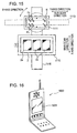
- the substrate and the inkjet head are preferably arranged as shown in Fig, 15 .
- reference numeral H7 denotes a support substrate for supporting a plurality of inkjet heads H1 mounted thereon.
- On an ink ejection surface (a surface opposite to the substrate) of the inkjet head H1 are provided a plurality of ejecting nozzles (for example, 180 nozzles in one column, the total of 360 nozzles) in two columns in the form of a column along the longitudinal direction of the head, with an interval in the width direction of the head.
- a plurality of inkjet heads H1 (6 in one column, the total of 12 in Fig. 14 ) are positioned and supported on a roughly rectangular supporting plate 20, when viewed from top, arranged in two columns in the form of a column approximately along an X axis direction at an inclined angle with respect to the X axis (or Y axis), with an interval in a Y axis direction.
- reference numeral 1115 denotes a stage for loading the substrate 2 and reference numeral 1116 denotes a guide rail for guiding the stage 1115 in the X axis direction (a main scan direction) in the figure.
- the head H is movable in the Y axis direction (a sub scan direction) in Fig. 15 by a guide rail 1113 via a supporting member 1111 and is rotable in a ⁇ axis direction in the figure to incline the inkjet head H1 at a predetermined angle with respect to the main scan direction.
- the inkjet head at an inclined angle with respect to the main scan direction, it is possible to correspond nozzle pitches to pixel pitches.
- the nozzle pitches can correspond to any pixel pitches.
- the substrate 2 shown in Fig. 15 has a structure where a plurality of chips is arranged on a mother substrate.
- one chip region corresponds to one display device.
- three display regions 2a are formed, however, the present invention is not limited to this.
- the head H is moved to the left side in Fig. 15 via the guide rail 1113 and the substrate 2 is moved to the top side in Fig. 15 via the guide rail 1116.
- the left display region 2a is coated with the liquid composition while scanning the substrate 2.
- the head H is moved to the right side of the figure and then a middle display region 2a is coated with the liquid composition. This process is also true of a right display region 2a.
- the head H shown in Fig. 14 and the inkjet apparatus shown in Fig. 15 are used not only in the hole injection/transport layer formation process but also in the light emitting layer formation process.
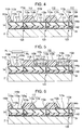
- the drying process as shown in Fig. 6 is performed.
- the first liquid composition after ejection is dried to evaporate the solvent included in the first liquid composition so as to form the hole injection/transport layer 110a.
- the evaporation of the solvent included in the liquid composition mainly occurs at a location near the inorganic bank layer 112a and the organic bank layer 112b, and, at the same time of evaporating the solvent, the hole injection/transport layer formation material is concentrated and educed. Accordingly, as shown in Fig. 6 , the peripheral portion 110a2 made of the hole injection/transport layer formation material is formed on the first stack portion 112e.
- the peripheral portion 110a2 is adhered closely to a wall surface (the organic bank layer 112b) of the upper opening 112d and has the thickness that is thin at a side near the electrode surface 111a and is thick at a side distant from the electrode surface 111a, i.e., a side near the organic bank layer 112b.
- the evaporation of the solvent also occurs on the electrode surface 111a by the drying process, and thus, the flat portion 110a1 made of the hole injection/transport layer formation material is formed on the electrode surface 111a. Since an evaporation speed of the solvent on the electrode surface 111a is nearly uniform, the hole injection/transport layer formation material is uniformly concentrated on the electrode surface 111a, and thus, the flat portion 110a1 having a uniform thickness is formed. In this way, the hole injection/transport layer 110a composed of the peripheral portion 110a2 and the flat portion 110a1 is formed. Alternatively, the hole injection/transport layer may not be formed on the peripheral portion 110a2, but may be formed on only the electrode surface 111a.
- the above-described drying process is performed at a room temperature under a pressure of, for example, 133.3 Pa (1 Torr) in a nitrogen atmosphere. If the pressure is too low, it is not preferable since the liquid droplets 110c of the liquid composition are abruptly boiled. In addition if temperature is high above the room temperature, a flat film may not be formed since an evaporation speed of a polar solvent becomes high. After the drying process, it is preferable to remove the polar solvent or water remaining in the hole injection/transport layer 110a by performing a thermal process, preferably, at a temperature of 200°C for ten minutes in a vacuum.
- the liquid composition bounces back from the lyophobic-processed organic bank layer 112b and rolls into the lower and upper openings 112c and 112d.
- the lower and upper openings 112c and 112d can be always filled with the ejected liquid droplets 110c of the liquid composition to form the hole injection/transport layer 110a on the electrode surface 111a.
- the light emitting layer formation process includes a light emitting layer formation material ejecting process and a drying process.
- the liquid composition for formation of the light emitting layer is ejected on the hole injection/transport layer 110a using the inkjet method. Thereafter, the ejected liquid composition is dried (and heated) to form the light emitting layer 110b on the hole injection/transport layer 110a.
- Fig. 7 shows an ejecting process of the liquid composition including the light emitting layer formation material using the inkjet method.
- the inkjet head H5 is moved in relation to the substrate 2, and the liquid composition containing the each color (here, for example, blue color (B)) light emitting layer formation material is ejected from the ejecting nozzles H6 formed in the inkjet head.
- the ejecting nozzles are opposite to the hole injection/transport layer 110a located within the lower and upper openings 112c and 112d and the inkjet head H5 is moved in relation to the substrate 2, the liquid composition is ejected.
- the amount of the liquid composition ejected from the ejecting nozzles H6 is controlled in such a manner that liquid measure per one drop is controlled.
- the liquid composition (liquid composition droplets 110e) having the controlled liquid measure is ejected on the hole injection/transport layer 110a from the ejecting nozzles.
- the liquid compositions for other light emitting layers are ejected.
- an arrangement operation for ejection of liquid composition droplets 110f and 110g is performed.
- a plurality of ejecting heads each of which is filled with the liquid composition for each color, may be independently scanned to arrange the liquid composition droplets 110e to 110g on the substrate 2, or alternatively, may be collectively scanned to arrange the liquid composition droplets 110e to 110f on the substrate 2 almost simultaneously.
- the ejected liquid compositions 110e to 110g are spread over the hole injection/transport layer 110a and are filled in the lower and upper openings 112c and 112d.
- the liquid composition droplet 110e to 110g are deviated from a predetermined ejection position and are ejected on the lyophobic-processed top surface 112f, the liquid composition droplet 110e to 110g roll into the lower and upper openings 112c and 112d without the top surface 112f wet by the liquid composition droplets 110e to 110g.
- the amount of liquid composition ejected on the hole injection/transport layer 110a depends on the size of the lower and upper openings 112c and 112d, the thickness of the light emitting layer 110b to be formed, the concentration of the light emitting layer formation material in the liquid composition, etc.
- the liquid compositions 110e to 110g may be ejected on the same hole injection/transport layer 110a not only one time but also multiple times. In this case, the amount of the liquid composition for each time may be equal or different.
- the liquid compositions may be ejected on not only the same location of the hole injection/transport layer 110a but also different locations of the hole injection/transport layer 110a for each time.
- polyfluorene high molecular derivatives As a formation material of the light emitting layer, polyfluorene high molecular derivatives, (poly) paraphenylenevinylene derivatives, polyphenylene derivatives, polyvinylcarbazole, polythiophene derivatives, perylene pigment, coumarin pigment, or rhodamine pigment can be used.
- these high molecular materials doped with organic EL materials such as rubrene, perylene, 9,10-diphenylanthracene, tetraphenylbutadiene, nile red, coumarin 6, or quinacridone can be used.
- the solvent for dissolving or dispersing these light emitting layer formation materials uses the same kind for each color light emitting layer.
- the film thickness of the light emitting layer may become ununiform due to the viscosity difference. Accordingly, in this embodiment, by making the surface area of the projecting portion 112e of the inorganic bank layer 112a different in advance for each light emitting layers 110b1 to 110b3 (i.e., for different color pixels), the light emitting layer is prevented or suppressed from having ununiform film thickness.
- the amount of projection of the projecting portion 112e becomes large to increase the surface area of the projecting portion 112e.
- the amount of projection of the projecting portion 112e becomes small to decrease the surface area of the projecting portion 112e.
- the light emitting layers 110b1 to 110b3 are formed by collectively drying the liquid compositions 110e to 110g.
- the solvent included in the liquid composition droplets 110e to 110g is evaporated by the drying process to thereby form the red color (R) light emitting layer 110b1, the green color (G) light emitting layer 110b2, and the blue color (B) light emitting layer 110b3, as shown in Fig. 9 .
- Fig. 9 shows the red, green and blue color light emitting layers one by one, since the light emitting elements are originally formed in the form of the matrix, as can be seen from Fig. 1 and other figures, a plurality if light emitting layers (corresponding to each color) (not shown) is formed.
- the liquid compositions of the light emitting layers are preferably dried by a vacuum drying process, more specifically, for example, at a room temperature at a pressure of 133.3 Pa (1 Torr) in a nitrogen atmosphere. If the pressure is too low, it is not preferable since the liquid compositions are abruptly boiled. In addition, if temperature is high above the room temperature, it is not preferable since an evaporation speed of the solvent becomes high, and accordingly, the light emitting layer formation material is much adhered to the wall surface of the upper opening 112d.
- the drying process is ended, it is preferable to perform an annealing process for the light emitting layer 110b using a heating means such as a hot plate.
- the annealing process is performed at a common temperature for a common time wherein light emission characteristics of organic EL layers can be obtained at maximum. In this way, the hole injection/transport layer 110a and the light emitting layer 110b are formed on the pixel electrode 111.
- a surface reforming process for reforming the surface of the hole injection/transport layer 110a may be performed prior to the light emitting layer formation material ejecting process.
- an insoluble solvent for the hole injection/transport layer 110a as the solvent of the liquid composition used in the light emitting layer formation process.
- the hole injection/transport layer 110a since the hole injection/transport layer 110a has low affinity to the solvent, even when the liquid compositions including the solvent are ejected on the hole injection/transport layer 110a, the hole injection/transport layer 110a may not be adhered closely to the light emitting layer 110b or the light emitting layer 110b may not uniformly coated with the liquid compositions. Accordingly, in order to increase the affinity of the surface of the hole injection/transport layer 110a to the solvent and the light emitting layer formation material, it is preferable to perform the surface reforming process before the light emitting layer formation process.
- the surface reforming process may be performed by coating a surface reforming material, which is equal or similar to the solvent of the liquid composition used in the light emitting layer formation process, on the hole injection/transport layer 110a using the inkjet method (liquid droplet ejecting method), a spin coat method, or a dip method and drying the coated surface reforming material.
- the surface reforming material used includes, for example, cyclohexyl benzene, isoprophyl biphenyl, trimethylbenzene, etc., which are equal to the solvent of the liquid composition, and includes, for example, tetramethylbenzenetoluene, toluene, xylene, etc., which are similar to the solvent of the liquid composition.
- the negative electrode 12 paired with the pixel electrode (positive electrode) 111 is formed.
- the negative electrode 12 composed of a calcium layer and an aluminum layer, which are stacked in order, is formed on the entire surface of the substrate 2 including the color light emitting layers 110b and the organic bank layer 112b.
- the negative electrode 12 is stacked on the entire region of the color light emitting layers 110b to form the organic EL elements corresponding to the red, green and blue colors.
- the negative electrode 12 is preferably formed by, for example, a deposition method, a sputtering method, a CVD method, etc. Particularly, it is preferable to form the negative electrode 12 using the deposition method since this method can prevent damage of the light emitting layers 110b due to heat. In addition, protective layers, such as SiO 2 or SiN, for anti-oxidation may be provided on the negative electrode 12.
- the substrate 2 having the organic EL elements formed thereon and a separately prepared sealing substrate are sealed via a sealing resin.
- the peripheral of the substrate 2 is coated with the sealing resin such as a thermosetting resin or an ultraviolet curing resin, and then, the sealing substrate is placed on the sealing resin.
- the sealing resin such as a thermosetting resin or an ultraviolet curing resin
- the organic EL device according to this embodiment is completed by connecting the negative electrode 12 to wiring lines of the substrate 2 and connecting wiring lines of the circuit element portion 14 to a driving IC (driving circuit), which is formed on the substrate 2 or provided in the outside.
- driving IC driving circuit
- the present invention is applicable to a manufacturing method of a color filter substrate on which coloring layers having a plurality of colors are arranged, or a manufacturing method of a device including a semiconductor device such as an organic TFT. Accordingly, it should be understood that, by such manufacturing methods of the color filter and the device, it is possible to obtain effects of enhancement of flatness of the coloring layers or other functional layers.
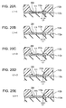
- the surface shape of the formed layer 200 is varied due to a viscosity difference. More specifically, the layer 200 has a U-shaped concave section when the viscosity is low ( Figs. 17(a) and 17(b) ), while the layer 200 has a reversed U-shaped convex section when the viscosity is high ( Figs. 17(e) and 17(d) ).
- the surface shape of the formed layer 200 is varied due to a projecting width L1 difference.
- the layer 200 has a U-shaped concave section when the projecting width L1 is large ( Fig. 18(a) ), while the layer 200 has a reversed U-shaped convex section when the projecting width L1 is small ( Fig. 18(e) ).
- the shape of the layer 200 can be controlled in various ways by the viscosity of the liquid compositions and the amount of projection of the projecting portion 112e (i.e., the area of the projecting portion 112e).
- the viscosity of the liquid compositions i.e., the area of the projecting portion 112e.
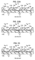
- the layer 200 having the flat surface shape can be formed. For example, as shown in Fig.
- a lower layer of the bank has a projecting shape, and a single functional layer is formed in the bank using the liquid droplet ejecting method
- flatness of the surface shape of the functional layer can be achieved as follows.
- a color filter is formed as the functional layer, when the viscosity of the liquid composition ejected using the liquid droplet ejecting method is common for the colors R, G and B in a process for forming a red color layer 200R, a green color layer 200G and a blue color layer 200B, a flat color filter can be obtained by making bank shapes for the colors R, G and B equal.
- the color layers 200R, 200G and 200B are formed of different materials, it is possible to unify the viscosities of the liquid compositions for the colors by using different kinds of solvents for each color, using solvents having different concentrations, or, if necessary, making the molecular weights of the materials of the color layers different for each color.
- the color layers 200R, 200G and 200B having the flat surface shape can be formed by setting the projecting widths of the projecting portions 112e of the lower layer (inorganic bank layer) 112a in the bank different for each color layer, as shown in Fig. 21(c) .
- the viscosity of the liquid composition depends on ejectability, solubility, components, etc. of the liquid composition, it is common that the viscosity of the liquid composition is different for different kinds of functional layers to be formed. In this case, as described above, by setting the projecting width of the lower layer (inorganic bank layer) of the bank composed of two layers to be different for each kind of functional layer, the functional layer having a flat surface shape and a uniform film thickness can be formed.
- the liquid compositions for forming the light emitting layers have different viscosities for each color layer under normal conditions (same solvent, same concentration). Meanwhile, since componential materials of the color layers are equal, the liquid compositions for forming the hole injection/transport layer 110a formed under the corresponding light emitting layer 110 has the same viscosity for each color layer under normal conditions (same solvent, same concentration) .
- the light emitting layers 110b1, 110b2 and 110b3 having the flat surface shape can be formed by setting the viscosities of the liquid compositions equal for each color, as shown in Fig. 22(b) .
- both the hole injection/transport layer 110a and the light emitting layer 110b can obtain a flat film shape by setting the viscosities of the liquid compositions to be equal.
- the liquid composition for each color includes the solvent of the same kind and the same concentration
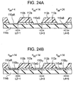
- the light emitting layers having the flat surface shape can be formed by setting the projecting widths of the inorganic bank layers 112a to be different for each color, as shown in Fig. 24 . More specifically, the projecting width L2 of the bank forming the red color light emitting layer is set to 1 ⁇ m, the projecting width L3 of the bank forming the green color light emitting layer is set to 3 ⁇ m, and the projecting width L4 of the bank forming the blue color light emitting layer is set to 5 ⁇ m.
- the hole injection/transport layer 110a having the flat surface shape can be obtained.
- the light emitting layers 110b1, 110b2 and 110b3 can be formed by ejecting the liquid compositions having the above-mentioned viscosities on the hole injection/transport layer 110a. Accordingly, the light emitting layer 110b having the flat surface shape can be obtained.
- Fig. 16 shows an embodiment of an electronic apparatus related to but not part of the present invention.
- the electronic apparatus according to this embodiment includes the above-described organic EL device as a display means.
- an example of a portable telephone is shown through a perspective view, where reference numeral 1000 denotes a portable telephone body and reference numeral 1001 denotes a display unit employing the organic EL device 1.
- the electronic apparatus including the organic EL device related to this embodiment as the display means can exhibit good light emission characteristics.
Landscapes
- Engineering & Computer Science (AREA)
- Manufacturing & Machinery (AREA)
- Electroluminescent Light Sources (AREA)
- Optical Filters (AREA)
- Devices For Indicating Variable Information By Combining Individual Elements (AREA)
- Application Of Or Painting With Fluid Materials (AREA)
Claims (4)
- Procédé de fabrication d'un dispositif électro-optique incluant différents types de couches électro-optiques selon un motif prédéterminé, le procédé comprenant :une étape de formation de parties de cloison pour former sur un substrat (2) une première partie de cloison (112a) ayant une première ouverture (112c) définissant une région dans laquelle les couches électro-optiques (110) sont formées et une deuxième partie de cloison (112b) située sur la première partie de cloison et ayant une deuxième ouverture (112d) définissant la région dans laquelle les couches électro-optiques sont formées ; etune étape d'éjection pour éjecter des substances liquides (110c) pour les ouvertures des parties de cloison en utilisant un procédé d'éjection de gouttelettes de liquide, les substances liquides étant obtenues par dissolution ou dispersion de matières fonctionnelles composant les couches électro-optiques respectives dans des solvants,caractérisé en ce que les substances liquides éjectées ont des viscosités plus élevées et plus basses pour chaque couche électro-optique, etdans lequel, à l'étape de formation de parties de cloison, la première partie de cloison se projette d'une surface intérieure de la deuxième ouverture de la deuxième partie de cloison, une superficie d'une partie (112e) de la première partie de cloison se projetant de la deuxième partie de cloison devient plus petite dans une ouverture, dans laquelle la substance liquide ayant une viscosité plus basse est éjectée, que la superficie de la partie de la première partie de cloison se projetant de la deuxième partie de cloison dans une ouverture à travers laquelle la substance liquide ayant une viscosité plus élevée est éjectée.
- Procédé de fabrication d'un dispositif électro-optique selon la revendication 1,
dans lequel, à l'étape de formation de parties de cloison, la longueur de projection de la première partie de cloison (112a) se projetant de la surface intérieure de la deuxième ouverture (112d) de la deuxième partie de cloison (112b) devient plus petite dans une ouverture dans laquelle la substance liquide ayant une viscosité plus basse est éjectée que la longueur de projection de la première partie de cloison se projetant de la deuxième partie de cloison dans une ouverture à travers laquelle la substance liquide ayant une viscosité plus élevée est éjectée. - Procédé de fabrication d'un dispositif électro-optique selon la revendication 1 ou 2,
dans lequel le solvant inclus dans la substance liquide (110c) est de la même espèce pour le même type de couches électro-optiques. - Procédé de fabrication d'un dispositif électro-optique selon l'une quelconque des revendications 1 à 3, comprenant en outre :après l'étape d'éjection, une étape de séchage pour sécher les substances liquides éjectées simultanément pour le même type de couches électro-optiques.
Applications Claiming Priority (4)
| Application Number | Priority Date | Filing Date | Title |
|---|---|---|---|
| JP2004157833 | 2004-05-27 | ||
| JP2004157833 | 2004-05-27 | ||
| JP2004288493 | 2004-09-30 | ||
| JP2004288493A JP4161956B2 (ja) | 2004-05-27 | 2004-09-30 | カラーフィルタ基板の製造方法、電気光学装置の製造方法、電気光学装置、電子機器 |
Publications (3)
| Publication Number | Publication Date |
|---|---|
| EP1601032A2 EP1601032A2 (fr) | 2005-11-30 |
| EP1601032A3 EP1601032A3 (fr) | 2009-10-14 |
| EP1601032B1 true EP1601032B1 (fr) | 2012-06-27 |
Family
ID=34934610
Family Applications (1)
| Application Number | Title | Priority Date | Filing Date |
|---|---|---|---|
| EP05007001A Expired - Fee Related EP1601032B1 (fr) | 2004-05-27 | 2005-03-31 | Impression par jet d'encre d'un panneau d'affichage organique électroluminescent |
Country Status (5)
| Country | Link |
|---|---|
| US (1) | US7244158B2 (fr) |
| EP (1) | EP1601032B1 (fr) |
| JP (1) | JP4161956B2 (fr) |
| KR (1) | KR100645484B1 (fr) |
| TW (1) | TWI264567B (fr) |
Cited By (2)
| Publication number | Priority date | Publication date | Assignee | Title |
|---|---|---|---|---|
| WO2014113079A1 (fr) * | 2013-01-17 | 2014-07-24 | Kateeva, Inc. | Dispositifs diodes électroluminescentes organiques haute résolution |
| US9444050B2 (en) | 2013-01-17 | 2016-09-13 | Kateeva, Inc. | High resolution organic light-emitting diode devices, displays, and related method |
Families Citing this family (55)
| Publication number | Priority date | Publication date | Assignee | Title |
|---|---|---|---|---|
| JP3841096B2 (ja) * | 2004-09-28 | 2006-11-01 | セイコーエプソン株式会社 | 配線パターンの形成方法、多層配線基板の製造方法、電子機器 |
| JP4297106B2 (ja) * | 2005-02-23 | 2009-07-15 | セイコーエプソン株式会社 | 膜パターンの形成方法及びデバイスの製造方法、電気光学装置及び電子機器 |
| JP4251331B2 (ja) * | 2005-12-27 | 2009-04-08 | カシオ計算機株式会社 | 表示装置の製造装置及び表示装置の製造方法 |
| KR101325577B1 (ko) * | 2006-04-28 | 2013-11-06 | 삼성디스플레이 주식회사 | 유기전계 발광소자 및 그 제조방법 |
| JP4957318B2 (ja) * | 2007-03-27 | 2012-06-20 | セイコーエプソン株式会社 | 有機el装置の製造方法 |
| JP5170020B2 (ja) | 2008-10-03 | 2013-03-27 | セイコーエプソン株式会社 | 有機el装置及び電子機器 |
| EP2398084B1 (fr) | 2009-02-10 | 2018-06-06 | Joled Inc. | Elément électroluminescent, dispositif électroluminescent comprenant l'élément électroluminescent et procédé de fabrication de l'élément électroluminescent |
| EP2398085B1 (fr) | 2009-02-10 | 2018-06-27 | Joled Inc. | Elément électroluminescent, dispositif d'affichage et procédé de fabrication d'un élément électroluminescent |
| JP5437736B2 (ja) | 2009-08-19 | 2014-03-12 | パナソニック株式会社 | 有機el素子 |
| JP2011210614A (ja) * | 2010-03-30 | 2011-10-20 | Toppan Printing Co Ltd | 有機el素子及びその製造方法 |
| JP5624141B2 (ja) * | 2010-07-30 | 2014-11-12 | パナソニック株式会社 | 有機el素子 |
| WO2012017495A1 (fr) * | 2010-08-06 | 2012-02-09 | パナソニック株式会社 | Elément el organique et procédé de fabrication associé |
| WO2012017485A1 (fr) * | 2010-08-06 | 2012-02-09 | パナソニック株式会社 | Élément électroluminescent organique, dispositif d'affichage et dispositif électroluminescent |
| WO2012017496A1 (fr) * | 2010-08-06 | 2012-02-09 | パナソニック株式会社 | Dispositif émetteur de lumière, appareil émettant de la lumière équipé dudit dispositif, et procédé de fabrication d'un dispositif émetteur de lumière |
| WO2012017502A1 (fr) * | 2010-08-06 | 2012-02-09 | パナソニック株式会社 | Élément électroluminescent organique et son procédé de fabrication |
| WO2012017503A1 (fr) * | 2010-08-06 | 2012-02-09 | パナソニック株式会社 | Élément électroluminescent organique |
| WO2012017486A1 (fr) | 2010-08-06 | 2012-02-09 | パナソニック株式会社 | Procédé de production d'éléments électroluminescents |
| WO2012017494A1 (fr) * | 2010-08-06 | 2012-02-09 | パナソニック株式会社 | Ecran d'affichage el organique, dispositif d'affichage, et procédé pour fabriquer un écran d'affichage el organique |
| WO2012017501A1 (fr) * | 2010-08-06 | 2012-02-09 | パナソニック株式会社 | Élément électroluminescent organique et son procédé de fabrication |
| JP5574456B2 (ja) | 2010-08-06 | 2014-08-20 | パナソニック株式会社 | 発光素子とその製造方法、および発光装置 |
| JP5658256B2 (ja) * | 2010-08-06 | 2015-01-21 | パナソニック株式会社 | 発光素子とその製造方法、および発光装置 |
| JP5543600B2 (ja) | 2010-08-06 | 2014-07-09 | パナソニック株式会社 | 発光素子、発光素子を備えた発光装置および発光素子の製造方法 |
| WO2012017497A1 (fr) | 2010-08-06 | 2012-02-09 | パナソニック株式会社 | Elément el organique |
| JP5677432B2 (ja) * | 2010-08-06 | 2015-02-25 | パナソニック株式会社 | 有機el素子、表示装置および発光装置 |
| WO2012017490A1 (fr) * | 2010-08-06 | 2012-02-09 | パナソニック株式会社 | Élément électroluminescent organique, dispositif d'affichage et dispositif électroluminescent |
| WO2012017499A1 (fr) * | 2010-08-06 | 2012-02-09 | パナソニック株式会社 | Élément électroluminescent organique |
| JP2012099458A (ja) * | 2010-10-05 | 2012-05-24 | Seiko Epson Corp | 有機el照明装置およびその製造方法 |
| JP5676652B2 (ja) | 2011-01-21 | 2015-02-25 | パナソニック株式会社 | 有機el素子 |
| CN103314462B (zh) | 2011-02-23 | 2016-03-02 | 株式会社日本有机雷特显示器 | 有机el显示面板和有机el显示装置 |
| JP5809234B2 (ja) | 2011-02-25 | 2015-11-10 | 株式会社Joled | 有機el表示パネルおよび有機el表示装置 |
| CN102884650A (zh) | 2011-05-11 | 2013-01-16 | 松下电器产业株式会社 | 有机el显示面板及有机el显示装置 |
| US20140363911A1 (en) * | 2011-12-15 | 2014-12-11 | Panasonic Corporation | Method for producing organic el display panel |
| JPWO2013088744A1 (ja) * | 2011-12-15 | 2015-04-27 | パナソニック株式会社 | 有機el表示パネルの製造方法 |
| JP5899531B2 (ja) * | 2012-01-12 | 2016-04-06 | 株式会社Joled | 有機el素子の製造方法 |
| JP6082974B2 (ja) * | 2012-08-09 | 2017-02-22 | 株式会社Joled | 有機膜の製造方法と有機elパネルの製造方法 |
| KR102011873B1 (ko) * | 2013-05-02 | 2019-10-22 | 삼성디스플레이 주식회사 | 유기 발광 표시 장치의 제조 방법 |
| KR102205700B1 (ko) * | 2014-07-16 | 2021-01-21 | 삼성전자주식회사 | 유기 전계발광 표시장치 및 그 제조 방법 |
| CN104465708B (zh) * | 2014-12-24 | 2017-10-17 | 京东方科技集团股份有限公司 | 一种阵列基板及其制作方法和显示装置 |
| KR102377490B1 (ko) * | 2015-03-24 | 2022-03-22 | 삼성디스플레이 주식회사 | 발광 표시 장치 및 그 제조 방법 |
| KR102457536B1 (ko) * | 2015-06-30 | 2022-10-21 | 엘지디스플레이 주식회사 | 유기전계발광표시장치 |
| KR102467213B1 (ko) * | 2015-07-28 | 2022-11-15 | 엘지디스플레이 주식회사 | 유기발광다이오드 표시장치 |
| JP6575239B2 (ja) | 2015-09-02 | 2019-09-18 | セイコーエプソン株式会社 | 機能素子の製造方法 |
| KR102702122B1 (ko) * | 2016-07-29 | 2024-09-02 | 엘지디스플레이 주식회사 | 표시장치 |
| KR102550693B1 (ko) * | 2016-08-04 | 2023-07-04 | 삼성디스플레이 주식회사 | 플렉시블 디스플레이 장치 및 제조 방법 |
| JP6686787B2 (ja) * | 2016-08-12 | 2020-04-22 | 株式会社デンソー | 有機el表示装置およびその製造方法 |
| TWI763772B (zh) * | 2017-01-30 | 2022-05-11 | 德商麥克專利有限公司 | 電子裝置之有機元件的形成方法 |
| CN106920828B (zh) * | 2017-03-29 | 2019-11-05 | 京东方科技集团股份有限公司 | 一种有机电致发光显示面板及制备方法 |
| CN109860223B (zh) * | 2017-11-30 | 2021-01-22 | 京东方科技集团股份有限公司 | 像素界定层、显示基板、显示装置、喷墨打印方法 |
| KR102577043B1 (ko) * | 2017-12-11 | 2023-09-08 | 엘지디스플레이 주식회사 | 전계발광 표시장치 |
| KR102495204B1 (ko) * | 2017-12-29 | 2023-02-01 | 엘지디스플레이 주식회사 | Oled 표시장치 |
| KR102710587B1 (ko) * | 2019-09-04 | 2024-09-26 | 삼성디스플레이 주식회사 | 표시 장치 |
| EP3845976B1 (fr) * | 2019-12-30 | 2024-03-20 | The Swatch Group Research and Development Ltd | Cadran de montre ayant un affichage à base de diodes électroluminescentes organiques |
| CN111769143B (zh) * | 2020-06-23 | 2022-09-09 | 武汉华星光电半导体显示技术有限公司 | 显示面板及其制造方法 |
| KR102936537B1 (ko) * | 2021-10-07 | 2026-03-10 | 삼성디스플레이 주식회사 | 표시 장치 |
| KR20230101618A (ko) * | 2021-12-29 | 2023-07-06 | 엘지디스플레이 주식회사 | 유기 발광 표시 패널 및 그의 제조 방법 |
Family Cites Families (11)
| Publication number | Priority date | Publication date | Assignee | Title |
|---|---|---|---|---|
| US3445666A (en) * | 1964-10-26 | 1969-05-20 | Alvin A Snaper | Electro-optical device with concentric arrangement of layers |
| WO1999048339A1 (fr) | 1998-03-17 | 1999-09-23 | Seiko Epson Corporation | Substrat de formation de motifs sur film mince et son traitement de surface |
| JP3628997B2 (ja) * | 2000-11-27 | 2005-03-16 | セイコーエプソン株式会社 | 有機エレクトロルミネッセンス装置の製造方法 |
| JP4042692B2 (ja) | 2000-11-27 | 2008-02-06 | セイコーエプソン株式会社 | 有機エレクトロルミネッセンス装置の製造方法 |
| JP4042409B2 (ja) | 2000-11-27 | 2008-02-06 | セイコーエプソン株式会社 | 有機エレクトロルミネッセンス装置 |
| JP4042691B2 (ja) | 2000-11-27 | 2008-02-06 | セイコーエプソン株式会社 | 有機エレクトロルミネッセンス装置の製造方法 |
| JP3823916B2 (ja) * | 2001-12-18 | 2006-09-20 | セイコーエプソン株式会社 | 表示装置及び電子機器並びに表示装置の製造方法 |
| JP2003249378A (ja) | 2001-12-18 | 2003-09-05 | Seiko Epson Corp | 表示装置及び電子機器 |
| JP2003249377A (ja) | 2001-12-18 | 2003-09-05 | Seiko Epson Corp | 表示装置及び電子機器並びに表示装置の製造方法 |
| JP3705264B2 (ja) | 2001-12-18 | 2005-10-12 | セイコーエプソン株式会社 | 表示装置及び電子機器 |
| JP4014901B2 (ja) * | 2002-03-14 | 2007-11-28 | セイコーエプソン株式会社 | 液滴吐出による材料の配置方法および表示装置の製造方法 |
-
2004
- 2004-09-30 JP JP2004288493A patent/JP4161956B2/ja not_active Expired - Fee Related
-
2005
- 2005-03-29 KR KR1020050025782A patent/KR100645484B1/ko not_active Expired - Fee Related
- 2005-03-31 EP EP05007001A patent/EP1601032B1/fr not_active Expired - Fee Related
- 2005-04-08 TW TW094111221A patent/TWI264567B/zh not_active IP Right Cessation
- 2005-04-19 US US11/108,781 patent/US7244158B2/en not_active Expired - Fee Related
Cited By (11)
| Publication number | Priority date | Publication date | Assignee | Title |
|---|---|---|---|---|
| WO2014113079A1 (fr) * | 2013-01-17 | 2014-07-24 | Kateeva, Inc. | Dispositifs diodes électroluminescentes organiques haute résolution |
| US9444050B2 (en) | 2013-01-17 | 2016-09-13 | Kateeva, Inc. | High resolution organic light-emitting diode devices, displays, and related method |
| US9614191B2 (en) | 2013-01-17 | 2017-04-04 | Kateeva, Inc. | High resolution organic light-emitting diode devices, displays, and related methods |
| US9666652B2 (en) | 2013-01-17 | 2017-05-30 | Kateeva, Inc. | High resolution organic light-emitting diode devices, displays, and related method |
| US10269874B2 (en) | 2013-01-17 | 2019-04-23 | Kateeva, Inc. | High resolution organic light-emitting diode devices, displays, and related methods |
| US10522601B2 (en) | 2013-01-17 | 2019-12-31 | Kateeva, Inc. | High resolution organic light-emitting diode devices, displays, and related method |
| US10580841B2 (en) | 2013-01-17 | 2020-03-03 | Kateeva, Inc. | High resolution organic light-emitting diode devices, displays, and related method |
| US10707273B2 (en) | 2013-01-17 | 2020-07-07 | Kateeva, Inc. | High resolution organic light-emitting diode devices, displays, and related methods |
| US10985217B2 (en) | 2013-01-17 | 2021-04-20 | Kateeva, Inc. | High resolution organic light-emitting diode devices, displays, and related methods |
| US11489019B2 (en) | 2013-01-17 | 2022-11-01 | Kateeva, Inc. | High resolution organic light-emitting diode devices, displays, and related methods |
| US12167663B2 (en) | 2013-01-17 | 2024-12-10 | Kateeva, Inc. | High resolution organic light-emitting diode devices, displays, and related methods |
Also Published As
| Publication number | Publication date |
|---|---|
| KR100645484B1 (ko) | 2006-11-14 |
| JP2006012762A (ja) | 2006-01-12 |
| EP1601032A2 (fr) | 2005-11-30 |
| TWI264567B (en) | 2006-10-21 |
| US7244158B2 (en) | 2007-07-17 |
| JP4161956B2 (ja) | 2008-10-08 |
| US20050266763A1 (en) | 2005-12-01 |
| EP1601032A3 (fr) | 2009-10-14 |
| TW200604588A (en) | 2006-02-01 |
| KR20060044885A (ko) | 2006-05-16 |
Similar Documents
| Publication | Publication Date | Title |
|---|---|---|
| EP1601032B1 (fr) | Impression par jet d'encre d'un panneau d'affichage organique électroluminescent | |
| KR100506353B1 (ko) | 표시 장치 및 전자 기기, 표시 장치의 제조 방법 | |
| JP4055171B2 (ja) | カラーフィルタ基板の製造方法、電気光学装置の製造方法、電気光学装置、電子機器 | |
| JP4556604B2 (ja) | 表示装置の製造方法及び電子機器の製造方法 | |
| US8029850B2 (en) | Method of manufacturing organic electroluminescent device and method of manufacturing device | |
| KR100645485B1 (ko) | 표시 장치, 표시 장치의 제조 방법 및 전자 기기 | |
| JP2003249376A (ja) | 表示装置及び電子機器 | |
| JP2004355913A (ja) | 有機エレクトロルミネッセンス装置の製造方法 | |
| JP2006252988A (ja) | エレクトロルミネッセンス装置、電子機器 | |
| JP4715226B2 (ja) | 有機エレクトロルミネッセンス装置、有機エレクトロルミネッセンス装置の製造方法、電子機器 | |
| JP2003187970A (ja) | 表示装置の製造方法、電子機器の製造方法、表示装置および電子機器 | |
| JP4595387B2 (ja) | 液滴吐出装置、液滴吐出方法、カラーフィルタ基板の製造方法、電気光学装置の製造方法 | |
| CN100490213C (zh) | 滤色片基板的制造方法、电光学装置及其制造方法、电子设备 | |
| JP2003249378A (ja) | 表示装置及び電子機器 | |
| JP2004200158A (ja) | 有機el装置製造用基板、有機el装置、有機el装置の製造方法、及び電子機器 | |
| JP4788144B2 (ja) | 発光装置の製造方法 | |
| JP5304417B2 (ja) | 表示装置 | |
| KR20060049804A (ko) | 표시 장치 및 전자 기기 | |
| JP2003249377A (ja) | 表示装置及び電子機器並びに表示装置の製造方法 | |
| JP4752303B2 (ja) | El装置の製造方法、el装置、電子機器 | |
| JP2006041003A (ja) | 表示装置、電子機器 | |
| JP2006038986A (ja) | 表示装置、電子機器 | |
| JP2005353528A (ja) | 電気光学装置の製造方法、電気光学装置、電子機器 | |
| JP2003217843A (ja) | 表示装置の製造方法、電子機器の製造方法、表示装置および電子機器 | |
| JP2006278127A (ja) | デバイスの製造方法、el装置の製造方法、el装置、電子機器 |
Legal Events
| Date | Code | Title | Description |
|---|---|---|---|
| PUAI | Public reference made under article 153(3) epc to a published international application that has entered the european phase |
Free format text: ORIGINAL CODE: 0009012 |
|
| AK | Designated contracting states |
Kind code of ref document: A2 Designated state(s): AT BE BG CH CY CZ DE DK EE ES FI FR GB GR HU IE IS IT LI LT LU MC NL PL PT RO SE SI SK TR |
|
| AX | Request for extension of the european patent |
Extension state: AL BA HR LV MK YU |
|
| PUAL | Search report despatched |
Free format text: ORIGINAL CODE: 0009013 |
|
| AK | Designated contracting states |
Kind code of ref document: A3 Designated state(s): AT BE BG CH CY CZ DE DK EE ES FI FR GB GR HU IE IS IT LI LT LU MC NL PL PT RO SE SI SK TR |
|
| AX | Request for extension of the european patent |
Extension state: AL BA HR LV MK YU |
|
| RIC1 | Information provided on ipc code assigned before grant |
Ipc: H01L 27/00 20060101ALI20050830BHEP Ipc: H01L 51/00 20060101AFI20090909BHEP |
|
| 17P | Request for examination filed |
Effective date: 20100318 |
|
| 17Q | First examination report despatched |
Effective date: 20100419 |
|
| AKX | Designation fees paid |
Designated state(s): DE FR GB |
|
| GRAP | Despatch of communication of intention to grant a patent |
Free format text: ORIGINAL CODE: EPIDOSNIGR1 |
|
| GRAS | Grant fee paid |
Free format text: ORIGINAL CODE: EPIDOSNIGR3 |
|
| GRAA | (expected) grant |
Free format text: ORIGINAL CODE: 0009210 |
|
| AK | Designated contracting states |
Kind code of ref document: B1 Designated state(s): DE FR GB |
|
| REG | Reference to a national code |
Ref country code: GB Ref legal event code: FG4D |
|
| REG | Reference to a national code |
Ref country code: DE Ref legal event code: R096 Ref document number: 602005034906 Country of ref document: DE Effective date: 20120823 |
|
| PLBE | No opposition filed within time limit |
Free format text: ORIGINAL CODE: 0009261 |
|
| STAA | Information on the status of an ep patent application or granted ep patent |
Free format text: STATUS: NO OPPOSITION FILED WITHIN TIME LIMIT |
|
| 26N | No opposition filed |
Effective date: 20130328 |
|
| REG | Reference to a national code |
Ref country code: DE Ref legal event code: R097 Ref document number: 602005034906 Country of ref document: DE Effective date: 20130328 |
|
| REG | Reference to a national code |
Ref country code: FR Ref legal event code: PLFP Year of fee payment: 11 |
|
| PGFP | Annual fee paid to national office [announced via postgrant information from national office to epo] |
Ref country code: DE Payment date: 20150324 Year of fee payment: 11 |
|
| PGFP | Annual fee paid to national office [announced via postgrant information from national office to epo] |
Ref country code: GB Payment date: 20150325 Year of fee payment: 11 Ref country code: FR Payment date: 20150309 Year of fee payment: 11 |
|
| REG | Reference to a national code |
Ref country code: DE Ref legal event code: R119 Ref document number: 602005034906 Country of ref document: DE |
|
| GBPC | Gb: european patent ceased through non-payment of renewal fee |
Effective date: 20160331 |
|
| REG | Reference to a national code |
Ref country code: FR Ref legal event code: ST Effective date: 20161130 |
|
| PG25 | Lapsed in a contracting state [announced via postgrant information from national office to epo] |
Ref country code: GB Free format text: LAPSE BECAUSE OF NON-PAYMENT OF DUE FEES Effective date: 20160331 Ref country code: FR Free format text: LAPSE BECAUSE OF NON-PAYMENT OF DUE FEES Effective date: 20160331 Ref country code: DE Free format text: LAPSE BECAUSE OF NON-PAYMENT OF DUE FEES Effective date: 20161001 |