WO2012017497A1 - Elément el organique - Google Patents
Elément el organique Download PDFInfo
- Publication number
- WO2012017497A1 WO2012017497A1 PCT/JP2010/004987 JP2010004987W WO2012017497A1 WO 2012017497 A1 WO2012017497 A1 WO 2012017497A1 JP 2010004987 W JP2010004987 W JP 2010004987W WO 2012017497 A1 WO2012017497 A1 WO 2012017497A1
- Authority
- WO
- WIPO (PCT)
- Prior art keywords
- layer
- organic
- hole injection
- bank
- injection layer
- Prior art date
- Legal status (The legal status is an assumption and is not a legal conclusion. Google has not performed a legal analysis and makes no representation as to the accuracy of the status listed.)
- Ceased
Links
Images


Classifications
-
- H—ELECTRICITY
- H05—ELECTRIC TECHNIQUES NOT OTHERWISE PROVIDED FOR
- H05B—ELECTRIC HEATING; ELECTRIC LIGHT SOURCES NOT OTHERWISE PROVIDED FOR; CIRCUIT ARRANGEMENTS FOR ELECTRIC LIGHT SOURCES, IN GENERAL
- H05B33/00—Electroluminescent light sources
- H05B33/12—Light sources with substantially two-dimensional [2D] radiating surfaces
- H05B33/22—Light sources with substantially two-dimensional [2D] radiating surfaces characterised by the chemical or physical composition or the arrangement of auxiliary dielectric or reflective layers
-
- H—ELECTRICITY
- H10—SEMICONDUCTOR DEVICES; ELECTRIC SOLID-STATE DEVICES NOT OTHERWISE PROVIDED FOR
- H10K—ORGANIC ELECTRIC SOLID-STATE DEVICES
- H10K50/00—Organic light-emitting devices
- H10K50/10—OLEDs or polymer light-emitting diodes [PLED]
- H10K50/17—Carrier injection layers
-
- H—ELECTRICITY
- H10—SEMICONDUCTOR DEVICES; ELECTRIC SOLID-STATE DEVICES NOT OTHERWISE PROVIDED FOR
- H10K—ORGANIC ELECTRIC SOLID-STATE DEVICES
- H10K50/00—Organic light-emitting devices
- H10K50/80—Constructional details
- H10K50/805—Electrodes
- H10K50/81—Anodes
- H10K50/813—Anodes characterised by their shape
-
- H—ELECTRICITY
- H10—SEMICONDUCTOR DEVICES; ELECTRIC SOLID-STATE DEVICES NOT OTHERWISE PROVIDED FOR
- H10K—ORGANIC ELECTRIC SOLID-STATE DEVICES
- H10K50/00—Organic light-emitting devices
- H10K50/80—Constructional details
- H10K50/805—Electrodes
- H10K50/81—Anodes
- H10K50/818—Reflective anodes, e.g. ITO combined with thick metallic layers
-
- H—ELECTRICITY
- H10—SEMICONDUCTOR DEVICES; ELECTRIC SOLID-STATE DEVICES NOT OTHERWISE PROVIDED FOR
- H10K—ORGANIC ELECTRIC SOLID-STATE DEVICES
- H10K59/00—Integrated devices, or assemblies of multiple devices, comprising at least one organic light-emitting element covered by group H10K50/00
- H10K59/80—Constructional details
- H10K59/805—Electrodes
- H10K59/8051—Anodes
- H10K59/80515—Anodes characterised by their shape
-
- H—ELECTRICITY
- H10—SEMICONDUCTOR DEVICES; ELECTRIC SOLID-STATE DEVICES NOT OTHERWISE PROVIDED FOR
- H10K—ORGANIC ELECTRIC SOLID-STATE DEVICES
- H10K59/00—Integrated devices, or assemblies of multiple devices, comprising at least one organic light-emitting element covered by group H10K50/00
- H10K59/80—Constructional details
- H10K59/805—Electrodes
- H10K59/8051—Anodes
- H10K59/80518—Reflective anodes, e.g. ITO combined with thick metallic layers
-
- H—ELECTRICITY
- H10—SEMICONDUCTOR DEVICES; ELECTRIC SOLID-STATE DEVICES NOT OTHERWISE PROVIDED FOR
- H10K—ORGANIC ELECTRIC SOLID-STATE DEVICES
- H10K2102/00—Constructional details relating to the organic devices covered by this subclass
- H10K2102/301—Details of OLEDs
- H10K2102/331—Nanoparticles used in non-emissive layers, e.g. in packaging layer
-
- H—ELECTRICITY
- H10—SEMICONDUCTOR DEVICES; ELECTRIC SOLID-STATE DEVICES NOT OTHERWISE PROVIDED FOR
- H10K—ORGANIC ELECTRIC SOLID-STATE DEVICES
- H10K71/00—Manufacture or treatment specially adapted for the organic devices covered by this subclass
-
- H—ELECTRICITY
- H10—SEMICONDUCTOR DEVICES; ELECTRIC SOLID-STATE DEVICES NOT OTHERWISE PROVIDED FOR
- H10K—ORGANIC ELECTRIC SOLID-STATE DEVICES
- H10K71/00—Manufacture or treatment specially adapted for the organic devices covered by this subclass
- H10K71/10—Deposition of organic active material
- H10K71/12—Deposition of organic active material using liquid deposition, e.g. spin coating
- H10K71/13—Deposition of organic active material using liquid deposition, e.g. spin coating using printing techniques, e.g. ink-jet printing or screen printing
- H10K71/135—Deposition of organic active material using liquid deposition, e.g. spin coating using printing techniques, e.g. ink-jet printing or screen printing using ink-jet printing
Definitions
- the present invention relates to an organic electroluminescent element (hereinafter referred to as “organic EL element”) that is an electroluminescent element, and in particular, a technique for driving a wide luminance range from low luminance to high luminance such as a light source with low power. About.
- organic EL element organic electroluminescent element
- the organic EL element is a current-driven light-emitting element and has a configuration in which a functional layer containing an organic material is provided between a pair of electrodes including an anode and a cathode.
- the functional layer includes a light emitting layer, a buffer layer, and the like.
- a hole injection layer for injecting holes may be disposed between the functional layer and the anode.
- For driving a voltage is applied between the electrode pair, and an electroluminescence phenomenon generated by recombination of holes injected from the anode into the functional layer and electrons injected from the cathode into the functional layer is used. Since it is self-luminous, its visibility is high, and since it is a complete solid element, it has excellent impact resistance. Therefore, its use as a light-emitting element and a light source in various display devices has attracted attention.
- Organic EL elements are roughly classified into two types depending on the type of functional layer material used.
- the first is a vapor deposition type organic EL device in which a low molecular material is mainly used as a functional layer material and is formed by a vacuum process such as a vapor deposition method.
- a coating-type organic EL element is formed by using a high molecular material or a low molecular material having good thin film formability as a functional layer material, and forming the film by a wet process such as an inkjet method or a gravure printing method.
- the vapor deposition type organic EL element is suitable for a small-sized organic EL panel, but it is very difficult to apply it to, for example, a 100-inch class full-color large-sized organic EL panel.
- the factor lies in manufacturing technology.
- a mask vapor deposition method is generally used when forming a light emitting layer separately for each color (for example, R, G, B).
- R, G, B a color that is a mask vapor deposition method for each color
- the panel has a large area, it becomes difficult to maintain the alignment accuracy of the mask due to the difference in thermal expansion coefficient between the mask and the glass substrate, and thus a normal display cannot be manufactured.
- the functional layer material is produced by a wet process.
- the positional accuracy when the functional layer is separately applied to a predetermined position does not basically depend on the substrate size, there is a merit that a technical barrier against an increase in size is low.
- the present invention has been made in view of the above problems, and has a low hole injection barrier between the hole injection layer and the functional layer, and exhibits excellent hole injection efficiency.
- An object is to provide an organic EL element that can be expected.
- one embodiment of the present invention includes an anode, a cathode, and one or more layers including a light-emitting layer that is disposed between the anode and the cathode and uses an organic material.
- the hole injection layer includes tungsten oxide. Further, the hole injection layer is configured to have an occupied level in a binding energy region that is 1.8 to 3.6 eV lower than the lowest binding energy in the valence band in its electronic state. The existence of this occupied level can suppress the hole injection barrier between the hole injection layer and the functional layer. As a result, the organic EL element of one embodiment of the present invention has high hole injection efficiency, can be driven at a low voltage, and can be expected to exhibit excellent light emission efficiency.
- the hole injection layer is made of tungsten oxide having the above-mentioned predetermined occupation level
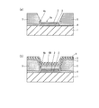
- the film thickness of the hole injection layer is reduced in the manufacturing process (hereinafter also referred to as film reduction). This may cause a problem and may affect the light emission characteristics such as luminance variation in the surface of the light emitting portion in the area defined by the bank and a decrease in element lifetime.
- the hole injection layer is formed in a concave structure in which a part of the surface on the functional layer side is located on the anode side with respect to the other surface part, Since the edge of the recessed structure of the hole injection layer is covered with a part of the bank, the electric field concentration at the edge can be reduced. As a result, problems such as luminance variations and a decrease in element lifetime can be prevented, and the influence on the light emission characteristics can be prevented beforehand.
- FIG. 1 is a schematic cross-sectional view showing a configuration of an organic EL element according to Embodiment 1.
- FIG. It is typical sectional drawing which shows the structure of a hole only element. It is a graph which shows the dependence of the drive voltage of a hole only element with respect to the film-forming conditions of a hole injection layer. It is a device characteristic figure which shows the relationship curve of the applied voltage and current density of a Hall only element. It is a device characteristic figure which shows the relationship curve of the applied voltage and current density of the produced organic EL element. It is a device characteristic figure which shows the relational curve of the current density of the produced organic EL element, and emitted light intensity. It is typical sectional drawing which shows the structure of the sample for photoelectron spectroscopy measurements.
- FIG. 6 is an end view for explaining a process for obtaining one embodiment of the present invention.
- FIG. 19 is an enlarged end view of a B portion surrounded by a one-dot chain line in FIG. 18. It is process drawing explaining the manufacturing method of the organic EL display which concerns on Embodiment 2 of this invention. It is process drawing explaining the manufacturing method of the organic EL display which concerns on Embodiment 2 of this invention. It is process drawing explaining the manufacturing method of the organic EL display which concerns on Embodiment 2 of this invention. It is process drawing explaining the manufacturing method of the organic EL display which concerns on Embodiment 2 of this invention.
- the organic EL element which is one embodiment of the present invention includes an anode, a cathode, a functional layer that is disposed between the anode and the cathode, and includes a light-emitting layer that uses an organic material. And a hole injecting layer disposed between the anode and the functional layer, and a bank defining the light emitting layer, the hole injecting layer comprising tungsten oxide and having the lowest bonding in the valence band Having an occupied level in a binding energy region 1.8 to 3.6 eV lower than the energy, and in the region defined by the bank, a part of the surface on the functional layer side is closer to the anode side than the other part. It is formed in the recessed structure located, and the edge of the recessed part in the said recessed structure is coat
- the binding energy of the highest occupied orbit of the functional layer at the stacked interface between the hole injection layer and the functional layer is the binding energy of the occupied level. It may be positioned in the vicinity of.
- the difference between the binding energy of the occupied level and the binding energy of the highest occupied orbit of the functional layer is within ⁇ 0.3 eV at the stacked interface between the hole injection layer and the functional layer. But you can.
- the hole injection layer has a raised shape in a binding energy region 1.8 to 3.6 eV lower than the lowest binding energy in the valence band in the UPS spectrum. Also good.
- the hole injection layer may have a raised shape in a binding energy region lower by 1.8 to 3.6 eV than the lowest binding energy in the valence band in the XPS spectrum.
- the hole injection layer is different from an exponential function over a binding energy region that is 2.0 to 3.2 eV lower than the lowest binding energy in the valence band in the differential spectrum of the UPS spectrum. It may have a shape expressed as a function.
- the functional layer may contain an amine-based material.
- the functional layer may be at least one of a hole transport layer that transports holes, a buffer layer that is used for optical property adjustment or electronic block application.
- the occupied level in the hole injection layer may exist in a binding energy region that is 2.0 to 3.2 eV lower than the lowest binding energy in the valence band.
- a part of the bank reaches the bottom surface of the recess in the recessed structure of the hole injection layer, and the side surface of the bank is an upward slope from the point of arrival to the bottom surface of the recess. It is good also as composition which becomes.
- a part of the bank may not reach the bottom surface of the concave portion in the concave structure of the hole injection layer.
- the hole injection layer may extend to the side of the bank along the bottom surface of the bank.
- the edge of the concave portion of the hole injection layer is a convex corner portion formed by a region that is not recessed on the upper surface of the hole injection layer and a side surface of the concave portion.
- the bank may be liquid repellent and the hole injection layer may be lyophilic.
- a display device that is an aspect of the present invention may include the organic EL element.
- a method for manufacturing an organic EL element is a step of forming a tungsten oxide layer on the positive anode, and is composed of argon gas and oxygen gas.
- the total pressure of the gas is more than 2.7 Pa and 7.0 Pa or less, and the ratio of the oxygen gas partial pressure to the total pressure is 50% or more and 70% or less.
- the tungsten oxide layer has a UPS spectrum that is lower than the lowest binding energy in the valence band by the second step.
- the film may be formed so as to have a raised shape in a low binding energy region of .8 to 3.6 eV.
- the differential spectrum of the UPS spectrum is 2.0 to 3.2 eV lower than the lowest binding energy in the valence band.
- the tungsten oxide layer may be formed so as to have a shape expressed as a function different from the exponential function over the region.
- FIG. 1 is a schematic cross-sectional view showing the configuration of the organic EL element 1000 in the present embodiment.
- the organic EL element 1000 is a coating type that is manufactured by applying a functional layer by a wet process, and includes a hole injection layer 4 and various functional layers (here, the buffer layer 6A and the organic layer having an organic material having a predetermined function). In the state where the light emitting layer 6B) is laminated with each other, the light emitting layer 6B) is interposed between the electrode pair composed of the anode 2 and the cathode 8.
- the organic EL element 1000 includes an anode 2, a hole injection layer 4, a buffer layer 6A, a light emitting layer 6B, a cathode 8 (barium layer 8A and aluminum) with respect to one main surface of the substrate 1.
- Layer 8B) in the same order.
- the substrate 1 is, for example, soda glass, non-fluorescent glass, phosphate glass, borate glass, quartz, acrylic resin, styrene resin, polycarbonate resin, epoxy resin, polyethylene, polyester, silicone resin, or alumina.
- the insulating material is used.
- a predetermined TFT wiring is formed on one surface thereof.
- the anode 2 is made of, for example, APC (silver, palladium, copper alloy), ARA (silver, rubidium, gold alloy), MoCr (molybdenum and chromium alloy), NiCr (nickel and chromium alloy), or the like. Can do. In the case of a top emission type light emitting element, it is preferably formed of a light reflective material.
- the hole injection layer 4 is made of a tungsten oxide thin film (layer) having a thickness of 30 nm. In the composition formula (WOx), x is a real number in the range of 2 ⁇ x ⁇ 3.
- the hole injection layer 4 is preferably composed of tungsten oxide as much as possible, but may contain a trace amount of impurities to such an extent that it can be mixed at a normal level.
- the hole injection layer 4 is formed under specific film formation conditions.
- an occupied level exists in a binding energy region that is 1.8 to 3.6 eV lower than the upper end of the valence band, that is, the lowest binding energy in the valence band.
- This occupied level corresponds to the highest occupied level of the hole injection layer 4, that is, its binding energy range is closest to the Fermi surface of the hole injection layer 4. Therefore, hereinafter, this occupied level is referred to as “occupied level near the Fermi surface”.
- substantially equal and “interface state connection is made” here means that the lowest binding energy at the occupied level near the Fermi surface at the interface between the hole injection layer 4 and the buffer layer 6A. This means that the difference from the lowest binding energy in the highest occupied orbit is within a range of ⁇ 0.3 eV.
- the “interface” here refers to a region including the surface of the hole injection layer 4 and the buffer layer 6A at a distance within 0.3 nm from the surface.
- the occupied level in the vicinity of the Fermi surface is preferably present in the whole hole injection layer 4, but may be present at least at the interface with the buffer layer 6A.
- a bank 5 made of an insulating organic material for example, an acrylic resin, a polyimide resin, a novolac type phenol resin, or the like
- a buffer layer 6A and a functional layer composed of a light emitting layer 6B corresponding to one of RGB colors are formed.
- a series of three elements 1000 corresponding to each color of RGB is set as one unit (pixel, pixel) on the substrate 1. It is installed side by side over the unit.
- the buffer layer 6A is TFB (poly (9,9-di-n-octylfluorene-alt- (1,4-phenylene-((4-sec-butylphenyl) imino)-), which is an amine organic polymer having a thickness of 20 nm. 1,4-phenylene)).
- the light emitting layer 6B is composed of F8BT (poly (9, 9-di-n-octylfluorene-alt-benzothiadiazole)) which is an organic polymer having a thickness of 70 nm.
- the light emitting layer 6B is not limited to the structure made of this material, and can be configured to include a known organic material.
- the functional layer in the present invention includes any one of a hole transport layer that transports holes, a light emitting layer that emits light by recombination of injected holes and electrons, a buffer layer that is used for optical property adjustment or electronic block application, etc. Or a combination of two or more layers, or all layers.
- the organic EL element has layers that perform the required functions, such as the hole transport layer and the light emitting layer described above, in addition to the hole injection layer.
- the functional layer refers to a layer necessary for the organic EL element other than the hole injection layer which is an object of the present invention.
- the cathode 8 is configured by laminating a barium layer 8A having a thickness of 5 nm and an aluminum layer 8B having a thickness of 100 nm.
- a power source DC is connected to the anode 2 and the cathode 8, and power is supplied to the organic EL element 1000 from the outside.
- the substrate 1 is made of alkali-free glass, soda glass, non-fluorescent glass, phosphate glass, borate glass, quartz, acrylic resin, styrene resin, polycarbonate resin, epoxy resin, polyethylene, polyester, silicone resin, or It can be formed of any insulating material such as alumina. (Operation and effect of organic EL element) In the organic EL element 1000 having the above configuration, the hole injection barrier between the buffer layer 6A and the buffer layer 6A is reduced due to the presence of the occupied level near the Fermi surface in the hole injection layer 4.
- the structure itself using tungsten oxide as a hole injection layer has been reported in the past (see Non-Patent Document 1).
- the optimum hole injection layer thickness obtained in this report is about 0.5 nm, and the film thickness dependence on the voltage-current characteristics is large, indicating the practicality of mass production of large organic EL panels.
- an occupied level near the Fermi surface is positively formed in the hole injection layer.
- the present invention provides a hole injection layer made of tungsten oxide that is chemically stable and can withstand the mass production process of a large organic EL panel, and has an occupied level in the vicinity of a predetermined Fermi surface. It is greatly different from the conventional technology in that efficiency is obtained and low voltage driving is realized in the organic EL element.
- the whole manufacturing method of the organic EL element 1000 is illustrated.
- Manufacturing method of organic EL element First, the substrate 1 is placed in a chamber of a sputter deposition apparatus. Then, a predetermined sputtering gas is introduced into the chamber, and the anode 2 made of ITO having a thickness of 50 nm is formed based on the reactive sputtering method.
- the hole injection layer 4 is formed, but it is preferable to form the hole injection layer 4 by a reactive sputtering method.
- a reactive sputtering method when the present invention is applied to a large-sized organic EL panel that requires film formation of a large area, there is a possibility that unevenness occurs in the film thickness and the like when the film is formed by vapor deposition. If the film is formed by the reactive sputtering method, it is easy to avoid such film formation unevenness.
- the target is replaced with metallic tungsten, and the reactive sputtering method is performed.
- Argon gas as a sputtering gas and oxygen gas as a reactive gas are introduced into the chamber.
- argon is ionized by a high voltage and collides with the target.
- metallic tungsten released by the sputtering phenomenon reacts with oxygen gas to become tungsten oxide, and is formed on the anode 2 of the substrate 1.
- the film forming conditions are such that the gas pressure (total pressure) is more than 2.7 Pa and 7.0 Pa or less, and the ratio of the oxygen gas partial pressure to the total pressure is 50% or more and 70% or less. , it is preferable to further charge power per target unit area (input power density) is set to be 1W / cm 2 or more 2.8W / cm 2 or less.
- the hole injection layer 4 having an occupied level in a binding energy region that is 1.8 to 3.6 eV lower than the lowest binding energy in the valence band is formed.
- a photosensitive resist material for example, a photosensitive resist material, preferably a photoresist material containing a fluorine-based material is prepared.
- This bank material is uniformly applied on the hole injection layer 4 and prebaked, and then a mask having an opening having a predetermined shape (a bank pattern to be formed) is overlaid. Then, after exposure from above the mask, uncured excess bank material is washed out with a developer. Finally, the bank 5 is completed by washing with pure water.
- the hole injection layer 4 is made of tungsten oxide resistant to an alkaline solution, water, an organic solvent, or the like. Therefore, even if the already formed hole injection layer 4 is in contact with the solution or pure water in the bank formation step, damage due to dissolution, alteration, decomposition, or the like is suppressed. Even when the shape of the hole injection layer 4 is maintained as described above, after the organic EL element 1000 is completed, the hole injection layer 4 can be used to efficiently inject holes into the buffer layer 6A. The voltage drive can be realized satisfactorily.
- a composition ink containing an amine-based organic molecular material is dropped onto the surface of the hole injection layer 4 exposed between adjacent banks 5 by a wet process such as an inkjet method or a gravure printing method, and a solvent is removed. Remove by volatilization. Thereby, the buffer layer 6A is formed.
- composition ink containing an organic light-emitting material is dropped on the surface of the buffer layer 6A in the same manner to volatilize and remove the solvent. Thereby, the light emitting layer 6B is formed.
- the formation method of the buffer layer 6A and the light emitting layer 6B is not limited to this, and a method other than the inkjet method or the gravure printing method, for example, a known method such as a dispenser method, a nozzle coating method, a spin coating method, intaglio printing, letterpress printing, etc.
- the ink may be dropped and applied by a method.
- a barium layer 8A and an aluminum layer 8B are formed on the surface of the light emitting layer 6B by vacuum deposition. Thereby, the cathode 8 is formed.
- a sealing layer is further provided on the surface of the cathode 8 or the entire element 1000 is spatially externally provided.
- a sealing can to be isolated can be provided.
- the sealing layer can be formed of a material such as SiN (silicon nitride) or SiON (silicon oxynitride), and is provided so as to internally seal the element 1000.
- the sealing can can be formed of the same material as that of the substrate 1, for example, and a getter that adsorbs moisture and the like is provided in the sealed space.
- the organic EL element 1000 is completed through the above steps.
- tungsten oxide film forming conditions Tungsten oxide film forming conditions
- tungsten oxide constituting the hole injection layer 4 is formed under predetermined film formation conditions so that the hole injection layer 4 has the occupied level in the vicinity of the Fermi surface, and the hole injection layer 4 And the hole injection barrier between the buffer layer 6A and the organic EL element 1000 can be driven at a low voltage.
- a DC magnetron sputtering apparatus As a tungsten oxide film forming method for obtaining such performance, a DC magnetron sputtering apparatus is used, the target is metallic tungsten, the substrate temperature is not controlled, and the chamber gas is composed of argon gas and oxygen gas,
- the gas pressure (total pressure) is more than 2.7 Pa and 7.0 Pa or less, and the ratio of the oxygen gas partial pressure to the total pressure is 50% or more and 70% or less, and the input power per unit unit area (input power) density) is set to the film formation condition to be 1W / cm 2 or more 2.8W / cm 2 or less, it is considered to be preferable that a film is formed by reactive sputtering.
- a hole-only element was manufactured as an evaluation device.
- the organic EL element carriers that form current are both holes and electrons, and therefore, the electric current of the organic EL element is reflected in addition to the hole current.
- the hole-only device since the electron injection from the cathode is hindered, the electron current hardly flows and the total current is composed of almost only the hole current, that is, the carrier can be regarded as almost only the hole. Suitable for evaluation.
- the specifically produced hole-only device is obtained by replacing the cathode 8 in the organic EL device 1000 of FIG. 1 with gold like the cathode 9 shown in FIG. That is, as shown in FIG. 2, an anode 2 made of an ITO thin film with a thickness of 50 nm is formed on a substrate 1, and a hole injection layer 4 made of tungsten oxide with a thickness of 30 nm is formed on the anode 2, and an amine system with a thickness of 20 nm.
- the hole injection layer 4 was formed by a reactive sputtering method using a DC magnetron sputtering apparatus.
- the gas in the chamber was composed of at least one of argon gas and oxygen gas, and metallic tungsten was used as the target.
- the substrate temperature was not controlled, and the argon gas partial pressure, oxygen gas partial pressure, and total pressure were adjusted by the flow rate of each gas.
- Table 1 the film formation conditions are such that the total pressure, the oxygen gas partial pressure, and the input power are changed, whereby a hole provided with the hole injection layer 4 formed under each film formation condition. Only element 1000B (element Nos. 1 to 14) was obtained.
- the oxygen gas partial pressure is expressed as a ratio (%) to the total pressure.
- Table 2 shows the relationship between input power and input power density of the DC magnetron sputtering apparatus.
- Each produced hole-only element 1000B was connected to DC power supply DC, and the voltage was applied. The applied voltage at this time was changed, and the current value that flowed according to the voltage value was converted to a value (current density) per unit area of the element.
- the “drive voltage” is the applied voltage at a current density of 10 mA / cm 2 .
- Table 3 shows the values of the driving voltage for each film-forming condition of the total pressure, oxygen gas partial pressure, and input power of each hole-only device 1000B obtained by the experiment.
- element No. of each hole only element 1000B. Is indicated by a boxed number.
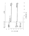
- FIG. 3A to 3C are graphs summarizing the film formation condition dependence of the drive voltage of each hole-only element 1000B.
- Each point in FIG. 3A corresponds to an element No. from left to right.
- the drive voltages of 4, 10, and 2 are represented.
- Each point in FIG. 3B is an element No. from left to right.
- the drive voltage of 13, 10, 1 is represented.
- each point in FIG. The drive voltages of 14, 2, and 8 are represented.
- the dependence of the driving voltage on the total pressure is at least in the range where the total pressure exceeds 2.7 Pa and 4.8 Pa or less under the conditions of the oxygen gas partial pressure of 50% and the input power of 500 W.
- FIG. 5 a clear reduction in drive voltage was confirmed. It was found by another experiment that this tendency continues at least until the total pressure is 7.0 Pa or less. Therefore, it can be said that the total pressure is desirably set in the range of more than 2.7 Pa and 7.0 Pa or less.
- the dependency of the driving voltage on the oxygen gas partial pressure is at least an oxygen gas partial pressure of 50% to 70% under the conditions of a total pressure of 2.7 Pa and an input power of 500 W.
- the driving voltage decreased with the increase of the oxygen gas partial pressure.
- the oxygen gas partial pressure is preferably 50% or more and the upper limit is preferably suppressed to about 70%.
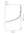
- the element No. The current density-applied voltage curves of 14, 1, and 7 are shown in FIG.
- the vertical axis represents current density (mA / cm 2 )
- the horizontal axis represents applied voltage (V).
- Element No. No. 14 satisfies all the desirable conditions of the total pressure, oxygen gas partial pressure, and input power described above. On the other hand, element No. 1 and 7 do not partially satisfy the above desirable conditions.
- the element No. No. 14 film forming conditions are film forming conditions A and element no. No. 1 film formation condition B, element No.
- the film formation condition 7 is referred to as film formation condition C.
- element no. 1 is HOD-B
- element no. 7 was also described as HOD-C.
- HOD-A As shown in FIG. 4, compared with HOD-B and HOD-C, HOD-A has the fastest rise in current density-applied voltage curve and a high current density at the lowest applied voltage. . That is, it is clear that HOD-A is superior in hole injection efficiency compared to HOD-B and HOD-C. Note that HOD-A is an element having the lowest drive voltage among the hole-only elements 1000B.
- the above is the verification regarding the hole injection efficiency of the hole injection layer 4 in the hole-only element 1000B.
- the hole-only element 1000B has the same configuration as the organic EL element 1000 of FIG. 1 except for the cathode. Accordingly, also in the organic EL element 1000, the dependency of the hole injection efficiency from the hole injection layer 4 to the buffer layer 6A on the film formation conditions is essentially the same as that of the hole only element 1000B. In order to confirm this, each organic EL element 1000 using the hole injection layer 4 under the deposition conditions A, B, and C was fabricated.
- each of the organic EL elements 1000 produced specifically has an anode 2 made of an ITO thin film having a thickness of 50 nm formed on a substrate 1 and further made of tungsten oxide having a thickness of 30 nm on the anode 2.
- Hole injection layer 4 buffer layer 6A made of TFB which is an amine organic polymer having a thickness of 20 nm
- light emitting layer 6B made of F8BT which is an organic polymer having a thickness of 70 nm
- barium having a thickness of 5 nm and aluminum having a thickness of 100 nm
- the cathode 8 made of the above was sequentially laminated. Note that the bank 5 is omitted because it is an evaluation device.
- FIG. 5 shows a current density-applied voltage curve representing the relationship between the applied voltage at this time and the current value flowing according to each voltage value when converted to a value per unit area of the element.
- the vertical axis represents current density (mA / cm 2 )
- the horizontal axis represents applied voltage (V).
- the organic EL element 1000 under film formation condition A is BPD-A
- the organic EL element 1000 under film formation condition B is BPD-B
- the organic EL element 1000 under film formation condition C is used.
- BPD-C the organic EL element 1000 under film formation condition
- BPD-A has the fastest rise in the current density-applied voltage curve compared to BPD-B and BPD-C, and a high current density is obtained at the lowest applied voltage. .
- This is the same tendency as HOD-A, HOD-B, and HOD-C, which are hole-only elements having the same film forming conditions.
- the emission intensity-current density curve showing the relationship of the emission intensity according to the change of the current density for each of the produced organic EL elements 1000 is shown in FIG.
- the vertical axis represents emission intensity (cd / A) and the horizontal axis represents current density (mA / cm 2 ). According to FIG. 6, it was confirmed that BPD-A has the highest emission intensity at least in the measured current density range.
- tungsten oxide constituting the hole injection layer 4 is a DC magnetron sputtering apparatus
- the target is metallic tungsten
- the substrate temperature is not controlled
- the gas in the chamber is argon gas and oxygen. It is composed of gas, the total pressure is more than 2.7 Pa and 7.0 Pa or less, the ratio of the oxygen gas partial pressure to the total pressure is 50% or more and 70% or less, and the input power density is 1 W / cm 2 or more.
- the hole injection efficiency from the hole injection layer 4 to the buffer layer 6A is good, thereby achieving excellent low voltage driving and high light emission. It was confirmed that efficiency was realized.
- the conditions of input electric power were again expressed by input electric power density based on Table 2.
- the input power is adjusted so that the input power density satisfies the above conditions according to the target size.
- the hole injection layer 4 made of tungsten oxide having excellent hole injection efficiency can be obtained. Note that the total pressure and oxygen partial pressure do not depend on the size of the apparatus or the target.
- the substrate temperature is not intentionally set in a sputtering apparatus arranged in a room temperature environment. Therefore, the substrate temperature is room temperature at least before film formation. However, the substrate temperature may increase by several tens of degrees Celsius during film formation.
- the organic EL element 1000 in which the hole injection layer 4 is formed under the deposition condition A is the organic EL element 1000 of the present embodiment, and has an occupied level near the Fermi surface described above. This will be discussed later.
- the tungsten oxide constituting the hole injection layer 4 of the organic EL element 1000 of the present embodiment has an occupied level near the Fermi surface.
- the occupied level in the vicinity of the Fermi surface is formed by adjusting the film forming conditions shown in the previous experiment. Details are described below.
- the sample for photoelectron spectroscopy measurement was produced on each film-forming condition.
- a tungsten oxide layer 80 (corresponding to the hole injection layer 4) having a thickness of 10 nm is formed on the conductive silicon substrate 70 by the reactive sputtering method.
- the sample 1A under the film formation condition A will be referred to as sample A
- the sample 1A under the film formation condition B as sample B
- the sample 1A under the film formation condition C as sample C.
- Samples A, B, and C were all deposited in a sputtering apparatus and then transferred into a glove box connected to the sputtering apparatus and filled with nitrogen gas, and kept in a state where they were not exposed to the atmosphere. . And it enclosed with the transfer vessel in the said glove box, and mounted
- UPS ultraviolet photoelectron spectroscopy
- the UPS spectrum reflects the state of the occupied level such as the valence band from the surface of the measurement object to a depth of several nm. Therefore, in this experiment, the state of the occupied level in the surface layer of the tungsten oxide layer 80 was observed using UPS.
- UPS measurement conditions are as follows. In Samples A, B, and C, since the conductive silicon substrate 70 was used, no charge-up occurred during measurement. The measurement point interval was 0.05 eV.
- FIG. 8 shows a UPS spectrum of the tungsten oxide layer 80 of Sample A.
- the origin of the binding energy on the horizontal axis is the Fermi surface of the substrate 70, and the left direction is the positive direction.
- each occupied level of the tungsten oxide layer 80 will be described with reference to FIG.
- the ratio of the number of tungsten atoms to oxygen atoms in samples A, B, and C is approximately 1: 3.
- This composition ratio was determined by X-ray photoelectron spectroscopy (XPS). Specifically, using the photoelectron spectrometer, as in the UPS measurement, the tungsten oxide layer 80 is subjected to XPS measurement without exposure to the atmosphere, and tungsten and oxygen at a depth of several nm from the surface of the tungsten oxide layer 80 are measured. The composition ratio was estimated. In Table 4, the film forming conditions for the tungsten oxide layer 80 are also shown.
- the tungsten oxide layer 80 has an atomic arrangement based on tungsten trioxide, that is, oxygen atoms are converted into tungsten atoms at least within a range of several nanometers from the surface.
- the basic structure has a distorted rutile structure (a structure in which octahedrons share an apex oxygen atom with each other) bonded in octahedral coordination. Therefore, the region (x) in FIG.
- the tungsten trioxide crystal or the amorphous of the crystal is disordered (however, the bond is not broken and the basic structure is maintained). It is an occupied level derived from the structure and is a region corresponding to a so-called valence band.
- this inventor measured the X-ray absorption fine structure (XAFS) of the tungsten oxide layer 80, and confirmed that the said basic structure was formed in any of the samples A, B, and C.
- XAFS X-ray absorption fine structure
- the region (y) in FIG. 8 corresponds to the band gap between the valence band and the conduction band, but as this UPS spectrum shows, this region is different from the valence band in tungsten oxide. It is known that there may be a number of occupied levels. This is a level derived from another structure different from the basic structure, and is a so-called inter-gap level (in-gap state or gap state).
- FIG. 9 shows UPS spectra in the region (y) of the tungsten oxide layers 80 in the samples A, B, and C.
- FIG. The intensity of the spectrum shown in FIG. 9 was normalized by the value of the peak top of the peak (ii) located 3 to 4 eV higher than the point (iii) in FIG. 9 also shows the point (iii) at the same horizontal axis position as the point (iii) in FIG.
- the horizontal axis is expressed as a relative value (relative binding energy) with respect to the point (iii), and the binding energy decreases from left to right (Fermi surface side).
- tungsten oxide having a structure that is raised (not necessarily a peak) in a region having a binding energy of about 1.8 to 3.6 eV lower than the point (iii) in the UPS spectrum is used as the hole injection layer.
- excellent hole injection efficiency can be exhibited in the organic EL element.
- a region having a binding energy lower by about 2.0 to 3.2 eV than the point (iii) is a region where the raised structure is relatively easy to confirm and the raised portion is relatively steep. It can be said that it is particularly important.
- the raised structure in the UPS spectrum is referred to as “a raised structure near the Fermi surface”.
- the occupied level corresponding to the raised structure in the vicinity of the Fermi surface is the aforementioned “occupied level in the vicinity of the Fermi surface”.
- the UPS spectrum shown in FIG. 9 was subjected to two-term smoothing (with a smoothing factor of 1) 11 times, and then subjected to differentiation by the central difference method. . This is to smooth the variation factors such as background noise during UPS measurement, to smooth the differential curve, and to clarify the following discussion.
- the differential value is 0 in the region (v) from the binding energy measurable by the photoelectron spectrometer to the point (iv).
- the differential value increases almost at the rate of increase toward the high binding energy side. It only increases gradually.
- the shapes of the differential curves of the samples B and C in the regions (v) and (vi) are almost similar to the UPS spectra of the samples B and C shown in FIG. Therefore, it can be said that the shape of the UPS spectrum and its differential curve in the regions (v) and (vi) of the samples B and C are exponential shapes.
- the tungsten oxide layer 80 of sample A shows a sharp rise from the vicinity of the point (iv) to the point (iii), and the shape of the differential curve in the regions (v) and (vi) is exponential.
- the shape of the curve is clearly different. It is confirmed that such a sample A has a raised structure in the vicinity of the Fermi surface, which begins to rise near the point (iv) in the spectrum before differentiation in FIG. 9 and is different from the exponential spectrum shape. it can.
- the characteristic of Sample A is that, in other words, the occupied level near the Fermi surface exists in a range approximately 1.8 to 3.6 eV lower than the lowest binding energy in the valence band. In the range of approximately 2.0 to 3.2 eV lower than the lowest binding energy, the corresponding raised structure near the Fermi surface can be clearly confirmed by the UPS spectrum.
- FIG. 12 is an XPS spectrum of the tungsten oxide layer 80 of Sample A after exposure to the atmosphere.
- the UPS spectrum (same as in FIG. 8) of the tungsten oxide layer 80 of Sample A was overwritten.
- XPS measurement conditions are the same as the UPS measurement conditions described above, except that the light source is Al K ⁇ rays.
- the point (iii) in the figure is the same horizontal axis position as in FIG. 8, and the horizontal axis is shown by the relative binding energy with respect to the point (iii) as in FIG. Further, the line corresponding to (i) of FIG. 8 in the XPS spectrum is indicated by (i) ′ in FIG.
- the raised structure in the vicinity of the Fermi surface in the tungsten oxide layer 80 of sample A is approximately 1.8 lower than the lowest binding energy in the valence band in the XPS spectrum as in the case of the UPS spectrum. Within the range of ⁇ 3.6 eV, the existence of a considerably large raised structure can be clearly confirmed. In another experiment, a raised structure in the vicinity of the Fermi surface was also confirmed by hard X-ray photoelectron spectroscopy.
- a sample 1A (FIG. 1A) formed by forming a tungsten oxide layer 80 on a conductive silicon substrate 70. 7) was used. This is merely a measure for preventing charge-up during measurement, and the structure of the organic EL element of the present invention is not limited to this configuration.
- the structure of the organic EL element 1000 shown in FIG. 1 (the structure in which the anode 2 made of ITO and the hole injection layer 4 made of tungsten oxide are sequentially formed on one surface of the substrate 1.
- the absolute value of the binding energy indicated by each occupied level of the hole injection layer 4 may differ from that of the tungsten oxide layer 80 of the sample 1A, but at least in the range from the band gap to the lowest binding energy in the valence band, a spectrum having the same shape as the sample 1A is obtained. ing.
- tungsten oxide a semi-occupied 5d orbital of a single tungsten atom having a lower binding energy than the bonding orbital between adjacent 5d orbitals of tungsten atoms or a structure similar thereto occupies near the Fermi surface. I think that it corresponds to a level.
- FIG. 13 is an energy diagram at the interface between the ⁇ -NPD layer and the tungsten oxide layer having an occupied level near the Fermi surface of the present invention.
- FIG. 13 first, in the tungsten oxide layer (corresponding to the hole injection layer), the lowest binding energy in the valence band (denoted as “upper end of valence band” in the figure) and the occupancy quasi near the Fermi surface.
- the binding energy at the rising position shown as “in-gap state upper end” in the figure.
- the upper end of the valence band corresponds to the point (iii) in FIG. 8
- the upper end of the in-gap state corresponds to the point (iv) in FIG.
- the thickness of the ⁇ -NPD layer when ⁇ -NPD (corresponding to a functional layer) is laminated on the tungsten oxide layer, the thickness of the ⁇ -NPD layer, the binding energy of the highest occupied orbit of ⁇ -NPD, and the vacuum level It also shows the relationship with the rank.
- the binding energy of the highest occupied orbit of ⁇ -NPD is the binding energy at the peak rising position of the highest occupied orbit in the UPS spectrum.
- the tungsten oxide layer formed on the ITO substrate is moved back and forth between the photoelectron spectrometer and the ultra-high vacuum deposition apparatus connected to the apparatus, and UPS measurement and ⁇ -NPD are performed.
- the energy diagram of FIG. 13 was obtained by repeating ultra-high vacuum deposition. Since no charge-up was confirmed during the UPS measurement, in FIG. 13, the binding energy on the vertical axis is expressed as an absolute value with the Fermi surface of the ITO substrate as the origin.
- FIG. 13 shows that the interface state connection is realized not by chance but by the interaction between tungsten oxide and ⁇ -NPD.
- the change in vacuum level (vacuum level shift) at the interface is that the electric double layer is formed at the interface with the tungsten oxide layer side negative and the ⁇ -NPD layer side positive based on the direction of the change.
- the magnitude of the vacuum level shift is as large as nearly 2 eV, it is appropriate to consider that the electric double layer is formed by an action similar to a chemical bond. That is, it should be considered that the interface state connection is realized by the interaction between tungsten oxide and ⁇ -NPD.
- the inventor of the present application infers the following mechanism as a specific interaction.
- the occupied level in the vicinity of the Fermi surface is derived from the 5d orbit of the tungsten atom as described above. This is hereinafter referred to as “the raised W5d trajectory”.
- the raised structure When the highest occupied orbit of the ⁇ -NPD molecule approaches the W5d orbit of the raised structure on the surface of the tungsten oxide layer, the raised structure is separated from the highest occupied orbit of the ⁇ -NPD molecule for mutual energy stabilization. Move to the W5d orbit. As a result, an electric double layer is formed at the interface, and vacuum level shift and interface level connection occur.
- the highest occupied orbitals of ⁇ -NPD molecules are distributed with the probability density biased toward the nitrogen atoms of the amine structure, and are composed mainly of unshared electron pairs of the nitrogen atoms. Many have been reported as a result of first-principles calculations. From this, it is presumed that electrons move from the unshared electron pair of the nitrogen atom of the amine structure to the W5d orbit of the raised structure at the interface between the tungsten oxide layer and the amine organic molecule layer.
- FIG. There is a report of interface state connection similar to the interface state connection between the tungsten oxide layer and the ⁇ -NPD layer shown in (3).
- the excellent hole injection efficiency of the hole injection layer of the organic EL element of the present invention can be explained by the above interface state connection. That is, an interface state connection occurs between a hole injection layer made of tungsten oxide having an occupied level near the Fermi surface and an adjacent functional layer, and the binding energy at the rising position of the occupied level near the Fermi surface The binding energy of the highest occupied orbit of the functional layer is almost equal. Hole injection occurs between the connected levels. Therefore, the hole injection barrier when injecting holes into the highest occupied orbit of the functional layer is almost nothing.
- the highest occupied orbitals of the organic molecules constituting the functional layer interact with the occupied levels near the Fermi surface of the tungsten oxide layer.
- Sites where the probability density of the highest occupied orbitals is high for example, nitrogen atoms of amine structures in amine-based organic molecules, indicated by “injection sites (y)” in the figure), oxygen defects in tungsten oxide layers, and similar structures ( (Indicated by “injection site (x)” in the figure) needs to approach (contact) to an interacting distance.
- the tungsten oxide layer having no raised structure near the Fermi surface such as the samples B and C described above, has the number density even if the implantation site (x) exists. In the UPS spectrum, it is so small that it does not reach the raised structure near the Fermi surface. Therefore, the possibility that the injection site (y) is in contact with the injection site (x) is very low. Since holes are injected where the injection site (x) and the injection site (y) are in contact, it can be seen that the efficiency of the samples B and C is extremely poor.
- the tungsten oxide layer having a raised structure near the Fermi surface such as the above-described sample A, has abundant injection sites (y). Therefore, it is highly possible that the injection site (y) is in contact with the injection site (x), and the hole injection efficiency is high.
- the organic EL device of the present invention has excellent hole injection efficiency.
- the hole injection layer made of tungsten oxide has a raised structure near the Fermi surface in its photoelectron spectroscopy spectrum. This means that oxygen defects and similar structures are present on the surface.
- the occupied level itself in the vicinity of the Fermi surface has the effect of connecting the interface state with the highest occupied orbital of the organic molecule by taking electrons from the organic molecule constituting the adjacent functional layer.
- the thickness of the hole injection layer is thinner than that immediately after forming the layer (hereinafter referred to as “film reduction”). I found.
- film reduction the thickness of the hole injection layer
- the inventors of the present application speculated that the decrease in the thickness of the hole injection layer occurred in the bank formation process.
- the following confirmation experiment was conducted.
- a layer made of tungsten oxide serving as a hole injection layer was first formed on a glass substrate by sputtering (the film formation conditions were the same as those for the hole-only device). Then, a resin material layer made of a predetermined resin material (“TFR” series manufactured by Tokyo Ohka Kogyo Co., Ltd.) is laminated on the hole injection layer based on a spin coating method (room temperature, 2500 rpm / 25 sec), and a baking process is performed. (100 ° C., 90 sec). Next, development processing (using TMAH 2.38% solution, developing time 60 sec) and cleaning processing (using pure water, cleaning time 60 sec) were performed. Thereafter, the resin material layer was peeled off. The arrangement of the resin material layer, the development process, and the cleaning process assume an actual bank formation process.
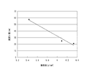
- FIG. 15 shows a graph showing the relationship between the film density and the film loss amount in Table 5.
- the tungsten oxide layer which is a hole injection layer, finally had a thickness of about 23 nm with respect to the film thickness immediately after film formation (80 nm). As a result, it was confirmed that the tungsten oxide layer having a thickness of about 57 nm actually disappeared due to film reduction (see Sample A having the best characteristics).
- the tungsten oxide layer has a lower film density as film characteristics such as light emission characteristics are better.
- the tungsten oxide layer has a structure derived from oxygen defects in the layer, so that the film density is reduced and good hole injection property is obtained. It can be assumed that driving can be realized.
- the inventors of the present application investigated the cause of the film loss of the tungsten oxide layer, and found that the tungsten oxide layer was dissolved and generated by the solvent used in the development process or the cleaning process. As described above, when the tungsten oxide layer has a structure derived from oxygen defects, the film density is lowered. This seems to be because a large number of minute crystal structures are formed in the layer. As a result of the formation of a large number of such fine crystal structures, the solvent (developer, cleaning solution, etc.) used in the film formation process when forming the bank is likely to enter the tungsten oxide layer, resulting in film reduction. It is thought to generate.
- the inventors of the present application dared to study this point and, for example, change the developing conditions (reducing the developer concentration from 2.38% to around 0.2%) or appropriately change the baking conditions. Thus, it was found that the amount of film loss of the tungsten oxide layer can be adjusted. Thereby, it is possible to control the film thickness of the tungsten oxide layer in consideration of film thickness reduction. Accordingly, the inventors of the present application have relied on the technology relating to the adjustment of the amount of film loss of the hole injection layer, and have further studied the trial manufacture of a realistic light emitting element, and have confirmed the following technical matters.
- a hole injection layer containing tungsten oxide was first formed on the anode.
- a bank material layer is laminated on the hole injection layer, and then the bank material layer is patterned into a predetermined shape having an opening for forming a functional layer (at this time, each process of exposure, development, and cleaning is performed) To do). Thereafter, a functional layer is formed at a position corresponding to the opening.
- a cathode was formed on the functional layer.
- the inventors of the present application have conceived a configuration in which a problem caused by the concentration of an electric field at the edge of such a recessed structure is prevented by the shape of the bank, as shown in the following embodiment.
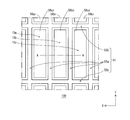
- FIG. 17 is a plan view showing a part of the organic EL display according to Embodiment 2 of the present invention.
- the organic EL display 100 is a top emission type in which organic EL elements 10a, 10b, and 10c (corresponding to the organic EL element 1000 of the first embodiment) having any of RGB light emitting layers are arranged in a matrix. This is an organic EL display. Each organic EL element functions as a sub-pixel, and a set of three organic EL elements of RGB functions as a pixel.
- a cross-shaped pixel bank 55 is employed, and the light emitting layers 6B6a1, 56b1, and 56c1 adjacent to each other in the X axis direction are separated by the bank elements 55a extending in the Y axis direction, and the light emitting layer is formed. 6B6a2, 56b2, and 56c2 are sectioned.
- the bank elements 55b extending in the X-axis direction separate the light emitting layers 6B6a1 and 56a2 adjacent in the Y-axis direction, the light emitting layers 6B6b1 and 56b2, and the light emitting layers 6B6c1 and 56c2.
- FIG. 18 is an end view schematically showing a partial cross section of the organic EL display according to the embodiment of the present invention, and shows a cross section taken along line AA of FIG.
- FIG. 19 is an enlarged end view of a portion B surrounded by an alternate long and short dash line in FIG.
- a hole injection layer 4 is disposed on the upper surface of the anode 2 via an ITO layer 3.
- the buffer layer 6A is omitted, and the electron injection layer 7 is disposed on the light emitting layer 6B, and the sealing layer 9 is disposed on the cathode 8.
- an anode 2 is formed in a matrix, and an ITO (indium tin oxide) layer 3 and a hole injection layer 4 are laminated on the anode 2 in this order.
- the ITO layer 3 is laminated only on the anode 2, whereas the hole injection layer 4 is formed not only on the anode 2 but over the entire upper surface of the substrate 1.
- the ITO layer 3 is interposed between the anode 2 and the hole injection layer 4 and has a function of improving the bonding property between the layers.
- a bank 5 is formed on the upper periphery of the anode 2 via a hole injection layer 4, and a light emitting layer 6 B is laminated in a region defined by the bank 5. Further, on the light emitting layer 6B, the electron injection layer 7, the cathode 8, and the sealing layer 9 are continuously connected to the organic EL elements 10a, 10b, and 10c adjacent to each other beyond the region defined by the bank 5. It is formed to do.
- the electron injection layer 7 has a function of transporting electrons injected from the cathode 8 to the light emitting layer 6B, and is preferably formed of, for example, barium, phthalocyanine, lithium fluoride, or a combination thereof.
- the cathode 8 has a single-layer structure here, and is formed of, for example, ITO, IZO (indium zinc oxide) or the like. In the case of a top emission type light emitting element, it is preferably formed of a light transmissive material.
- the sealing layer 9 has a function of preventing the light emitting layer 6B and the like from being exposed to moisture or air, and is made of, for example, a material such as SiN (silicon nitride) or SiON (silicon oxynitride). It is formed. In the case of a top emission type light emitting element, it is preferably formed of a light transmissive material.
- the hole injection layer 4 is the same as that of the first embodiment, and is composed of a tungsten oxide (WOx) layer formed under film formation conditions capable of obtaining good hole injection characteristics.
- WOx tungsten oxide
- the hole injection layer 4 extends laterally along the bottom surfaces 5 a and 5 b of the bank 5, and a recess 4 a is formed by recessing a part of the top surface. .
- a bottom surface 4b as an inner bottom surface portion of the recess 4a is depressed below the level 5c of the bank bottom surface 5a.
- the recess 4a includes a bottom surface 4b and a side surface 4d as an inner side surface continuous with the bottom surface 4b.
- the depth of the recess 4a is approximately 5 nm to 30 nm.
- the edge 4c of the recess is a convex corner portion formed by the region 4e that is not recessed on the upper surface of the hole injection layer 4 and the side surface 4d of the recess, and is covered with the covering portion 5d that is a part of the bank 5. Yes.
- the edge 4c of the recess protrudes with respect to the bottom surface 4b of the recess, if the edge 4c of the recess is not covered with the insulating coating 5d, electric field concentration occurs here, and the light emitting layer 6B is locally localized. As a result, current flows, and as a result, there arises a problem that the life of the product is shortened due to uneven brightness in the light emitting surface and local deterioration of the light emitting layer 6B.
- the edge 4c of the recess is covered with the insulating covering portion 5d, it is possible to suppress the occurrence of such a problem.
- the thickness of the covering portion 5d (the shortest distance from the edge 4c of the concave portion to the light emitting layer 6B) be 2 nm to 5 nm.
- the shape of the edge 4c of the recess is made polygonal or rounded as compared with the edge shape as shown in FIG. 19 as an example, so that electric field concentration can be further suppressed.
- the covering portion 5d reaches the bottom surface 4b of the recess 4a, and the side surface of the bank 5 is an upward slope from the point reaching the recess bottom surface 4b to the apex.
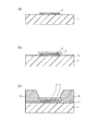
- FIG. 16 is an end view showing the manufacturing process of the organic EL display.
- FIG. 16A shows a state in which the anode 2, the ITO layer 3, the hole injection layer 4 and the bank 5 are formed on the TFT substrate 1.
- FIG. 16B shows a state where the light emitting layer 6B, the electron injection layer 7, the cathode 8 and the sealing layer 9 are further formed.
- the recess 4a is formed on the upper surface of the hole injection layer 4 in the process of forming the bank 5 (see FIG. 16A).
- the electric field is concentrated near the edge 4c of the recess during light emission.
- a current may flow locally in the light emitting layer 6B, and the generation of the local current may cause a problem of shortening the life due to luminance unevenness in the light emitting surface or local deterioration. is there.
- the present inventor has covered the edge of the recess formed in the charge injecting and transporting layer containing tungsten oxide with a part of the bank, so that the vicinity of the edge of the recess during light emission can be obtained. It was possible to conceive the technical feature of suppressing the concentration of electric charges and, as a result, suppressing the local current flow in the light emitting layer.
- ⁇ Method for manufacturing organic EL display> 20 to 22 are process diagrams illustrating a method for manufacturing an organic EL display according to an embodiment of the present invention.
- an Ag thin film is formed on a substrate 1 by sputtering, for example, and the Ag thin film is patterned by photolithography, for example, to form anodes 2 in a matrix.
- the Ag thin film may be formed by vacuum deposition or the like.
- an ITO thin film is formed by, for example, sputtering, and the ITO layer 3 is formed by patterning the ITO thin film by, for example, photolithography.
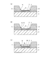
- a thin film 11 of WOx or MoxWyOz is formed by a technique such as vacuum deposition or sputtering using a composition containing WOx or MoxWyOz.
- a bank material layer 12 is formed on the thin film 11, and a part of the bank material layer 12 is removed to expose a part of the thin film 11.
- the bank material layer 12 can be formed, for example, by coating.
- the removal of the bank material layer 12 can be performed by forming a resist pattern on the bank material layer 12 and then performing etching.
- the resist pattern is removed after etching by, for example, an aqueous or non-aqueous release agent.
- etching residue is washed with pure water.
- WOx or MoxWyOz which is a material constituting the thin film 11, has a property of being easily dissolved in pure water, so that the exposed portion of the thin film 11 is eroded to form a concave structure as shown in FIG. The As a result, a hole injection layer 4 having a recess 4a is formed.
- heat treatment is performed to give a certain degree of fluidity to the remaining portion of the bank material layer 12, and the bank material is extended from the remaining portion to the edge 4c of the recess. As a result, the edge 4c of the recess is covered with the covering portion 5d.
- heat curing can be employed for the heat treatment. The temperature and time of the heat curing may be appropriately determined in consideration of the type of bank material, the required thickness of the covering portion 5d, and the like.
- the surface of the remaining portion of the bank material layer 12 is subjected to a liquid repellent treatment using, for example, fluorine plasma to form the bank 5.
- a composition ink (hereinafter simply referred to as “ink”) containing an organic EL material is dropped into the region defined by the bank 5 by, for example, an ink jet method. Is dried to form the light emitting layer 6B.
- the ink may be dropped by a dispenser method, a nozzle coating method, a spin coating method, intaglio printing, letterpress printing, or the like.
- a barium thin film that becomes the electron injection layer 7 is formed by, for example, vacuum deposition, and an ITO thin film that becomes the cathode 8 is formed by, for example, sputtering, as shown in FIG. 22B.
- the sealing layer 9 is further formed.
- the manufacturing method even if the recessed portion 4a is formed in the exposed portion of the hole injection layer 4 in the manufacturing process, the edge 4c of the recessed portion is covered with the covering portion 5d, and then the light emitting layer 6B is formed. It is possible to suppress the concentration of the electric field on the edge 4c of the recess.
- this invention is not limited to these embodiment.
- the following modifications can be considered.
- WOx or MoxWyOz is used as the material constituting the hole injection layer 4, but in general, metal oxides, nitrides, and oxynitrides are easily eroded by pure water. Therefore, even when a metal other than Mo (molybdenum) and W (tungsten) is used, the same effect can be obtained by applying this embodiment.
- the hole injection layer is eroded by pure water during cleaning to form a recess, but if the present invention is adopted, the recess may be formed for other reasons.
- the effect of suppressing the concentration of the electric field on the edge of the recess can be obtained.
- Other reasons include, for example, the case where the hole injection layer is eroded by an etching solution during etching or the case where the hole injection layer is eroded by a stripping agent during resist stripping.
- the hole injection layer is made of a material eroded by the liquid used when forming the bank, more specifically, the material eroded by the liquid used with a part of the hole injection layer exposed.
- the present invention is effective when consisting of: (3)
- the covering portion extending from the bank reaches the bottom surface 4b of the recess beyond the edge 4c of the recess, but the present invention only needs to cover the edge 4c of the recess.
- the cover 5d may not reach the bottom surface 4b of the recess.
- the bank material does not have to flow to the bottom of the recess, so that the heat treatment temperature and time can be reduced to a short time.
- the present invention uses mask patterning as another forming method. You can also (4) In FIG. 21A, the lower end of the slope of the bank material 12 and the edge 4c of the recess coincide, but this is not necessarily the case.
- a part of the non-recessed region 4e may be exposed due to the slope of the bank material 12 retreating. Even in this case, the bank material 12 may be appropriately heat-treated to cover the edge 4c of the recess with a part of the bank material (see FIG. 24B).
- a hole transport layer 13 may be formed on the hole injection layer 4, and these may be inserted as a charge injection transport layer.
- a recess is formed on the upper surface of the hole transport layer 13, and the edge of the recess formed in the hole transport layer is covered with the covering portion.
- the charge injection / transport layer may be composed of only the hole injection layer, and the hole injection layer and the hole transport layer constituting the functional layer may be interposed between the anode and the light emitting layer.
- a hole 4c is formed on the recess 4a of the hole injection layer 4 in a state where the edge 4c of the recess 4a of the hole injection layer 4 is covered by the cover 5d of the bank 5.
- the hole transport layer 13 may be formed by applying an ink containing a transport material
- the light emitting layer 6 may be formed by applying an ink containing a light emitting material on the hole transport layer 13.
- the hole transport layer is a layer having a thickness of about 10 nm to 20 nm and has a function of transporting holes injected from the hole injection layer into the organic light emitting layer.
- a hole transporting organic material is used as the hole transport layer.
- the hole transporting organic material is an organic substance having a property of transferring generated holes by intermolecular charge transfer reaction. This is sometimes called a p-type organic semiconductor.
- the hole transport layer may be a high molecular material or a low molecular material, but is formed by a wet printing method.
- a crosslinking agent so that it is difficult to elute into the organic light emitting layer.
- a copolymer containing a fluorene moiety and a triarylamine moiety or a low molecular weight triarylamine derivative can be used.
- the crosslinking agent dipentaerythritol hexaacrylate or the like can be used.
- the anode 2 is preferably formed of poly (3,4-ethylenedioxythiophene) doped with polystyrene sulfonic acid (PEDOT-PSS) or a derivative thereof (such as a copolymer).
- PEDOT-PSS polystyrene sulfonic acid
- the ITO layer 3 is formed thereon.
- the anode 2 is made of Al, the ITO layer 3 can be eliminated and the anode can have a single layer structure.
- an organic EL display is described as an example of a light-emitting device including a plurality of light-emitting elements, but the present invention is not limited to this and can be applied to a lighting device or the like. .
- a so-called pixel bank is used, but the present invention is not limited to this.
- a line bank (line-shaped bank) can be adopted.
- the line bank 65 is adopted, and the light emitting layers 6B6a, 66b, and 66c adjacent in the X-axis direction are divided.
- the driving method, the size and interval of the anode, etc. are appropriately set. By doing so, it is possible to emit light without affecting each other.
- the present invention is not limited to this and may be a bottom emission type.
- the electron injection layer is interposed between the light emitting layer and the cathode, but in addition to this, an electron transport layer may be interposed.
- an organic material is used as the bank material, but an inorganic material can also be used.
- the bank material layer can be formed by coating, for example, as in the case of using an organic material.
- the removal of the bank material layer can be performed by forming a resist pattern on the bank material layer and then performing etching using a predetermined etching solution (tetramethylammonium hydroxide oxide (TMAH) solution or the like).
- TMAH tetramethylammonium hydroxide oxide
- the resist pattern is removed after etching by, for example, an aqueous or non-aqueous release agent. Next, the etching residue is washed with pure water.
- the “occupied level” referred to in this specification includes an electron level by an electron orbit occupied by at least one electron, that is, a so-called semi-occupied orbital level.
- the organic EL element of the present invention is not limited to the configuration used alone.
- An organic EL panel can also be configured by integrating a plurality of organic EL elements as pixels on a substrate.
- Such an organic EL display can be implemented by appropriately setting the film thickness of each layer in each element.
- the organic EL device of the present invention can be used for display devices for mobile phones, display devices for televisions, various light sources, and the like. In any application, it can be applied as an organic EL element that is driven at a low voltage in a wide luminance range from low luminance to high luminance such as a light source. With such high performance, it can be widely used as various display devices for home or public facilities, or for business use, television devices, displays for portable electronic devices, illumination light sources, and the like.
Landscapes
- Physics & Mathematics (AREA)
- Optics & Photonics (AREA)
- Electroluminescent Light Sources (AREA)
Abstract
Priority Applications (4)
| Application Number | Priority Date | Filing Date | Title |
|---|---|---|---|
| CN201080068374.7A CN103053040B (zh) | 2010-08-06 | 2010-08-06 | 有机el元件 |
| JP2012527474A JP5677434B2 (ja) | 2010-08-06 | 2010-08-06 | 有機el素子 |
| PCT/JP2010/004987 WO2012017497A1 (fr) | 2010-08-06 | 2010-08-06 | Elément el organique |
| US13/739,363 US8999832B2 (en) | 2010-08-06 | 2013-01-11 | Organic EL element |
Applications Claiming Priority (1)
| Application Number | Priority Date | Filing Date | Title |
|---|---|---|---|
| PCT/JP2010/004987 WO2012017497A1 (fr) | 2010-08-06 | 2010-08-06 | Elément el organique |
Related Child Applications (1)
| Application Number | Title | Priority Date | Filing Date |
|---|---|---|---|
| US13/739,363 Continuation US8999832B2 (en) | 2010-08-06 | 2013-01-11 | Organic EL element |
Publications (1)
| Publication Number | Publication Date |
|---|---|
| WO2012017497A1 true WO2012017497A1 (fr) | 2012-02-09 |
Family
ID=45559030
Family Applications (1)
| Application Number | Title | Priority Date | Filing Date |
|---|---|---|---|
| PCT/JP2010/004987 Ceased WO2012017497A1 (fr) | 2010-08-06 | 2010-08-06 | Elément el organique |
Country Status (4)
| Country | Link |
|---|---|
| US (1) | US8999832B2 (fr) |
| JP (1) | JP5677434B2 (fr) |
| CN (1) | CN103053040B (fr) |
| WO (1) | WO2012017497A1 (fr) |
Families Citing this family (12)
| Publication number | Priority date | Publication date | Assignee | Title |
|---|---|---|---|---|
| EP2398085B1 (fr) | 2009-02-10 | 2018-06-27 | Joled Inc. | Elément électroluminescent, dispositif d'affichage et procédé de fabrication d'un élément électroluminescent |
| WO2012017503A1 (fr) | 2010-08-06 | 2012-02-09 | パナソニック株式会社 | Élément électroluminescent organique |
| JP5677432B2 (ja) * | 2010-08-06 | 2015-02-25 | パナソニック株式会社 | 有機el素子、表示装置および発光装置 |
| WO2012017502A1 (fr) | 2010-08-06 | 2012-02-09 | パナソニック株式会社 | Élément électroluminescent organique et son procédé de fabrication |
| WO2012017485A1 (fr) | 2010-08-06 | 2012-02-09 | パナソニック株式会社 | Élément électroluminescent organique, dispositif d'affichage et dispositif électroluminescent |
| JP5543600B2 (ja) | 2010-08-06 | 2014-07-09 | パナソニック株式会社 | 発光素子、発光素子を備えた発光装置および発光素子の製造方法 |
| JP5861210B2 (ja) | 2011-07-15 | 2016-02-16 | 株式会社Joled | 有機発光素子 |
| US9065069B2 (en) | 2011-07-15 | 2015-06-23 | Joled Inc. | Method for producing organic light-emitting element |
| JP5793569B2 (ja) | 2011-07-15 | 2015-10-14 | 株式会社Joled | 有機発光素子の製造方法 |
| JP6387547B2 (ja) | 2012-03-02 | 2018-09-12 | 株式会社Joled | 有機el素子とその製造方法、および金属酸化物膜の成膜方法 |
| WO2013179355A1 (fr) * | 2012-05-31 | 2013-12-05 | パナソニック株式会社 | Élément électroluminescent, transistor et cloison |
| KR102763305B1 (ko) * | 2019-11-26 | 2025-02-05 | 삼성디스플레이 주식회사 | 표시 장치 |
Citations (6)
| Publication number | Priority date | Publication date | Assignee | Title |
|---|---|---|---|---|
| JP2009218156A (ja) * | 2008-03-12 | 2009-09-24 | Casio Comput Co Ltd | Elパネル及びelパネルの製造方法 |
| JP2010010670A (ja) * | 2008-05-28 | 2010-01-14 | Panasonic Corp | 発光装置及びその製造方法 |
| JP2010033972A (ja) * | 2008-07-30 | 2010-02-12 | Sumitomo Chemical Co Ltd | 有機エレクトロルミネッセンス素子およびその製造方法 |
| JP2010050107A (ja) * | 2008-02-28 | 2010-03-04 | Panasonic Corp | 有機elディスプレイパネル |
| WO2010032444A1 (fr) * | 2008-09-19 | 2010-03-25 | パナソニック株式会社 | Élément électroluminescent organique et son procédé de fabrication |
| JP2010103374A (ja) * | 2008-10-24 | 2010-05-06 | Panasonic Corp | 有機エレクトロルミネッセンス素子及びその製造方法 |
Family Cites Families (116)
| Publication number | Priority date | Publication date | Assignee | Title |
|---|---|---|---|---|
| US5443922A (en) | 1991-11-07 | 1995-08-22 | Konica Corporation | Organic thin film electroluminescence element |
| JPH05163488A (ja) | 1991-12-17 | 1993-06-29 | Konica Corp | 有機薄膜エレクトロルミネッセンス素子 |
| US5294869A (en) | 1991-12-30 | 1994-03-15 | Eastman Kodak Company | Organic electroluminescent multicolor image display device |
| US5688551A (en) | 1995-11-13 | 1997-11-18 | Eastman Kodak Company | Method of forming an organic electroluminescent display panel |
| JPH10162959A (ja) | 1996-11-29 | 1998-06-19 | Idemitsu Kosan Co Ltd | 有機エレクトロルミネッセンス素子 |
| DE69729394T2 (de) | 1996-11-29 | 2005-06-02 | Idemitsu Kosan Co. Ltd. | Organische elektrolumineszente Vorrichtung |
| JP3782245B2 (ja) | 1998-10-28 | 2006-06-07 | Tdk株式会社 | 有機el表示装置の製造装置及び製造方法 |
| US6309801B1 (en) | 1998-11-18 | 2001-10-30 | U.S. Philips Corporation | Method of manufacturing an electronic device comprising two layers of organic-containing material |
| JP4198253B2 (ja) | 1999-02-02 | 2008-12-17 | 出光興産株式会社 | 有機エレクトロルミネッセンス素子およびその製造方法 |
| US7153592B2 (en) | 2000-08-31 | 2006-12-26 | Fujitsu Limited | Organic EL element and method of manufacturing the same, organic EL display device using the element, organic EL material, and surface emission device and liquid crystal display device using the material |
| JP2002075661A (ja) | 2000-08-31 | 2002-03-15 | Fujitsu Ltd | 有機el素子及び有機el表示装置 |
| TWI257496B (en) | 2001-04-20 | 2006-07-01 | Toshiba Corp | Display device and method of manufacturing the same |
| JP2002318556A (ja) | 2001-04-20 | 2002-10-31 | Toshiba Corp | アクティブマトリクス型平面表示装置およびその製造方法 |
| US8058797B2 (en) | 2001-05-18 | 2011-11-15 | Cambridge University Technical Services Limited | Electroluminescent device |
| JP2003007460A (ja) | 2001-06-22 | 2003-01-10 | Sony Corp | 表示装置の製造方法および表示装置 |
| JP3823916B2 (ja) | 2001-12-18 | 2006-09-20 | セイコーエプソン株式会社 | 表示装置及び電子機器並びに表示装置の製造方法 |
| US6815723B2 (en) | 2001-12-28 | 2004-11-09 | Semiconductor Energy Laboratory Co., Ltd. | Light emitting device, method of manufacturing the same, and manufacturing apparatus therefor |
| JP2003264083A (ja) | 2002-03-08 | 2003-09-19 | Sharp Corp | 有機led素子とその製造方法 |
| US7086917B2 (en) | 2002-08-12 | 2006-08-08 | National Research Council Of Canada | Photoresist mask/smoothing layer ensuring the field homogeneity and better step-coverage in OLED displays |
| JP4165173B2 (ja) | 2002-10-15 | 2008-10-15 | 株式会社デンソー | 有機el素子の製造方法 |
| JP2004228355A (ja) | 2003-01-23 | 2004-08-12 | Seiko Epson Corp | 絶縁膜基板の製造方法、絶縁膜基板の製造装置及び絶縁膜基板並びに電気光学装置の製造方法及び電気光学装置 |
| JP2004234901A (ja) | 2003-01-28 | 2004-08-19 | Seiko Epson Corp | ディスプレイ基板、有機el表示装置、ディスプレイ基板の製造方法および電子機器 |
| EP1629544B1 (fr) | 2003-05-12 | 2008-11-19 | Cambridge Enterprise Limited | Transistor polymere |
| ATE401672T1 (de) | 2003-05-12 | 2008-08-15 | Cambridge Entpr Ltd | Herstellung einer polymeren vorrichtung |
| JP2005012173A (ja) | 2003-05-28 | 2005-01-13 | Seiko Epson Corp | 膜パターン形成方法、デバイス及びデバイスの製造方法、電気光学装置、並びに電子機器 |
| JP2004363170A (ja) | 2003-06-02 | 2004-12-24 | Seiko Epson Corp | 導電パターンの形成方法、電気光学装置、電気光学装置の製造方法および電子機器 |
| US7492090B2 (en) | 2003-09-19 | 2009-02-17 | Semiconductor Energy Laboratory Co., Ltd. | Display device and method for manufacturing the same |
| US7230374B2 (en) | 2003-09-22 | 2007-06-12 | Samsung Sdi Co., Ltd. | Full color organic light-emitting device having color modulation layer |
| US20060139342A1 (en) | 2004-12-29 | 2006-06-29 | Gang Yu | Electronic devices and processes for forming electronic devices |
| KR20060110323A (ko) | 2003-12-16 | 2006-10-24 | 마츠시타 덴끼 산교 가부시키가이샤 | 유기 전기발광 소자 및 그 제조 방법 |
| JP2005203339A (ja) | 2003-12-16 | 2005-07-28 | Matsushita Electric Ind Co Ltd | 有機エレクトロルミネッセント素子およびその製造方法 |
| US20090160325A1 (en) | 2003-12-16 | 2009-06-25 | Panasonic Corporation | Organic electroluminescent device and method for manufacturing the same |
| JP2005203340A (ja) | 2003-12-16 | 2005-07-28 | Matsushita Electric Ind Co Ltd | 有機エレクトロルミネッセント素子 |
| JP4857521B2 (ja) | 2004-01-09 | 2012-01-18 | セイコーエプソン株式会社 | 電気光学装置の製造方法、電気光学装置、及び電子機器 |
| JP4002949B2 (ja) | 2004-03-17 | 2007-11-07 | 独立行政法人科学技術振興機構 | 両面発光有機elパネル |
| JP2005268099A (ja) | 2004-03-19 | 2005-09-29 | Mitsubishi Electric Corp | 有機el表示パネル、有機el表示装置、および有機el表示パネルの製造方法 |
| JP4645064B2 (ja) | 2004-05-19 | 2011-03-09 | セイコーエプソン株式会社 | 電気光学装置の製造方法 |
| US7541099B2 (en) | 2004-05-21 | 2009-06-02 | Semiconductor Energy Laboratory Co., Ltd. | Anthracene derivative and light emitting element and light emitting device using the same |
| JP4161956B2 (ja) | 2004-05-27 | 2008-10-08 | セイコーエプソン株式会社 | カラーフィルタ基板の製造方法、電気光学装置の製造方法、電気光学装置、電子機器 |
| CN100490213C (zh) * | 2004-05-27 | 2009-05-20 | 精工爱普生株式会社 | 滤色片基板的制造方法、电光学装置及其制造方法、电子设备 |
| US7211456B2 (en) | 2004-07-09 | 2007-05-01 | Au Optronics Corporation | Method for electro-luminescent display fabrication |
| JP2006185869A (ja) | 2004-12-28 | 2006-07-13 | Asahi Glass Co Ltd | 有機電界発光素子及びその製造方法 |
| DE102005007540A1 (de) | 2005-02-18 | 2006-08-31 | Robert Bosch Gmbh | Mikromechanischer Membransensor mit Doppelmembran |
| JP2006253443A (ja) | 2005-03-11 | 2006-09-21 | Seiko Epson Corp | 有機el装置、その製造方法および電子機器 |
| JP2006294261A (ja) | 2005-04-05 | 2006-10-26 | Fuji Electric Holdings Co Ltd | 有機el発光素子およびその製造方法 |
| TWI307612B (en) | 2005-04-27 | 2009-03-11 | Sony Corp | Transfer method and transfer apparatus |
| JP2006344459A (ja) | 2005-06-08 | 2006-12-21 | Sony Corp | 転写方法および転写装置 |
| JP2007073499A (ja) | 2005-08-08 | 2007-03-22 | Semiconductor Energy Lab Co Ltd | 発光装置およびその作製方法 |
| US7994711B2 (en) | 2005-08-08 | 2011-08-09 | Semiconductor Energy Laboratory Co., Ltd. | Light emitting device and manufacturing method thereof |
| US7635858B2 (en) | 2005-08-10 | 2009-12-22 | Au Optronics Corporation | Organic light-emitting device with improved layer conductivity distribution |
| GB0517195D0 (en) | 2005-08-23 | 2005-09-28 | Cambridge Display Tech Ltd | Molecular electronic device structures and fabrication methods |
| JP4106076B2 (ja) | 2005-09-29 | 2008-06-25 | 松下電器産業株式会社 | 有機elディスプレイおよびその製造方法 |
| JP2007095606A (ja) | 2005-09-30 | 2007-04-12 | Seiko Epson Corp | 有機el装置、その製造方法、及び電子機器 |
| JP2007150258A (ja) | 2005-10-27 | 2007-06-14 | Seiko Epson Corp | パターン形成方法、膜構造体、電気光学装置及び電子機器 |
| JP4318689B2 (ja) | 2005-12-09 | 2009-08-26 | 出光興産株式会社 | n型無機半導体、n型無機半導体薄膜及びその製造方法 |
| JP5256605B2 (ja) * | 2006-01-18 | 2013-08-07 | 凸版印刷株式会社 | 有機エレクトロルミネッセンス素子の製造方法 |
| JP2007214066A (ja) | 2006-02-13 | 2007-08-23 | Seiko Epson Corp | 有機エレクトロルミネセンス装置の製造方法 |
| US20070241665A1 (en) | 2006-04-12 | 2007-10-18 | Matsushita Electric Industrial Co., Ltd. | Organic electroluminescent element, and manufacturing method thereof, as well as display device and exposure apparatus using the same |
| JP2007288074A (ja) | 2006-04-19 | 2007-11-01 | Matsushita Electric Ind Co Ltd | 有機エレクトロルミネッセント素子およびその製造方法 |
| JP2007287353A (ja) | 2006-04-12 | 2007-11-01 | Matsushita Electric Ind Co Ltd | 有機エレクトロルミネッセント素子の製造方法およびそれを用いて作成された有機エレクトロルミネッセント素子 |
| JP2007288071A (ja) | 2006-04-19 | 2007-11-01 | Matsushita Electric Ind Co Ltd | 有機エレクトロルミネッセント素子およびその製造方法、それを用いた表示装置、露光装置 |
| US20070290604A1 (en) | 2006-06-16 | 2007-12-20 | Matsushita Electric Industrial Co., Ltd. | Organic electroluminescent device and method of producing the same |
| JP2008041747A (ja) | 2006-08-02 | 2008-02-21 | Matsushita Electric Ind Co Ltd | 有機エレクトロルミネッセント発光装置およびその製造方法 |
| JP4915650B2 (ja) | 2006-08-25 | 2012-04-11 | パナソニック株式会社 | 有機エレクトロルミネッセンス素子 |
| JP2008091072A (ja) | 2006-09-29 | 2008-04-17 | Seiko Epson Corp | 電気光学装置、およびその製造方法 |
| JP2008108530A (ja) | 2006-10-25 | 2008-05-08 | Hitachi Displays Ltd | 有機el表示装置 |
| JP4915913B2 (ja) | 2006-11-13 | 2012-04-11 | パナソニック株式会社 | 有機エレクトロルミネッセンス素子 |
| JP2008140724A (ja) | 2006-12-05 | 2008-06-19 | Toppan Printing Co Ltd | 有機el素子の製造方法および有機el素子 |
| WO2008075615A1 (fr) | 2006-12-21 | 2008-06-26 | Semiconductor Energy Laboratory Co., Ltd. | Élément et dispositif électroluminescents |
| JP4998710B2 (ja) | 2007-03-06 | 2012-08-15 | カシオ計算機株式会社 | 表示装置の製造方法 |
| JP5326289B2 (ja) | 2007-03-23 | 2013-10-30 | 凸版印刷株式会社 | 有機el素子およびそれを備えた表示装置 |
| US8471461B2 (en) | 2007-03-29 | 2013-06-25 | Dai Nippon Printing Co., Ltd. | Organic electroluminescent device and method for producing the same |
| JP2009004347A (ja) | 2007-05-18 | 2009-01-08 | Toppan Printing Co Ltd | 有機el表示素子の製造方法及び有機el表示素子 |
| KR100919352B1 (ko) | 2007-05-30 | 2009-09-25 | 파나소닉 주식회사 | 유기 el 디스플레이 패널 및 그 제조 방법 |
| JP4280301B2 (ja) | 2007-05-31 | 2009-06-17 | パナソニック株式会社 | 有機el素子、およびその製造方法 |
| US20080312437A1 (en) * | 2007-06-04 | 2008-12-18 | Semiconductor Energy Labratory Co., Ltd. | Organometallic Complex, and Light-Emitting Element, Light-Emitting Device, and Electronic Device Using the Organometallic Complex |
| US8628986B2 (en) | 2007-07-31 | 2014-01-14 | Sumitomo Chemical Company, Limited | Organic electroluminescent element and method for manufacturing the same |
| JP5001745B2 (ja) | 2007-08-10 | 2012-08-15 | 住友化学株式会社 | 有機エレクトロルミネッセンス素子及び製造方法 |
| JP2009048960A (ja) | 2007-08-23 | 2009-03-05 | Canon Inc | 電極洗浄処理方法 |
| JP2009058897A (ja) | 2007-09-03 | 2009-03-19 | Hitachi Displays Ltd | 表示装置 |
| US8083956B2 (en) | 2007-10-11 | 2011-12-27 | Semiconductor Energy Laboratory Co., Ltd. | Display device and method for manufacturing display device |
| JP2009135053A (ja) | 2007-11-30 | 2009-06-18 | Sumitomo Chemical Co Ltd | 電子デバイス、表示装置および電子デバイスの製造方法 |
| WO2009075075A1 (fr) | 2007-12-10 | 2009-06-18 | Panasonic Corporation | Dispositif électroluminescent organique, panneau d'affichage électroluminescent, procédé de fabrication du dispositif électroluminescent organique et procédé de fabrication du panneau d'affichage électroluminescent |
| JP4439589B2 (ja) | 2007-12-28 | 2010-03-24 | パナソニック株式会社 | 有機elデバイスおよび有機elディスプレイパネル、ならびにそれらの製造方法 |
| JP5267246B2 (ja) | 2008-03-26 | 2013-08-21 | 凸版印刷株式会社 | 有機エレクトロルミネッセンス素子及びその製造方法並びに有機エレクトロルミネッセンス表示装置 |
| JP2009239180A (ja) | 2008-03-28 | 2009-10-15 | Sumitomo Chemical Co Ltd | 有機エレクトロルミネッセンス素子 |
| KR100999739B1 (ko) * | 2008-04-02 | 2010-12-08 | 엘지이노텍 주식회사 | 발광소자 및 그 제조방법 |
| KR101509283B1 (ko) | 2008-04-28 | 2015-04-06 | 다이니폰 인사츠 가부시키가이샤 | 정공 주입 수송층을 갖는 디바이스, 및 그 제조 방법, 및 정공 주입 수송층 형성용 잉크 |
| JP4931858B2 (ja) | 2008-05-13 | 2012-05-16 | パナソニック株式会社 | 有機エレクトロルミネッセント素子の製造方法 |
| JP4678421B2 (ja) | 2008-05-16 | 2011-04-27 | ソニー株式会社 | 表示装置 |
| JP2008241238A (ja) | 2008-05-28 | 2008-10-09 | Mitsubishi Electric Corp | 冷凍空調装置及び冷凍空調装置の制御方法 |
| KR100984574B1 (ko) * | 2008-06-06 | 2010-09-30 | 파나소닉 주식회사 | 유기 el 디스플레이 패널 및 그 제조 방법 |
| JP2010021138A (ja) | 2008-06-09 | 2010-01-28 | Panasonic Corp | 有機エレクトロルミネッセント装置およびその製造方法 |
| GB0811199D0 (en) * | 2008-06-18 | 2008-07-23 | Cambridge Entpr Ltd | Electro-optic diode devices |
| JP4697265B2 (ja) | 2008-06-24 | 2011-06-08 | カシオ計算機株式会社 | 発光装置の製造方法 |
| US20090315027A1 (en) | 2008-06-24 | 2009-12-24 | Casio Computer Co., Ltd. | Light emitting device and manufacturing method of light emitting device |
| JP2011040167A (ja) | 2008-11-12 | 2011-02-24 | Panasonic Corp | 表示装置およびその製造方法 |
| JP2010123716A (ja) | 2008-11-19 | 2010-06-03 | Fujifilm Corp | 有機電界発光素子 |
| JP4856753B2 (ja) | 2008-12-10 | 2012-01-18 | パナソニック株式会社 | 光学素子および光学素子を具備する表示装置の製造方法 |
| KR101251725B1 (ko) | 2008-12-18 | 2013-04-05 | 파나소닉 주식회사 | 유기 일렉트로 루미네슨스 표시 장치 및 그 제조 방법 |
| JP2010153127A (ja) | 2008-12-24 | 2010-07-08 | Sony Corp | 表示装置 |
| JP2010161185A (ja) | 2009-01-08 | 2010-07-22 | Ulvac Japan Ltd | 有機el表示装置、有機el表示装置の製造方法 |
| EP2398085B1 (fr) | 2009-02-10 | 2018-06-27 | Joled Inc. | Elément électroluminescent, dispositif d'affichage et procédé de fabrication d'un élément électroluminescent |
| EP2398084B1 (fr) | 2009-02-10 | 2018-06-06 | Joled Inc. | Elément électroluminescent, dispositif électroluminescent comprenant l'élément électroluminescent et procédé de fabrication de l'élément électroluminescent |
| WO2011013523A1 (fr) | 2009-07-31 | 2011-02-03 | Semiconductor Energy Laboratory Co., Ltd. | Dispositif semi-conducteur et procédé de fabrication de celui-ci |
| JP5437736B2 (ja) | 2009-08-19 | 2014-03-12 | パナソニック株式会社 | 有機el素子 |
| KR101218844B1 (ko) | 2009-08-31 | 2013-01-21 | 파나소닉 주식회사 | 발광 소자와 그 제조 방법, 및 발광 장치 |
| KR101539479B1 (ko) | 2009-12-22 | 2015-07-24 | 가부시키가이샤 제이올레드 | 표시 장치와 그 제조 방법 |
| JP5574113B2 (ja) | 2009-12-22 | 2014-08-20 | パナソニック株式会社 | 表示装置とその製造方法 |
| KR101643009B1 (ko) | 2009-12-22 | 2016-07-27 | 가부시키가이샤 제이올레드 | 표시 장치와 그 제조 방법 |
| CN102334384B (zh) | 2010-02-22 | 2015-01-28 | 松下电器产业株式会社 | 发光装置及其制造方法 |
| CN102473847B (zh) | 2010-06-24 | 2015-01-14 | 松下电器产业株式会社 | 有机el元件、显示装置以及发光装置 |
| WO2012017495A1 (fr) | 2010-08-06 | 2012-02-09 | パナソニック株式会社 | Elément el organique et procédé de fabrication associé |
| WO2012017503A1 (fr) | 2010-08-06 | 2012-02-09 | パナソニック株式会社 | Élément électroluminescent organique |
| WO2012017502A1 (fr) | 2010-08-06 | 2012-02-09 | パナソニック株式会社 | Élément électroluminescent organique et son procédé de fabrication |
| KR101707254B1 (ko) | 2010-11-29 | 2017-02-15 | 가부시키가이샤 제이올레드 | 유기 발광 소자의 제조 방법, 유기 발광 소자, 발광 장치, 표시 패널, 및 표시 장치 |
-
2010
- 2010-08-06 WO PCT/JP2010/004987 patent/WO2012017497A1/fr not_active Ceased
- 2010-08-06 CN CN201080068374.7A patent/CN103053040B/zh active Active
- 2010-08-06 JP JP2012527474A patent/JP5677434B2/ja not_active Expired - Fee Related
-
2013
- 2013-01-11 US US13/739,363 patent/US8999832B2/en not_active Expired - Fee Related
Patent Citations (6)
| Publication number | Priority date | Publication date | Assignee | Title |
|---|---|---|---|---|
| JP2010050107A (ja) * | 2008-02-28 | 2010-03-04 | Panasonic Corp | 有機elディスプレイパネル |
| JP2009218156A (ja) * | 2008-03-12 | 2009-09-24 | Casio Comput Co Ltd | Elパネル及びelパネルの製造方法 |
| JP2010010670A (ja) * | 2008-05-28 | 2010-01-14 | Panasonic Corp | 発光装置及びその製造方法 |
| JP2010033972A (ja) * | 2008-07-30 | 2010-02-12 | Sumitomo Chemical Co Ltd | 有機エレクトロルミネッセンス素子およびその製造方法 |
| WO2010032444A1 (fr) * | 2008-09-19 | 2010-03-25 | パナソニック株式会社 | Élément électroluminescent organique et son procédé de fabrication |
| JP2010103374A (ja) * | 2008-10-24 | 2010-05-06 | Panasonic Corp | 有機エレクトロルミネッセンス素子及びその製造方法 |
Non-Patent Citations (3)
| Title |
|---|
| KANAME KANAI ET AL.: "Electronic structure of anode interface with molybdenum oxide buffer layer", ORGANIC ELECTRONICS, vol. 11, no. 2, February 2010 (2010-02-01), pages 188 - 194, XP026836239 * |
| KENJI KOIZUMI ET AL.: "a-NPD/Mo03 Kaimen ni Okeru Denshi Kozo", 2009 NEN SHUNKI DAI 56 KAI EXTENDED ABSTRACTS, JAPAN SOCIETY OF APPLIED PHYSICS AND RELATED SOCIETIES, vol. 3, 30 March 2009 (2009-03-30), pages 1279 * |
| MIN JUNG SON ET AL.: "Interface electronic structures of organic light-emitting diodes with W03 interlayer: A study by photoelectron spectroscopy", ORGANIC ELECTRINICS, vol. 10, no. 4, 2009, pages 637 - 642, XP026119395, DOI: doi:10.1016/j.orgel.2009.02.017 * |
Also Published As
| Publication number | Publication date |
|---|---|
| JP5677434B2 (ja) | 2015-02-25 |
| CN103053040B (zh) | 2015-09-02 |
| CN103053040A (zh) | 2013-04-17 |
| US8999832B2 (en) | 2015-04-07 |
| US20130126841A1 (en) | 2013-05-23 |
| JPWO2012017497A1 (ja) | 2013-09-19 |
Similar Documents
| Publication | Publication Date | Title |
|---|---|---|
| JP5677437B2 (ja) | 有機el素子 | |
| JP5677434B2 (ja) | 有機el素子 | |
| JP5437736B2 (ja) | 有機el素子 | |
| JP5884224B2 (ja) | 有機el表示パネルおよび有機el表示装置 | |
| JP5612691B2 (ja) | 有機el素子およびその製造方法 | |
| JP5677436B2 (ja) | 有機el素子 | |
| JP5676652B2 (ja) | 有機el素子 | |
| WO2012017502A1 (fr) | Élément électroluminescent organique et son procédé de fabrication | |
| KR20130096773A (ko) | 유기 발광 소자의 제조 방법, 유기 발광 소자, 발광 장치, 표시 패널, 및 표시 장치 | |
| WO2012017501A1 (fr) | Élément électroluminescent organique et son procédé de fabrication | |
| JP5861210B2 (ja) | 有機発光素子 | |
| JP5793569B2 (ja) | 有機発光素子の製造方法 | |
| JP6387547B2 (ja) | 有機el素子とその製造方法、および金属酸化物膜の成膜方法 | |
| JP5793570B2 (ja) | 有機発光素子の製造方法 |
Legal Events
| Date | Code | Title | Description |
|---|---|---|---|
| WWE | Wipo information: entry into national phase |
Ref document number: 201080068374.7 Country of ref document: CN |
|
| 121 | Ep: the epo has been informed by wipo that ep was designated in this application |
Ref document number: 10773523 Country of ref document: EP Kind code of ref document: A1 |
|
| WWE | Wipo information: entry into national phase |
Ref document number: 2012527474 Country of ref document: JP |
|
| NENP | Non-entry into the national phase |
Ref country code: DE |
|
| 122 | Ep: pct application non-entry in european phase |
Ref document number: 10773523 Country of ref document: EP Kind code of ref document: A1 |