WO2012017496A1 - Dispositif émetteur de lumière, appareil émettant de la lumière équipé dudit dispositif, et procédé de fabrication d'un dispositif émetteur de lumière - Google Patents
Dispositif émetteur de lumière, appareil émettant de la lumière équipé dudit dispositif, et procédé de fabrication d'un dispositif émetteur de lumière Download PDFInfo
- Publication number
- WO2012017496A1 WO2012017496A1 PCT/JP2010/004986 JP2010004986W WO2012017496A1 WO 2012017496 A1 WO2012017496 A1 WO 2012017496A1 JP 2010004986 W JP2010004986 W JP 2010004986W WO 2012017496 A1 WO2012017496 A1 WO 2012017496A1
- Authority
- WO
- WIPO (PCT)
- Prior art keywords
- light emitting
- layer
- bank
- electrode
- emitting device
- Prior art date
- Legal status (The legal status is an assumption and is not a legal conclusion. Google has not performed a legal analysis and makes no representation as to the accuracy of the status listed.)
- Ceased
Links
Images





Classifications
-
- H—ELECTRICITY
- H05—ELECTRIC TECHNIQUES NOT OTHERWISE PROVIDED FOR
- H05B—ELECTRIC HEATING; ELECTRIC LIGHT SOURCES NOT OTHERWISE PROVIDED FOR; CIRCUIT ARRANGEMENTS FOR ELECTRIC LIGHT SOURCES, IN GENERAL
- H05B33/00—Electroluminescent light sources
- H05B33/12—Light sources with substantially two-dimensional [2D] radiating surfaces
- H05B33/22—Light sources with substantially two-dimensional [2D] radiating surfaces characterised by the chemical or physical composition or the arrangement of auxiliary dielectric or reflective layers
-
- H—ELECTRICITY
- H10—SEMICONDUCTOR DEVICES; ELECTRIC SOLID-STATE DEVICES NOT OTHERWISE PROVIDED FOR
- H10H—INORGANIC LIGHT-EMITTING SEMICONDUCTOR DEVICES HAVING POTENTIAL BARRIERS
- H10H20/00—Individual inorganic light-emitting semiconductor devices having potential barriers, e.g. light-emitting diodes [LED]
- H10H20/80—Constructional details
- H10H20/83—Electrodes
- H10H20/832—Electrodes characterised by their material
- H10H20/833—Transparent materials
-
- H—ELECTRICITY
- H10—SEMICONDUCTOR DEVICES; ELECTRIC SOLID-STATE DEVICES NOT OTHERWISE PROVIDED FOR
- H10K—ORGANIC ELECTRIC SOLID-STATE DEVICES
- H10K50/00—Organic light-emitting devices
- H10K50/80—Constructional details
- H10K50/805—Electrodes
-
- H—ELECTRICITY
- H10—SEMICONDUCTOR DEVICES; ELECTRIC SOLID-STATE DEVICES NOT OTHERWISE PROVIDED FOR
- H10K—ORGANIC ELECTRIC SOLID-STATE DEVICES
- H10K50/00—Organic light-emitting devices
- H10K50/80—Constructional details
- H10K50/805—Electrodes
- H10K50/81—Anodes
- H10K50/816—Multilayers, e.g. transparent multilayers
-
- H—ELECTRICITY
- H10—SEMICONDUCTOR DEVICES; ELECTRIC SOLID-STATE DEVICES NOT OTHERWISE PROVIDED FOR
- H10K—ORGANIC ELECTRIC SOLID-STATE DEVICES
- H10K59/00—Integrated devices, or assemblies of multiple devices, comprising at least one organic light-emitting element covered by group H10K50/00
- H10K59/80—Constructional details
- H10K59/805—Electrodes
-
- H—ELECTRICITY
- H10—SEMICONDUCTOR DEVICES; ELECTRIC SOLID-STATE DEVICES NOT OTHERWISE PROVIDED FOR
- H10K—ORGANIC ELECTRIC SOLID-STATE DEVICES
- H10K59/00—Integrated devices, or assemblies of multiple devices, comprising at least one organic light-emitting element covered by group H10K50/00
- H10K59/80—Constructional details
- H10K59/805—Electrodes
- H10K59/8051—Anodes
- H10K59/80517—Multilayers, e.g. transparent multilayers
-
- H—ELECTRICITY
- H10—SEMICONDUCTOR DEVICES; ELECTRIC SOLID-STATE DEVICES NOT OTHERWISE PROVIDED FOR
- H10K—ORGANIC ELECTRIC SOLID-STATE DEVICES
- H10K2102/00—Constructional details relating to the organic devices covered by this subclass
- H10K2102/301—Details of OLEDs
- H10K2102/302—Details of OLEDs of OLED structures
- H10K2102/3023—Direction of light emission
- H10K2102/3031—Two-side emission, e.g. transparent OLEDs [TOLED]
-
- H—ELECTRICITY
- H10—SEMICONDUCTOR DEVICES; ELECTRIC SOLID-STATE DEVICES NOT OTHERWISE PROVIDED FOR
- H10K—ORGANIC ELECTRIC SOLID-STATE DEVICES
- H10K2102/00—Constructional details relating to the organic devices covered by this subclass
- H10K2102/301—Details of OLEDs
- H10K2102/331—Nanoparticles used in non-emissive layers, e.g. in packaging layer
Definitions
- the present invention relates to a light emitting element, a light emitting device including the light emitting element, and a method for manufacturing the light emitting element.
- organic electroluminescence element (hereinafter referred to as an “organic EL element”), which has been researched and developed in recent years, is a light-emitting element utilizing an electroluminescence phenomenon of an organic material.
- the organic EL element has a structure in which a light emitting layer is interposed between a first electrode (anode) and a second electrode (cathode).
- a bank made of an insulating material is formed on the side of the light emitting layer, and the shape of the light emitting layer is defined by this bank.
- a hole injection layer, a hole transport layer, or a hole injection / transport layer is interposed between the first electrode and the light-emitting layer, if necessary, and between the second electrode and the light-emitting layer, as necessary.
- an electron injection layer, an electron transport layer, or an electron injection / transport layer is interposed (hereinafter referred to as a hole injection layer, a hole transport layer, a hole injection / transport layer, an electron injection layer, an electron transport layer, and an electron injection / transport layer).
- charge injection transport layer are collectively referred to as “charge injection transport layer”).
- a charge injection transport layer is formed using a conductive polymer material such as PEDOT (mixture of polythiophene and polystyrene sulfonic acid), but charge injection transport using a metal compound such as a transition metal oxide. It has been proposed to form a layer (see, for example, Patent Document 1). Metal compounds are superior to PEDOT in voltage-current density characteristics, and are considered to be less likely to deteriorate when a large current is passed to increase the light emission intensity. Therefore, utilization of the metal compound for the charge injecting and transporting layer is expected.
- PEDOT mixture of polythiophene and polystyrene sulfonic acid
- JP 2005-203339 A Japanese Patent Laid-Open No. 10-162959
- an object of the present invention is to provide a light emitting element having good light emission characteristics, a light emitting device including the light emitting element, and a method for manufacturing the light emitting element.
- a stacked body of at least a charge injecting and transporting layer and a functional layer including a light-emitting layer is interposed between a first electrode and a second electrode, and is defined by a bank.
- the light emitting layer is present in the formed region, and is a double-sided light emitting element that takes out light from both the first electrode side and the second electrode side, and the first electrode and the second electrode are transparent
- the charge injecting and transporting layer is formed in an indented structure whose upper surface is sunk in a region defined by the bank, and the edge of the recess in the indented structure of the charge injecting and transporting layer is a part of the bank. It is set as the structure coat
- the edge of the recess formed in the charge injecting and transporting layer is covered with a part of the bank, it is possible to suppress the concentration of the electric field on the edge of the recess during light emission. It can suppress that an electric current flows into a light emitting layer locally. Therefore, luminance unevenness in the light emitting surface can be suppressed, and the light emission characteristics can be further improved.
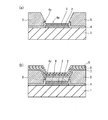
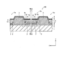
- FIG. 6 is an end view for explaining a process for obtaining one embodiment of the present invention. It is a top view which shows a part of organic electroluminescent display which concerns on embodiment of this invention. It is an end view which shows typically the partial cross section of the organic electroluminescent display which concerns on embodiment of this invention.
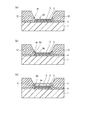
- FIG. 4 is an enlarged end view of a portion B surrounded by a one-dot chain line in FIG. 3. It is process drawing explaining the manufacturing method of the organic electroluminescent display which concerns on embodiment of this invention. It is process drawing explaining the manufacturing method of the organic electroluminescent display which concerns on embodiment of this invention. It is process drawing explaining the manufacturing method of the organic electroluminescent display which concerns on embodiment of this invention. It is process drawing explaining the manufacturing method of the organic electroluminescent display which concerns on embodiment of this invention.
- the inventor of the present invention relates to an organic EL element to which a metal compound is applied, as described in the “Background Art” section, and through extensive research, there is a possibility that the lifetime of the light emitting surface may be reduced due to generation of uneven brightness or local deterioration. I found something new.
- FIG. 1 is an end view showing a manufacturing process of an organic EL display.
- FIG. 1A shows a state where the first electrode 2, the ITO layer 3, the hole injection layer 4, and the bank 5 are formed on the TFT substrate 1.
- FIG. 1B shows a state in which the light emitting layer 6, the electron injection layer 7, the second electrode 8, and the sealing layer 9 are further formed.
- the recess 4a is formed on the upper surface of the hole injection layer 4 in the process of forming the bank 5 (FIG. 1A). reference).
- the electric field is concentrated near the edge 4c of the recess during light emission.
- a current may flow locally in the light emitting layer 6, and the generation of this local current may cause a problem of shortening the lifetime due to uneven brightness in the light emitting surface or local deterioration. is there.
- the inventor has covered the edge of the recess formed in the charge injecting and transporting layer with a part of the bank, thereby reducing the concentration of charges near the edge of the recess during light emission. As a result, it was possible to conceive the technical feature of suppressing the local current flow in the light emitting layer.
- a stacked body of at least a charge injecting and transporting layer and a functional layer including a light-emitting layer is interposed between a first electrode and a second electrode, and is defined by a bank.
- the light emitting layer is present in the formed region, and is a double-sided light emitting element that takes out light from both the first electrode side and the second electrode side, and the first electrode and the second electrode are transparent
- the charge injecting and transporting layer is formed in an indented structure whose upper surface is sunk in a region defined by the bank, and the edge of the recess in the indented structure of the charge injecting and transporting layer is a part of the bank. It is set as the structure coat
- the edge of the recess formed in the charge injecting and transporting layer is covered with a part of the bank, it is possible to suppress the concentration of the electric field on the edge of the recess during light emission. It can suppress that an electric current flows into a light emitting layer locally. Therefore, luminance unevenness in the light emitting surface can be suppressed, and the light emission characteristics can be further improved.
- the material constituting the charge injection / transport layer may be a metal oxide, nitride, or oxynitride. These materials are generally hydrophilic. Therefore, the recess can be formed in the cleaning step with pure water during the step of forming the bank.
- the functional layer includes a hole transport layer that transports holes from the hole injection layer to the light emitting layer, and the hole transport layer includes the hole injection layer and It can also be set as the structure interposed between the said light emitting layers.
- the transparent electrode may be ITO or IZO.
- a translucent or transparent metal thin film can be laminated on at least one of the first electrode and the second electrode.
- the translucent or transparent metal thin film is a metal film containing any one selected from Ag, Mg, Al, Pt, Pd, Au, Ni, Ir, and Cr.
- the film thickness may be 3 nm to 30 nm.
- the material constituting the charge injecting and transporting layer may be a material eroded by the liquid used when forming the bank.
- the liquid may be water or a TMAH solution.
- a part of the bank reaches the bottom surface of the recess in the recessed structure of the charge injection transport layer, and the side surface of the bank rises from the point reaching the bottom surface of the recess to the top. It may be a slope.
- a part of the bank may not reach the bottom surface of the concave portion in the concave structure of the charge injection transport layer.
- the bank material may be fluidized by applying heat treatment to the bank material so that the edge of the recess is covered with a part of the bank material. It is done. According to the above configuration, the bank material does not have to flow to the bottom of the recess, so that the temperature and time of the heat treatment can be reduced to a short time.
- the bank may include an insulating material. Thereby, adjacent light emitting layers can be insulated.
- the light emitting layer may be an organic EL layer.
- the charge injecting and transporting layer may extend to the side of the bank along the bottom surface of the bank.
- the edge of the concave portion of the charge injecting and transporting layer is a convex corner portion formed by a region not recessed in the upper surface of the charge injecting and transporting layer and a side surface of the concave portion. It is good as well.
- a light-emitting device which is one embodiment of the present invention can include a plurality of the above light-emitting elements.
- a method for manufacturing a light-emitting element which is one embodiment of the present invention includes at least a charge injecting and transporting layer and a functional layer including a light-emitting layer between a first electrode and a second electrode.
- a method of manufacturing a double-sided light emitting device in which the light emitting layer is present in a region defined by a bank and light is extracted from both the first electrode side and the second electrode side A step of forming the first electrode made of a transparent electrode, a step of forming a charge injection transport layer, and a step of forming a bank material layer made of a material constituting a bank on the charge injection transport layer.
- the charge injecting and transporting layer is used in a liquid used in a state where a part of the charge injecting and transporting layer is exposed, and the step of forming the second electrode made of a transparent electrode.
- the exposed surface of the charge injecting and transporting layer is formed into a recessed structure that is sunk from the level of the bottom of the remaining portion of the bank material layer due to the erosion of the liquid, and in the heat treatment step, By imparting fluidity to the remaining portion of the bank material layer, the material constituting the bank is extended from the remaining portion to the edge of the recessed portion of the recessed structure.
- the charge injection / transport layer may be a hole injection layer made of a metal oxide, nitride, or oxynitride.
- the functional layer includes a hole transport layer that transports holes from the hole injection layer to the light-emitting layer, and the hole transport layer includes the hole injection layer. It can also be interposed between the light emitting layer.
- ITO or IZO may be provided as the transparent electrode.
- a step of laminating a translucent or transparent metal thin film on at least one of the first electrode and the second electrode can be included.
- the translucent or transparent metal thin film is a metal film containing any one selected from Ag, Mg, Al, Pt, Pd, Au, Ni, Ir, and Cr.
- the film thickness can be 3 nm to 30 nm.
- the metal film can be formed by a vacuum process.
- an organic EL element using an organic EL material for a light emitting layer will be described as a light emitting element
- an organic EL display will be described as an example of a light emitting device provided with a plurality of light emitting elements.
- the scale of the member in each drawing differs from an actual thing.
- FIG. 2 is a plan view showing a part of a double-sided light emitting organic EL display according to an embodiment of the present invention.
- the organic EL display 100 is a double-sided light emitting organic EL display in which organic EL elements 10a, 10b, and 10c each having an RGB light emitting layer are arranged in a matrix. Each organic EL element functions as a sub-pixel, and a set of three organic EL elements of RGB functions as a pixel.
- a cross-shaped pixel bank 55 is adopted, and the light emitting layers 56 a 1, 56 b 1, 56 c 1 adjacent in the X axis direction are divided by the bank elements 55 a extending in the Y axis direction, and the light emitting layer 56a2, 56b2, and 56c2 are divided.
- the bank elements 55b extending in the X-axis direction divide the light emitting layers 56a1 and 56a2 adjacent in the Y-axis direction, the light emitting layers 56b1 and 56b2, and the light emitting layers 56c1 and 56c2.
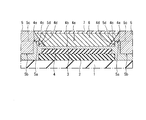
- FIG. 3 is an end view schematically showing a partial cross section of the organic EL display according to the embodiment of the present invention, and shows a cross section taken along line AA of FIG.
- FIG. 4 is an enlarged end view of a portion B surrounded by an alternate long and short dash line in FIG.
- a first electrode 2 as an anode is formed in a matrix on a TFT substrate 1 (hereinafter simply “substrate 1”).
- An ITO (indium tin oxide) layer 3 and a hole are formed on the first electrode 2.
- the injection layer 4 is laminated in that order.
- the ITO layer 3 is laminated only on the first electrode 2, whereas the hole injection layer 4 is formed not only on the first electrode 2 but over the entire upper surface of the substrate 1.
- a bank 5 is formed on the upper periphery of the first electrode 2 via a hole injection layer 4, and a light emitting layer 6 is laminated in a region defined by the bank 5. Further, on the light emitting layer 6, an electron injection layer 7, a second electrode 8 that is a cathode, and a sealing layer 9 are adjacent to the organic EL elements 10 a, 10 b, beyond the region defined by the bank 5, respectively. 10c is formed so as to be continuous. During driving, light emission can be extracted from both the first electrode 2 side and the second electrode 8 side.
- the substrate 1 is, for example, alkali-free glass, soda glass, non-fluorescent glass, phosphoric acid glass, boric acid glass, quartz, acrylic resin, styrene resin, polycarbonate resin, epoxy resin, polyethylene, polyester, silicone resin. Or an insulating material such as alumina.
- the first electrode 2 is a transparent electrode, and in addition to metal oxides such as ITO and IZO, APC (silver, palladium, copper alloy), ARA (silver, rubidium, gold alloy), MoCr (molybdenum and chromium alloy). Alloy), NiCr (nickel and chromium alloy) and the like.
- metal oxides such as ITO and IZO, APC (silver, palladium, copper alloy), ARA (silver, rubidium, gold alloy), MoCr (molybdenum and chromium alloy). Alloy), NiCr (nickel and chromium alloy) and the like.
- it may be a metal film containing any one selected from Ag, Mg, Al, Pt, Pd, Au, Ni, Ir, and Cr.
- the film is formed with an appropriate thickness (for example, a film thickness of 3 nm to 30 nm).
- the first electrode 2 and the second electrode 8 to be described later are both transparent electrodes, but have a certain light transmittance.
- a “semi-transparent or transparent” thin film and I can say that.
- a metal material generally known as opaque can be a translucent or transparent film that can exhibit light transmittance if the film thickness is sufficiently reduced as described above.
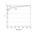
- FIG. 12 is a graph showing the relationship between transmittance (T%) and wavelength for tungsten oxide (Wox) having a thickness of 12 nm and 15 nm.
- T% transmittance
- Wox tungsten oxide
- a transmittance of 85% or more can be obtained for light in a wide wavelength range from 350 nm to 650 nm if at least the thickness is set in the range of 12 nm to 15 nm.
- an Mg—Ag alloy electrode having a film thickness set to 5 to 40 nm.
- Patent Document 2 shows that good transparency can be obtained by setting the cathode to a thickness of 10 to 800 nm. Considering these findings, it is considered that sufficient transparency can be obtained if the thickness of each metal material of the first electrode 2 and the second electrode 8 is set to about 3 nm to 30 nm.
- the ITO layer 3 is interposed between the first electrode 2 and the hole injection layer 4 and has a function of improving the bonding property between the layers.
- the hole injection layer 4 is formed of WOx (tungsten oxide) or MoxWyOz (molybdenum-tungsten oxide).
- the hole injection layer 4 should just be formed with the metal compound which performs a hole injection function, As such a metal compound, a metal oxide, a metal nitride, or a metal oxynitride is mentioned, for example.
- the hole injection layer 4 When the hole injection layer 4 is formed of a specific metal compound, holes can be easily injected, and electrons can effectively contribute to light emission in the light emitting layer 6, so that good light emission characteristics can be obtained. it can.
- a specific metal compound a transition metal is preferable. Since the transition metal takes a plurality of oxidation numbers, it can take a plurality of levels. As a result, hole injection becomes easy and the driving voltage can be reduced.
- the hole injection layer 4 extends laterally along the bottom surfaces 5a and 5b of the bank 5, and a part of the top surface is recessed to form a recess 4a.
- a bottom surface 4b as an inner bottom surface portion of the recess 4a is depressed below the level 5c of the bank bottom surface 5a.
- the recess 4a includes a bottom surface 4b and a side surface 4d as an inner side surface continuous with the bottom surface 4b.
- the depth of the recess 4a is approximately 5 nm to 30 nm. Therefore, since the hole injection layer 4 is composed of a metal oxide thin film having a sufficient thickness like the first electrode 2, it has good transparency as described above with reference to FIG. .
- the edge 4c of the recess is a convex corner portion formed by the region 4e that is not recessed on the upper surface of the hole injection layer 4 and the side surface 4d of the recess, and is covered with the covering portion 5d that is a part of the bank 5. Yes.
- the edge 4c of the recess protrudes with respect to the bottom surface 4b of the recess, if the edge 4c of the recess is not covered with the insulating covering portion 5d, an electric field concentration occurs and the light emitting layer 6 is locally localized. As a result, current flows, and as a result, there is a problem that the life of the product is shortened due to uneven brightness in the light emitting surface and local deterioration of the light emitting layer 6.
- the edge 4c of the recess is covered with the insulating covering portion 5d, it is possible to suppress the occurrence of such a problem.
- the thickness of the covering portion 5d (the shortest distance from the edge 4c of the recess to the light emitting layer 6) be 2 nm to 5 nm.
- the shape of the edge 4c of the recess is made polygonal or rounded rather than the edge shape as shown in FIG. 4 as an example, so that electric field concentration can be further suppressed.
- the covering portion 5d reaches the bottom surface 4b of the recess 4a, and the side surface of the bank 5 is an upward slope from the point reaching the recess bottom surface 4b to the apex.
- the bank 5 is for partitioning the light emitting layer 6 for each sub-pixel, and is formed of an organic material such as resin and has an insulating property.
- organic materials include acrylic resins, polyimide resins, novolac type phenol resins, and the like.
- the bank 5 preferably has organic solvent resistance. Furthermore, since the bank 5 may be subjected to an etching process, a baking process, or the like, it is preferable that the bank 5 be formed of a highly resistant material that does not excessively deform or alter the process.
- the light emitting layer 6 constitutes a functional layer.
- a functional layer for example, an oxinoid compound, a perylene compound, a coumarin compound, an azacoumarin compound, an oxazole compound, an oxadiazole compound, a perinone compound, a pyrrolopyrrole compound described in JP-A-5-163488, Naphthalene compounds, anthracene compounds, fluorene compounds, fluoranthene compounds, tetracene compounds, pyrene compounds, coronene compounds, quinolone compounds and azaquinolone compounds, pyrazoline derivatives and pyrazolone derivatives, rhodamine compounds, chrysene compounds, phenanthrene compounds, cyclopentadiene compounds, stilbene compounds, diphenyl Quinone compound, styryl compound, butadiene compound, dicyanomethylenepyran compound, dicyanomethylenethiopyran compound, fluorescein Compound
- the electron injection layer 7 has a function of transporting electrons injected from the second electrode 8 to the light emitting layer 6, and is preferably formed of, for example, barium, phthalocyanine, lithium fluoride, or a combination thereof.
- the second electrode 8 is made of the same transparent electrode material as that of the first electrode 2 and has an appropriate film thickness (3 nm to 30 nm) so as to exhibit good light transmittance by the same method as the first electrode 2. Composed.
- the sealing layer 9 has a function of preventing the light emitting layer 6 and the like from being exposed to moisture or air, and is made of, for example, a material such as SiN (silicon nitride) or SiON (silicon oxynitride). It is formed.
- metal compounds generally have a property of absorbing visible light at a certain ratio, when light emitted from the light emitting layer is extracted outside through the charge injecting and transporting layer, light is absorbed, resulting in a loss of light emission efficiency. There is.
- the non-light emitting region is a region that does not contribute to light emission, and becomes a simple transparent substrate. Therefore, the background of the light emitting element is seen through, and there is a problem that the display performance of the light emitting element or the display panel using the light emitting element is deteriorated.
- the light emitting layer 6 is formed in the concave portion 4a of the charge injection transport layer (hole injection layer 4) whose upper surface is sunk.
- the recess 4a having a relatively small thickness in the hole injection layer 4 it is possible to reduce the absorption ratio of light emission from the light emitting layer 6 generated during driving.
- the light transmittance at a wavelength of 400 nm is 95% when the tungsten oxide film thickness is 12 nm, and 93% when 15 nm.
- the light transmittance at a wavelength of 450 nm is 97% when the tungsten oxide film thickness is 12 nm and 95% when the film thickness is 15 nm.
- the light transmittance at a wavelength of 530 nm is 98% when the tungsten oxide film thickness is 12 nm, and 97% when the film thickness is 15 nm.
- the light transmittance of a device such as an organic EL display having a structure in which a plurality of films are stacked is represented by the product of the light transmittance of each layer. Therefore, it is important to improve the light transmittance of each layer so that the light transmittance approaches 100%. In particular, when blue light emission is difficult to develop, it is possible to expect an effective improvement in light transmittance by applying this embodiment in order to improve the light emission efficiency. It is effective as an improvement measure. As described above, if the inside of the region of the charge injection / transport layer defined by the bank has a recessed structure, the light transmittance of the light emitting region can be improved, and a double-sided light emitting element can be realized well.
- the depth of the recess 4a (recessed structure) is preferably about 5 nm to 30 nm.
- the edge of the recess 4a of the hole injection layer 4 is covered with a part of the bank 5, thereby preventing local light emission in the light emitting surface and uniform over the entire desired light emitting region.
- Light emission can be expected.
- a region that does not contribute to light emission is not formed in the light emitting surface, light generated in the light emitting layer is extracted to the outside with excellent luminous efficiency over both the upper surface and the lower surface (see arrows in FIG. 3). .
- desired light emission or display can be realized without transmitting the background of the double-sided light emitting element.
- ⁇ Manufacturing method> 5 to 7 are process diagrams illustrating a method for manufacturing an organic EL display according to an embodiment of the present invention.
- a first electrode 2 is formed on a substrate 1 using a vacuum process.
- a vacuum process a known process such as a vacuum deposition method, sputtering, an electron beam method, a CVD method, or ion plating can be used.
- a sputtering apparatus using a known DC magnetron sputtering method is used.
- the chamber is filled with an inert gas such as argon gas at a predetermined pressure (for example, 3 ⁇ 10 ⁇ 1 Pa), and a film is uniformly formed on the surface of the substrate 1.
- the first electrode 2 is formed in a matrix by patterning the Ag thin film by photolithography.
- a resistance heating type is suitable. Specifically, vapor deposition pellets or particles containing a predetermined transparent electrode material are placed in a resistance heating boat or resistance heating filament of a vacuum evaporation apparatus. Then, the substrate 1 is attached to a predetermined substrate holder, the inside of the chamber is decompressed to 5 ⁇ 10 ⁇ 4 Pa, the substrate temperature is heated to about 10 to 100 ° C., and the deposition rate is set to 20 nm / sec or less to form a film. carry out. Thereafter, as described above, the deposited film is patterned.
- an ITO thin film is formed by a vacuum process (for example, sputtering) similar to the first electrode 2, and the ITO thin film is patterned by, for example, photolithography to form an ITO layer 3 To do.
- a vacuum process for example, sputtering
- a thin film 11 of WOx or MoxWyOz is formed by a technique such as vacuum deposition or sputtering in the same manner as the first electrode 2.
- a bank material layer 12 is formed on the thin film 11 using a bank material made of an organic material, and a part of the bank material layer 12 is removed to remove a part of the thin film 11. To expose.
- the bank material layer 12 can be formed, for example, by coating. The removal of the bank material layer 12 can be performed by patterning using a predetermined developer (tetramethylammonium hydroxide (TMAH) solution or the like).
- TMAH tetramethylammonium hydroxide
- heat treatment is performed to give a certain degree of fluidity to the remaining portion of the bank material layer 12, and the bank material is extended from the remaining portion to the edge 4c of the recess. As a result, the edge 4c of the recess is covered with the covering portion 5d.
- heat curing can be employed for the heat treatment. The temperature and time of the heat curing may be appropriately determined in consideration of the type of bank material, the required thickness of the covering portion 5d, and the like.
- the surface of the remaining portion of the bank material layer 12 is subjected to a liquid repellent treatment using, for example, fluorine plasma to form the bank 5.
- a composition ink (hereinafter simply referred to as “ink”) containing an organic EL material is dropped into the region defined by the bank 5 by, for example, an ink jet method. Is dried to form the light emitting layer 6.
- the ink may be dropped by a dispenser method, a nozzle coating method, a spin coating method, intaglio printing, letterpress printing, or the like.
- a barium thin film to be the electron injection layer 7 is formed by, for example, vacuum deposition.
- an ITO thin film to be the second electrode 8 is formed by a vacuum process similar to that for the first electrode 2, for example.
- the second electrode 8 can be formed by sputtering or vacuum deposition method in which the heating temperature of the substrate 1 is relatively low in consideration of thermal influence and simplicity. Is preferred. However, attention should be paid to the deposition strength so that the light emitting layer 6 is not damaged by the plasma generated by the sputtering.
- a sealing layer 9 is further formed.
- the manufacturing method even if the recessed portion 4a is formed in the exposed portion of the hole injection layer 4 in the manufacturing process, the edge 4c of the recessed portion is covered with the covering portion 5d, and then the light emitting layer 6 is formed. It is possible to suppress the concentration of the electric field on the edge 4c of the recess.
- the metal oxide layer (thin film 11) having a uniform thickness is formed, a part of the surface portion is dissolved during the cleaning of the bank residue using the developer, and the concave portion is formed.
- the thickness portion in the light emitting region is reduced, and the hole injection layer 4 is formed.
- the surface is partially dissolved to form a concave structure, so that the charge injection and transport performance is excellent, and the light emitting region Then, since the thin hole injection layer 4 can be produced efficiently, it is advantageous.
- this invention is not limited to these embodiment.
- the following modifications can be considered.
- WOx or MoxWyOz is used as the material constituting the hole injection layer 4, but generally, metal oxides, nitrides, and oxynitrides are easily eroded by pure water. Even when a metal other than Mo (molybdenum) and W (tungsten) is used, the same effect can be obtained by applying this embodiment.
- the hole injection layer is eroded by pure water during cleaning to form a recess, but if the present invention is adopted, even if the recess is formed for other reasons, An effect of suppressing the concentration of the electric field on the edge of the recess can be obtained.
- Other reasons include, for example, the case where the hole injection layer is eroded by an etching solution during etching or the case where the hole injection layer is eroded by a stripping agent during resist stripping. In this way, when the hole injection layer is made of a material eroded by the liquid used when forming the bank, more specifically, the material eroded by the liquid used with a part of the hole injection layer exposed.
- the present invention is effective when consisting of: (3)
- the covering portion extending from the bank reaches the bottom surface 4b of the concave portion beyond the edge 4c of the concave portion.
- the present invention only needs to cover the edge 4c of the concave portion.
- the covering portion 5 d may not reach the bottom surface 4 b of the recess.
- the bank material does not have to flow to the bottom of the recess, so that the heat treatment temperature and time can be reduced to a short time.
- the present invention can use max patterning as another forming method. . (4)
- the lower end of the slope of the bank material 12 and the edge 4c of the recess coincide, but this is not necessarily the case.
- the slope of the bank material 12 may recede to expose a part of the non-recessed region 4e. Even in this case, the bank material 12 may be appropriately heat-treated so that the edge 4c of the recess is covered with a part of the bank material (see FIG. 9B).
- a hole transport layer 13 may be formed on the hole injection layer 4, and these may be inserted as a charge injection transport layer.
- a recess is formed on the upper surface of the hole transport layer 13, and the edge of the recess formed in the hole transport layer is covered with the covering portion.
- the charge injection / transport layer may be composed of only the hole injection layer, and the hole injection layer and the hole transport layer constituting the functional layer may be interposed between the first electrode and the light emitting layer.
- the hole 4 c on the recess 4 a of the hole injection layer 4 is formed on the recess 4 a of the hole injection layer 4 with the edge 4 c of the recess 4 a of the hole injection layer 4 covered with the cover 5 d of the bank 5.
- the hole transport layer 13 may be formed by applying an ink containing a transport material
- the light emitting layer 6 may be formed by applying an ink containing a light emitting material on the hole transport layer 13.
- the ITO layer 3 is formed thereon.
- the ITO layer 3 can be eliminated and the anode can have a single layer structure.
- an organic EL display is described as an example of a light-emitting device including a plurality of light-emitting elements, but the present invention is not limited to this and can be applied to a lighting device or the like.
- a so-called pixel bank is used, but the present invention is not limited to this.
- a line bank line-shaped bank
- the line bank 65 is employed, and the light emitting layers 66a, 66b, 66c adjacent in the X-axis direction are divided. As shown in FIG. 11, when the line bank 65 is adopted, the light emitting layers adjacent in the Y-axis direction are not defined by the bank elements, but the driving method, the size and interval of the anode, etc. are set appropriately. By doing so, it is possible to emit light without affecting each other. (9) In the above embodiment, only the electron injection layer is interposed between the light emitting layer and the second electrode, but in addition to this, an electron transport layer may be interposed. (10) In the above embodiment, an organic material is used as the bank material, but an inorganic material can also be used.
- the bank material layer can be formed by coating, for example, as in the case of using an organic material.
- the removal of the bank material layer can be performed by forming a resist pattern on the bank material layer and then performing etching using a predetermined etching solution (tetramethylammonium hydroxide oxide (TMAH) solution or the like).
- TMAH tetramethylammonium hydroxide oxide
- the resist pattern is removed after etching by, for example, an aqueous or non-aqueous release agent. Next, the etching residue is washed with pure water.
- the material constituting the thin film WOx or MoxWyOz
- the exposed portion of the thin film is eroded to form a concave structure as in the case shown in FIG. It is formed.
- a hole injection layer having a recess is formed.
- the present invention can be applied as in the case where an organic material is used.
- the present invention can be used for an organic EL display or the like.
Landscapes
- Physics & Mathematics (AREA)
- Optics & Photonics (AREA)
- Electroluminescent Light Sources (AREA)
Abstract
La présente invention concerne un dispositif émetteur de lumière possédant de bonnes caractéristiques d'émission de lumière, un appareil émettant de la lumière équipé dudit dispositif, et un procédé de fabrication d'un dispositif émetteur de lumière. Plus spécifiquement, la construction suivante est adoptée. Des dispositifs électroluminescents organiques (10a), (10b) et (10c) sont configurés en empilant au moins une couche d'injection de trous (4) et une couche d'émission de lumière (6) entre une première électrode (2) et une deuxième électrode (8) mutuellement transparentes. La couche d'émission de lumière (6) se situe dans une région délimitée par des talus (5). Dans cette configuration, la couche d'injection de trous (4) dans la région délimitée par des talus (5) est formée en creux, de sorte que sa surface supérieure se retrouve plus bas. Le bord (4c) de la partie en creux de la couche d'injection de trous (4) est recouvert par une partie des talus (5).
Priority Applications (3)
| Application Number | Priority Date | Filing Date | Title |
|---|---|---|---|
| PCT/JP2010/004986 WO2012017496A1 (fr) | 2010-08-06 | 2010-08-06 | Dispositif émetteur de lumière, appareil émettant de la lumière équipé dudit dispositif, et procédé de fabrication d'un dispositif émetteur de lumière |
| JP2012527473A JP5620495B2 (ja) | 2010-08-06 | 2010-08-06 | 発光素子、発光素子を備えた発光装置および発光素子の製造方法 |
| US13/746,481 US8890129B2 (en) | 2010-08-06 | 2013-01-22 | Light emitting device, light emitting apparatus provided with a light emitting device, and method of manufacturing a light emitting device |
Applications Claiming Priority (1)
| Application Number | Priority Date | Filing Date | Title |
|---|---|---|---|
| PCT/JP2010/004986 WO2012017496A1 (fr) | 2010-08-06 | 2010-08-06 | Dispositif émetteur de lumière, appareil émettant de la lumière équipé dudit dispositif, et procédé de fabrication d'un dispositif émetteur de lumière |
Related Child Applications (1)
| Application Number | Title | Priority Date | Filing Date |
|---|---|---|---|
| US13/746,481 Continuation US8890129B2 (en) | 2010-08-06 | 2013-01-22 | Light emitting device, light emitting apparatus provided with a light emitting device, and method of manufacturing a light emitting device |
Publications (1)
| Publication Number | Publication Date |
|---|---|
| WO2012017496A1 true WO2012017496A1 (fr) | 2012-02-09 |
Family
ID=45559029
Family Applications (1)
| Application Number | Title | Priority Date | Filing Date |
|---|---|---|---|
| PCT/JP2010/004986 Ceased WO2012017496A1 (fr) | 2010-08-06 | 2010-08-06 | Dispositif émetteur de lumière, appareil émettant de la lumière équipé dudit dispositif, et procédé de fabrication d'un dispositif émetteur de lumière |
Country Status (3)
| Country | Link |
|---|---|
| US (1) | US8890129B2 (fr) |
| JP (1) | JP5620495B2 (fr) |
| WO (1) | WO2012017496A1 (fr) |
Families Citing this family (6)
| Publication number | Priority date | Publication date | Assignee | Title |
|---|---|---|---|---|
| US9299956B2 (en) * | 2012-06-13 | 2016-03-29 | Aixtron, Inc. | Method for deposition of high-performance coatings and encapsulated electronic devices |
| KR102173510B1 (ko) | 2014-05-20 | 2020-11-04 | 엘지디스플레이 주식회사 | 유기전계발광소자 |
| CN104765157B (zh) * | 2015-05-06 | 2017-12-08 | 京东方科技集团股份有限公司 | 显示面板及其显示方法、显示装置 |
| CN107863458B (zh) * | 2017-10-30 | 2019-11-15 | 武汉华星光电半导体显示技术有限公司 | Oled基板的制作方法及oled显示装置的制作方法 |
| CN108565352B (zh) * | 2018-04-19 | 2020-02-21 | 京东方科技集团股份有限公司 | 有机发光二极管显示面板及其制造方法、显示装置 |
| KR102763305B1 (ko) * | 2019-11-26 | 2025-02-05 | 삼성디스플레이 주식회사 | 표시 장치 |
Citations (3)
| Publication number | Priority date | Publication date | Assignee | Title |
|---|---|---|---|---|
| JP2005267926A (ja) * | 2004-03-17 | 2005-09-29 | Japan Science & Technology Agency | 両面発光有機elパネル |
| JP2009004347A (ja) * | 2007-05-18 | 2009-01-08 | Toppan Printing Co Ltd | 有機el表示素子の製造方法及び有機el表示素子 |
| JP2009218156A (ja) * | 2008-03-12 | 2009-09-24 | Casio Comput Co Ltd | Elパネル及びelパネルの製造方法 |
Family Cites Families (113)
| Publication number | Priority date | Publication date | Assignee | Title |
|---|---|---|---|---|
| US5443922A (en) | 1991-11-07 | 1995-08-22 | Konica Corporation | Organic thin film electroluminescence element |
| JPH05163488A (ja) | 1991-12-17 | 1993-06-29 | Konica Corp | 有機薄膜エレクトロルミネッセンス素子 |
| US5294869A (en) | 1991-12-30 | 1994-03-15 | Eastman Kodak Company | Organic electroluminescent multicolor image display device |
| US5688551A (en) | 1995-11-13 | 1997-11-18 | Eastman Kodak Company | Method of forming an organic electroluminescent display panel |
| DE69729394T2 (de) | 1996-11-29 | 2005-06-02 | Idemitsu Kosan Co. Ltd. | Organische elektrolumineszente Vorrichtung |
| JPH10162959A (ja) | 1996-11-29 | 1998-06-19 | Idemitsu Kosan Co Ltd | 有機エレクトロルミネッセンス素子 |
| JP3782245B2 (ja) | 1998-10-28 | 2006-06-07 | Tdk株式会社 | 有機el表示装置の製造装置及び製造方法 |
| US6309801B1 (en) | 1998-11-18 | 2001-10-30 | U.S. Philips Corporation | Method of manufacturing an electronic device comprising two layers of organic-containing material |
| JP4198253B2 (ja) | 1999-02-02 | 2008-12-17 | 出光興産株式会社 | 有機エレクトロルミネッセンス素子およびその製造方法 |
| JP2002075661A (ja) | 2000-08-31 | 2002-03-15 | Fujitsu Ltd | 有機el素子及び有機el表示装置 |
| US7153592B2 (en) | 2000-08-31 | 2006-12-26 | Fujitsu Limited | Organic EL element and method of manufacturing the same, organic EL display device using the element, organic EL material, and surface emission device and liquid crystal display device using the material |
| TWI257496B (en) | 2001-04-20 | 2006-07-01 | Toshiba Corp | Display device and method of manufacturing the same |
| JP2002318556A (ja) | 2001-04-20 | 2002-10-31 | Toshiba Corp | アクティブマトリクス型平面表示装置およびその製造方法 |
| US8058797B2 (en) | 2001-05-18 | 2011-11-15 | Cambridge University Technical Services Limited | Electroluminescent device |
| JP2003007460A (ja) | 2001-06-22 | 2003-01-10 | Sony Corp | 表示装置の製造方法および表示装置 |
| JP3823916B2 (ja) | 2001-12-18 | 2006-09-20 | セイコーエプソン株式会社 | 表示装置及び電子機器並びに表示装置の製造方法 |
| JP2003264083A (ja) | 2002-03-08 | 2003-09-19 | Sharp Corp | 有機led素子とその製造方法 |
| US7086917B2 (en) * | 2002-08-12 | 2006-08-08 | National Research Council Of Canada | Photoresist mask/smoothing layer ensuring the field homogeneity and better step-coverage in OLED displays |
| JP4165173B2 (ja) | 2002-10-15 | 2008-10-15 | 株式会社デンソー | 有機el素子の製造方法 |
| JP2004228355A (ja) | 2003-01-23 | 2004-08-12 | Seiko Epson Corp | 絶縁膜基板の製造方法、絶縁膜基板の製造装置及び絶縁膜基板並びに電気光学装置の製造方法及び電気光学装置 |
| JP2004234901A (ja) | 2003-01-28 | 2004-08-19 | Seiko Epson Corp | ディスプレイ基板、有機el表示装置、ディスプレイ基板の製造方法および電子機器 |
| EP1629544B1 (fr) | 2003-05-12 | 2008-11-19 | Cambridge Enterprise Limited | Transistor polymere |
| ATE401672T1 (de) | 2003-05-12 | 2008-08-15 | Cambridge Entpr Ltd | Herstellung einer polymeren vorrichtung |
| JP2005012173A (ja) | 2003-05-28 | 2005-01-13 | Seiko Epson Corp | 膜パターン形成方法、デバイス及びデバイスの製造方法、電気光学装置、並びに電子機器 |
| JP2004363170A (ja) | 2003-06-02 | 2004-12-24 | Seiko Epson Corp | 導電パターンの形成方法、電気光学装置、電気光学装置の製造方法および電子機器 |
| US7492090B2 (en) | 2003-09-19 | 2009-02-17 | Semiconductor Energy Laboratory Co., Ltd. | Display device and method for manufacturing the same |
| US7230374B2 (en) * | 2003-09-22 | 2007-06-12 | Samsung Sdi Co., Ltd. | Full color organic light-emitting device having color modulation layer |
| US20060139342A1 (en) | 2004-12-29 | 2006-06-29 | Gang Yu | Electronic devices and processes for forming electronic devices |
| JP2005203340A (ja) | 2003-12-16 | 2005-07-28 | Matsushita Electric Ind Co Ltd | 有機エレクトロルミネッセント素子 |
| US20090160325A1 (en) | 2003-12-16 | 2009-06-25 | Panasonic Corporation | Organic electroluminescent device and method for manufacturing the same |
| JP2005203339A (ja) | 2003-12-16 | 2005-07-28 | Matsushita Electric Ind Co Ltd | 有機エレクトロルミネッセント素子およびその製造方法 |
| KR20060110323A (ko) | 2003-12-16 | 2006-10-24 | 마츠시타 덴끼 산교 가부시키가이샤 | 유기 전기발광 소자 및 그 제조 방법 |
| JP4857521B2 (ja) | 2004-01-09 | 2012-01-18 | セイコーエプソン株式会社 | 電気光学装置の製造方法、電気光学装置、及び電子機器 |
| JP2005268099A (ja) | 2004-03-19 | 2005-09-29 | Mitsubishi Electric Corp | 有機el表示パネル、有機el表示装置、および有機el表示パネルの製造方法 |
| JP4645064B2 (ja) | 2004-05-19 | 2011-03-09 | セイコーエプソン株式会社 | 電気光学装置の製造方法 |
| US7541099B2 (en) | 2004-05-21 | 2009-06-02 | Semiconductor Energy Laboratory Co., Ltd. | Anthracene derivative and light emitting element and light emitting device using the same |
| JP4161956B2 (ja) * | 2004-05-27 | 2008-10-08 | セイコーエプソン株式会社 | カラーフィルタ基板の製造方法、電気光学装置の製造方法、電気光学装置、電子機器 |
| US7211456B2 (en) | 2004-07-09 | 2007-05-01 | Au Optronics Corporation | Method for electro-luminescent display fabrication |
| JP2006185869A (ja) | 2004-12-28 | 2006-07-13 | Asahi Glass Co Ltd | 有機電界発光素子及びその製造方法 |
| DE102005007540A1 (de) | 2005-02-18 | 2006-08-31 | Robert Bosch Gmbh | Mikromechanischer Membransensor mit Doppelmembran |
| JP2006253443A (ja) | 2005-03-11 | 2006-09-21 | Seiko Epson Corp | 有機el装置、その製造方法および電子機器 |
| JP2006294261A (ja) | 2005-04-05 | 2006-10-26 | Fuji Electric Holdings Co Ltd | 有機el発光素子およびその製造方法 |
| JP2006344459A (ja) | 2005-06-08 | 2006-12-21 | Sony Corp | 転写方法および転写装置 |
| TWI307612B (en) | 2005-04-27 | 2009-03-11 | Sony Corp | Transfer method and transfer apparatus |
| JP2007073499A (ja) | 2005-08-08 | 2007-03-22 | Semiconductor Energy Lab Co Ltd | 発光装置およびその作製方法 |
| US7994711B2 (en) | 2005-08-08 | 2011-08-09 | Semiconductor Energy Laboratory Co., Ltd. | Light emitting device and manufacturing method thereof |
| GB0517195D0 (en) * | 2005-08-23 | 2005-09-28 | Cambridge Display Tech Ltd | Molecular electronic device structures and fabrication methods |
| JP4106076B2 (ja) | 2005-09-29 | 2008-06-25 | 松下電器産業株式会社 | 有機elディスプレイおよびその製造方法 |
| JP2007095606A (ja) | 2005-09-30 | 2007-04-12 | Seiko Epson Corp | 有機el装置、その製造方法、及び電子機器 |
| JP2007150258A (ja) | 2005-10-27 | 2007-06-14 | Seiko Epson Corp | パターン形成方法、膜構造体、電気光学装置及び電子機器 |
| JP4318689B2 (ja) | 2005-12-09 | 2009-08-26 | 出光興産株式会社 | n型無機半導体、n型無機半導体薄膜及びその製造方法 |
| JP5256605B2 (ja) | 2006-01-18 | 2013-08-07 | 凸版印刷株式会社 | 有機エレクトロルミネッセンス素子の製造方法 |
| JP2007214066A (ja) | 2006-02-13 | 2007-08-23 | Seiko Epson Corp | 有機エレクトロルミネセンス装置の製造方法 |
| JP2007287353A (ja) | 2006-04-12 | 2007-11-01 | Matsushita Electric Ind Co Ltd | 有機エレクトロルミネッセント素子の製造方法およびそれを用いて作成された有機エレクトロルミネッセント素子 |
| US20070241665A1 (en) | 2006-04-12 | 2007-10-18 | Matsushita Electric Industrial Co., Ltd. | Organic electroluminescent element, and manufacturing method thereof, as well as display device and exposure apparatus using the same |
| JP2007288074A (ja) | 2006-04-19 | 2007-11-01 | Matsushita Electric Ind Co Ltd | 有機エレクトロルミネッセント素子およびその製造方法 |
| JP2007288071A (ja) | 2006-04-19 | 2007-11-01 | Matsushita Electric Ind Co Ltd | 有機エレクトロルミネッセント素子およびその製造方法、それを用いた表示装置、露光装置 |
| JP2008041747A (ja) | 2006-08-02 | 2008-02-21 | Matsushita Electric Ind Co Ltd | 有機エレクトロルミネッセント発光装置およびその製造方法 |
| US20070290604A1 (en) | 2006-06-16 | 2007-12-20 | Matsushita Electric Industrial Co., Ltd. | Organic electroluminescent device and method of producing the same |
| JP4915650B2 (ja) | 2006-08-25 | 2012-04-11 | パナソニック株式会社 | 有機エレクトロルミネッセンス素子 |
| JP2008091072A (ja) | 2006-09-29 | 2008-04-17 | Seiko Epson Corp | 電気光学装置、およびその製造方法 |
| JP4915913B2 (ja) | 2006-11-13 | 2012-04-11 | パナソニック株式会社 | 有機エレクトロルミネッセンス素子 |
| JP2008140724A (ja) | 2006-12-05 | 2008-06-19 | Toppan Printing Co Ltd | 有機el素子の製造方法および有機el素子 |
| WO2008075615A1 (fr) | 2006-12-21 | 2008-06-26 | Semiconductor Energy Laboratory Co., Ltd. | Élément et dispositif électroluminescents |
| JP4998710B2 (ja) | 2007-03-06 | 2012-08-15 | カシオ計算機株式会社 | 表示装置の製造方法 |
| JP5326289B2 (ja) | 2007-03-23 | 2013-10-30 | 凸版印刷株式会社 | 有機el素子およびそれを備えた表示装置 |
| US8471461B2 (en) | 2007-03-29 | 2013-06-25 | Dai Nippon Printing Co., Ltd. | Organic electroluminescent device and method for producing the same |
| KR100919352B1 (ko) | 2007-05-30 | 2009-09-25 | 파나소닉 주식회사 | 유기 el 디스플레이 패널 및 그 제조 방법 |
| JP4280301B2 (ja) | 2007-05-31 | 2009-06-17 | パナソニック株式会社 | 有機el素子、およびその製造方法 |
| US20080312437A1 (en) | 2007-06-04 | 2008-12-18 | Semiconductor Energy Labratory Co., Ltd. | Organometallic Complex, and Light-Emitting Element, Light-Emitting Device, and Electronic Device Using the Organometallic Complex |
| US8628986B2 (en) | 2007-07-31 | 2014-01-14 | Sumitomo Chemical Company, Limited | Organic electroluminescent element and method for manufacturing the same |
| JP5001745B2 (ja) | 2007-08-10 | 2012-08-15 | 住友化学株式会社 | 有機エレクトロルミネッセンス素子及び製造方法 |
| JP2009048960A (ja) | 2007-08-23 | 2009-03-05 | Canon Inc | 電極洗浄処理方法 |
| JP2009058897A (ja) | 2007-09-03 | 2009-03-19 | Hitachi Displays Ltd | 表示装置 |
| US8083956B2 (en) | 2007-10-11 | 2011-12-27 | Semiconductor Energy Laboratory Co., Ltd. | Display device and method for manufacturing display device |
| JP2009135053A (ja) | 2007-11-30 | 2009-06-18 | Sumitomo Chemical Co Ltd | 電子デバイス、表示装置および電子デバイスの製造方法 |
| WO2009075075A1 (fr) | 2007-12-10 | 2009-06-18 | Panasonic Corporation | Dispositif électroluminescent organique, panneau d'affichage électroluminescent, procédé de fabrication du dispositif électroluminescent organique et procédé de fabrication du panneau d'affichage électroluminescent |
| JP4439589B2 (ja) | 2007-12-28 | 2010-03-24 | パナソニック株式会社 | 有機elデバイスおよび有機elディスプレイパネル、ならびにそれらの製造方法 |
| JP4418525B2 (ja) | 2008-02-28 | 2010-02-17 | パナソニック株式会社 | 有機elディスプレイパネル |
| JP5267246B2 (ja) | 2008-03-26 | 2013-08-21 | 凸版印刷株式会社 | 有機エレクトロルミネッセンス素子及びその製造方法並びに有機エレクトロルミネッセンス表示装置 |
| JP2009239180A (ja) | 2008-03-28 | 2009-10-15 | Sumitomo Chemical Co Ltd | 有機エレクトロルミネッセンス素子 |
| KR100999739B1 (ko) | 2008-04-02 | 2010-12-08 | 엘지이노텍 주식회사 | 발광소자 및 그 제조방법 |
| KR101509283B1 (ko) | 2008-04-28 | 2015-04-06 | 다이니폰 인사츠 가부시키가이샤 | 정공 주입 수송층을 갖는 디바이스, 및 그 제조 방법, 및 정공 주입 수송층 형성용 잉크 |
| JP4931858B2 (ja) | 2008-05-13 | 2012-05-16 | パナソニック株式会社 | 有機エレクトロルミネッセント素子の製造方法 |
| JP4678421B2 (ja) | 2008-05-16 | 2011-04-27 | ソニー株式会社 | 表示装置 |
| JP2008241238A (ja) | 2008-05-28 | 2008-10-09 | Mitsubishi Electric Corp | 冷凍空調装置及び冷凍空調装置の制御方法 |
| JP4975064B2 (ja) | 2008-05-28 | 2012-07-11 | パナソニック株式会社 | 発光装置及びその製造方法 |
| KR100984574B1 (ko) | 2008-06-06 | 2010-09-30 | 파나소닉 주식회사 | 유기 el 디스플레이 패널 및 그 제조 방법 |
| JP2010021138A (ja) | 2008-06-09 | 2010-01-28 | Panasonic Corp | 有機エレクトロルミネッセント装置およびその製造方法 |
| GB0811199D0 (en) | 2008-06-18 | 2008-07-23 | Cambridge Entpr Ltd | Electro-optic diode devices |
| JP4697265B2 (ja) | 2008-06-24 | 2011-06-08 | カシオ計算機株式会社 | 発光装置の製造方法 |
| US20090315027A1 (en) | 2008-06-24 | 2009-12-24 | Casio Computer Co., Ltd. | Light emitting device and manufacturing method of light emitting device |
| JP5199773B2 (ja) | 2008-07-30 | 2013-05-15 | 住友化学株式会社 | 有機エレクトロルミネッセンス素子およびその製造方法 |
| JP4723692B2 (ja) | 2008-09-19 | 2011-07-13 | パナソニック株式会社 | 有機エレクトロルミネッセンス素子及びその製造方法 |
| JP5138542B2 (ja) | 2008-10-24 | 2013-02-06 | パナソニック株式会社 | 有機エレクトロルミネッセンス素子及びその製造方法 |
| JP2011040167A (ja) | 2008-11-12 | 2011-02-24 | Panasonic Corp | 表示装置およびその製造方法 |
| JP2010123716A (ja) | 2008-11-19 | 2010-06-03 | Fujifilm Corp | 有機電界発光素子 |
| JP4856753B2 (ja) * | 2008-12-10 | 2012-01-18 | パナソニック株式会社 | 光学素子および光学素子を具備する表示装置の製造方法 |
| KR101251725B1 (ko) | 2008-12-18 | 2013-04-05 | 파나소닉 주식회사 | 유기 일렉트로 루미네슨스 표시 장치 및 그 제조 방법 |
| JP2010153127A (ja) | 2008-12-24 | 2010-07-08 | Sony Corp | 表示装置 |
| JP2010161185A (ja) | 2009-01-08 | 2010-07-22 | Ulvac Japan Ltd | 有機el表示装置、有機el表示装置の製造方法 |
| EP2398085B1 (fr) | 2009-02-10 | 2018-06-27 | Joled Inc. | Elément électroluminescent, dispositif d'affichage et procédé de fabrication d'un élément électroluminescent |
| EP2398084B1 (fr) | 2009-02-10 | 2018-06-06 | Joled Inc. | Elément électroluminescent, dispositif électroluminescent comprenant l'élément électroluminescent et procédé de fabrication de l'élément électroluminescent |
| WO2011013523A1 (fr) | 2009-07-31 | 2011-02-03 | Semiconductor Energy Laboratory Co., Ltd. | Dispositif semi-conducteur et procédé de fabrication de celui-ci |
| JP5437736B2 (ja) | 2009-08-19 | 2014-03-12 | パナソニック株式会社 | 有機el素子 |
| KR101218844B1 (ko) | 2009-08-31 | 2013-01-21 | 파나소닉 주식회사 | 발광 소자와 그 제조 방법, 및 발광 장치 |
| JP5574113B2 (ja) | 2009-12-22 | 2014-08-20 | パナソニック株式会社 | 表示装置とその製造方法 |
| KR101539479B1 (ko) | 2009-12-22 | 2015-07-24 | 가부시키가이샤 제이올레드 | 표시 장치와 그 제조 방법 |
| KR101643009B1 (ko) | 2009-12-22 | 2016-07-27 | 가부시키가이샤 제이올레드 | 표시 장치와 그 제조 방법 |
| CN102334384B (zh) | 2010-02-22 | 2015-01-28 | 松下电器产业株式会社 | 发光装置及其制造方法 |
| WO2012017495A1 (fr) | 2010-08-06 | 2012-02-09 | パナソニック株式会社 | Elément el organique et procédé de fabrication associé |
| WO2012017502A1 (fr) | 2010-08-06 | 2012-02-09 | パナソニック株式会社 | Élément électroluminescent organique et son procédé de fabrication |
| WO2012017503A1 (fr) | 2010-08-06 | 2012-02-09 | パナソニック株式会社 | Élément électroluminescent organique |
-
2010
- 2010-08-06 WO PCT/JP2010/004986 patent/WO2012017496A1/fr not_active Ceased
- 2010-08-06 JP JP2012527473A patent/JP5620495B2/ja active Active
-
2013
- 2013-01-22 US US13/746,481 patent/US8890129B2/en active Active
Patent Citations (3)
| Publication number | Priority date | Publication date | Assignee | Title |
|---|---|---|---|---|
| JP2005267926A (ja) * | 2004-03-17 | 2005-09-29 | Japan Science & Technology Agency | 両面発光有機elパネル |
| JP2009004347A (ja) * | 2007-05-18 | 2009-01-08 | Toppan Printing Co Ltd | 有機el表示素子の製造方法及び有機el表示素子 |
| JP2009218156A (ja) * | 2008-03-12 | 2009-09-24 | Casio Comput Co Ltd | Elパネル及びelパネルの製造方法 |
Also Published As
| Publication number | Publication date |
|---|---|
| US8890129B2 (en) | 2014-11-18 |
| US20130126851A1 (en) | 2013-05-23 |
| JP5620495B2 (ja) | 2014-11-05 |
| JPWO2012017496A1 (ja) | 2013-09-19 |
Similar Documents
| Publication | Publication Date | Title |
|---|---|---|
| JP5357194B2 (ja) | 発光素子、発光素子を備えた発光装置および発光素子の製造方法 | |
| JP5426527B2 (ja) | 発光素子とその製造方法、および発光装置 | |
| JP5574456B2 (ja) | 発光素子とその製造方法、および発光装置 | |
| JP5658256B2 (ja) | 発光素子とその製造方法、および発光装置 | |
| JP5543600B2 (ja) | 発光素子、発光素子を備えた発光装置および発光素子の製造方法 | |
| JP5620494B2 (ja) | 発光素子、表示装置、および発光素子の製造方法 | |
| JP2010118509A (ja) | 発光素子 | |
| JP5620495B2 (ja) | 発光素子、発光素子を備えた発光装置および発光素子の製造方法 | |
| JP5543599B2 (ja) | 発光素子の製造方法 | |
| JP5857333B2 (ja) | 有機el素子とその製造方法 | |
| JP2016115714A (ja) | 有機elパネル | |
| JP2016100280A (ja) | 有機elパネル |
Legal Events
| Date | Code | Title | Description |
|---|---|---|---|
| 121 | Ep: the epo has been informed by wipo that ep was designated in this application |
Ref document number: 10855588 Country of ref document: EP Kind code of ref document: A1 |
|
| WWE | Wipo information: entry into national phase |
Ref document number: 2012527473 Country of ref document: JP |
|
| NENP | Non-entry into the national phase |
Ref country code: DE |
|
| 122 | Ep: pct application non-entry in european phase |
Ref document number: 10855588 Country of ref document: EP Kind code of ref document: A1 |