EP1603221A2 - Circuit d'alimentation de puissance à découpage - Google Patents
Circuit d'alimentation de puissance à découpage Download PDFInfo
- Publication number
- EP1603221A2 EP1603221A2 EP05011515A EP05011515A EP1603221A2 EP 1603221 A2 EP1603221 A2 EP 1603221A2 EP 05011515 A EP05011515 A EP 05011515A EP 05011515 A EP05011515 A EP 05011515A EP 1603221 A2 EP1603221 A2 EP 1603221A2
- Authority
- EP
- European Patent Office
- Prior art keywords
- circuit
- secondary side
- power supply
- switching
- voltage
- Prior art date
- Legal status (The legal status is an assumption and is not a legal conclusion. Google has not performed a legal analysis and makes no representation as to the accuracy of the status listed.)
- Withdrawn
Links
Images


Classifications
-
- H—ELECTRICITY
- H02—GENERATION; CONVERSION OR DISTRIBUTION OF ELECTRIC POWER
- H02M—APPARATUS FOR CONVERSION BETWEEN AC AND AC, BETWEEN AC AND DC, OR BETWEEN DC AND DC, AND FOR USE WITH MAINS OR SIMILAR POWER SUPPLY SYSTEMS; CONVERSION OF DC OR AC INPUT POWER INTO SURGE OUTPUT POWER; CONTROL OR REGULATION THEREOF
- H02M3/00—Conversion of DC power input into DC power output
- H02M3/22—Conversion of DC power input into DC power output with intermediate conversion into AC
- H02M3/24—Conversion of DC power input into DC power output with intermediate conversion into AC by static converters
- H02M3/28—Conversion of DC power input into DC power output with intermediate conversion into AC by static converters using discharge tubes with control electrode or semiconductor devices with control electrode to produce the intermediate AC
- H02M3/325—Conversion of DC power input into DC power output with intermediate conversion into AC by static converters using discharge tubes with control electrode or semiconductor devices with control electrode to produce the intermediate AC using devices of a triode or a transistor type requiring continuous application of a control signal
- H02M3/335—Conversion of DC power input into DC power output with intermediate conversion into AC by static converters using discharge tubes with control electrode or semiconductor devices with control electrode to produce the intermediate AC using devices of a triode or a transistor type requiring continuous application of a control signal using semiconductor devices only
- H02M3/338—Conversion of DC power input into DC power output with intermediate conversion into AC by static converters using discharge tubes with control electrode or semiconductor devices with control electrode to produce the intermediate AC using devices of a triode or a transistor type requiring continuous application of a control signal using semiconductor devices only in a self-oscillating arrangement
- H02M3/3385—Conversion of DC power input into DC power output with intermediate conversion into AC by static converters using discharge tubes with control electrode or semiconductor devices with control electrode to produce the intermediate AC using devices of a triode or a transistor type requiring continuous application of a control signal using semiconductor devices only in a self-oscillating arrangement with automatic control of output voltage or current
-
- H—ELECTRICITY
- H02—GENERATION; CONVERSION OR DISTRIBUTION OF ELECTRIC POWER
- H02M—APPARATUS FOR CONVERSION BETWEEN AC AND AC, BETWEEN AC AND DC, OR BETWEEN DC AND DC, AND FOR USE WITH MAINS OR SIMILAR POWER SUPPLY SYSTEMS; CONVERSION OF DC OR AC INPUT POWER INTO SURGE OUTPUT POWER; CONTROL OR REGULATION THEREOF
- H02M3/00—Conversion of DC power input into DC power output
- H02M3/22—Conversion of DC power input into DC power output with intermediate conversion into AC
- H02M3/24—Conversion of DC power input into DC power output with intermediate conversion into AC by static converters
- H02M3/28—Conversion of DC power input into DC power output with intermediate conversion into AC by static converters using discharge tubes with control electrode or semiconductor devices with control electrode to produce the intermediate AC
- H02M3/325—Conversion of DC power input into DC power output with intermediate conversion into AC by static converters using discharge tubes with control electrode or semiconductor devices with control electrode to produce the intermediate AC using devices of a triode or a transistor type requiring continuous application of a control signal
- H02M3/335—Conversion of DC power input into DC power output with intermediate conversion into AC by static converters using discharge tubes with control electrode or semiconductor devices with control electrode to produce the intermediate AC using devices of a triode or a transistor type requiring continuous application of a control signal using semiconductor devices only
- H02M3/337—Conversion of DC power input into DC power output with intermediate conversion into AC by static converters using discharge tubes with control electrode or semiconductor devices with control electrode to produce the intermediate AC using devices of a triode or a transistor type requiring continuous application of a control signal using semiconductor devices only in push-pull configuration
- H02M3/3376—Conversion of DC power input into DC power output with intermediate conversion into AC by static converters using discharge tubes with control electrode or semiconductor devices with control electrode to produce the intermediate AC using devices of a triode or a transistor type requiring continuous application of a control signal using semiconductor devices only in push-pull configuration with automatic control of output voltage or current
-
- H—ELECTRICITY
- H02—GENERATION; CONVERSION OR DISTRIBUTION OF ELECTRIC POWER
- H02M—APPARATUS FOR CONVERSION BETWEEN AC AND AC, BETWEEN AC AND DC, OR BETWEEN DC AND DC, AND FOR USE WITH MAINS OR SIMILAR POWER SUPPLY SYSTEMS; CONVERSION OF DC OR AC INPUT POWER INTO SURGE OUTPUT POWER; CONTROL OR REGULATION THEREOF
- H02M1/00—Details of apparatus for conversion
- H02M1/0048—Circuits or arrangements for reducing losses
- H02M1/0054—Transistor switching losses
- H02M1/0058—Transistor switching losses by employing soft switching techniques, i.e. commutation of transistors when applied voltage is zero or when current flow is zero
-
- Y—GENERAL TAGGING OF NEW TECHNOLOGICAL DEVELOPMENTS; GENERAL TAGGING OF CROSS-SECTIONAL TECHNOLOGIES SPANNING OVER SEVERAL SECTIONS OF THE IPC; TECHNICAL SUBJECTS COVERED BY FORMER USPC CROSS-REFERENCE ART COLLECTIONS [XRACs] AND DIGESTS
- Y02—TECHNOLOGIES OR APPLICATIONS FOR MITIGATION OR ADAPTATION AGAINST CLIMATE CHANGE
- Y02B—CLIMATE CHANGE MITIGATION TECHNOLOGIES RELATED TO BUILDINGS, e.g. HOUSING, HOUSE APPLIANCES OR RELATED END-USER APPLICATIONS
- Y02B70/00—Technologies for an efficient end-user side electric power management and consumption
- Y02B70/10—Technologies improving the efficiency by using switched-mode power supplies [SMPS], i.e. efficient power electronics conversion e.g. power factor correction or reduction of losses in power supplies or efficient standby modes
Definitions
- This invention relates to a switching power supply circuit to be used as a power supply of various electronic apparatus.
- Patent Document 1 Japanese Patent Laid-Open No. 2003-235259
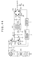
- FIG. 44 shows the switching power supply circuit disclosed in Patent Document 1 and including a resonance type converter.
- the power supply circuit shown includes a switching converter.
- the switching converter is configured such that a partial voltage resonance circuit for performing voltage resonance operation only upon turn-off during switching is combined with a separately excited current resonance type converter of a half bridge coupling scheme.
- the switching power supply circuit shown in FIG. 44 is provided, for example, as a power supply of a printer apparatus.
- the load power exhibits a variation over a comparatively wide range from approximately 100 W or more to no load.
- a common mode noise filter formed from two filter capacitors CL and a common mode choke coil CMC is connected to a commercial AC power supply AC.
- a rectification smoothing circuit for producing a DC input voltage from the commercial AC power supply AC
- a full wave rectification circuit formed from a bridge rectification circuit Di and a smoothing capacitor Ci is provided at the next stage to the common mode noise filter.
- a rectification output of the bridge rectification circuit Di is charged into the smoothing capacitor Ci, and as a result, a rectification smoothed voltage Ei (DC input voltage) having a level equal to that of an AC input voltage VAC is obtained across the smoothing capacitor Ci.
- the current resonance type converter for receiving and switching the DC input voltage includes a switching circuit system wherein two switching devices Q1 and Q2 each formed from a MOS-FET are connected to each other in a half bridge coupling scheme as seen in FIG. 44. Damper diodes DD1 and DD2 each formed from a body diode are individually connected in parallel to each other and in such directions as seen in FIG. 44 between the drain-source of the switching devices Q1 and Q2, respectively.
- a partial resonance capacitor Cp is connected in parallel between the drain-source of the switching device Q2.
- a parallel resonance circuit (partial voltage resonance circuit) is formed from the capacitance of the partial resonance capacitor Cp and the leakage inductance L1 of a primary winding N1. The partial voltage resonance circuit performs partial voltage resonance operation wherein it voltage resonates only upon turning off of the switching devices Q1 and Q2.
- an oscillation and driving circuit 2 formed from, for example, a general-purpose IC is provided.
- the oscillation and driving circuit 2 includes an oscillation circuit and a driving circuit, and applies a driving signal (gate voltage) having a required frequency to the gates of the switching devices Q1 and Q2. Consequently, the switching devices Q1 and Q2 perform switching operation such that they are turned on and off alternately in a required switching frequency.
- An insulating converter transformer PIT Power Isolation Transformer transmits switching outputs of the switching devices Q1 and Q2 to the secondary side.
- the primary winding N1 of the insulating converter transformer PIT is connected at one end thereof to a node (switching output point) between the source of the switching device Q1 and the drain of the switching device Q2 through a primary side series resonance capacitor C1 so that the switching output can be obtained from the node.
- the primary winding N1 is connected at the other end thereof to the primary side ground as seen in FIG. 44.
- the series resonance capacitor C1 and the primary winding N1 are connected in series to each other.
- a primary side series resonance circuit for making operation of the switching converter that of the current resonance type is formed from the capacitance of the series resonance capacitor C1 and the leakage inductance L1 of the primary winding N1 (series resonance winding) of the insulating converter transformer PIT.
- the power supply circuit shown in FIG. 44 adopts a form wherein the resonance circuit for making operation of the primary side switching converter that of the resonance type is combined with another resonance circuit.
- a switching converter of the type just described is hereinafter referred to as composite resonance type converter.
- the insulating converter transformer PIT described above is structured such that it includes an EE type core formed by combining E type cores made of, for example, a ferrite material with each other. Further, the primary winding N1 and a secondary winding N2 are wound on an inner magnetic leg of the EE type core at winding portions provided divisionally for the primary and secondary sides.
- a gap of 1.5 mm or less is formed in the inner magnetic leg of the EE type core of the insulating converter transformer PIT. Consequently, a coupling coefficient of 0.75 or more is obtained between the primary winding N1 and the secondary winding N2.
- a full wave rectification circuit is provided for the secondary winding N2 of the insulating converter transformer PIT.
- the full wave rectification circuit is formed from a bridge rectification circuit formed from rectification diodes Do1 to Do4, and a smoothing capacitor Co.
- a secondary side DC output voltage Eo which is a DC voltage having a level equal to that of the alternating voltage induced in the secondary winding N2, can be obtained as a voltage across the smoothing capacitor Co.
- the secondary side DC output voltage Eo is supplied as main DC power supply to a main load not shown, and is also branched and inputted as a detection voltage for constant voltage control to the control circuit 1.
- the control circuit 1 outputs a control signal in the form of current or a voltage whose level is adjusted corresponding to that of the secondary side DC output voltage Eo to the oscillation and driving circuit 2.
- the frequency of an oscillation signal produced by the oscillation circuit in the oscillation and driving circuit 2 is adjusted based on the control signal inputted from the control circuit 1 to adjust the frequency of the switching driving signal to be applied to the gates of the switching devices Q1 and Q2. Consequently, the switching frequency is adjusted. Since the switching frequency of the switching devices Q1 and Q2 is adjustably controlled in response to the level of the secondary side DC output voltage Eo in this manner, the resonance impedance of the primary side series resonance circuit is varied and also the energy to be transferred from the primary winding N1, which forms the primary side series resonance circuit, to the secondary side is varied. Further, at this time, also the level of the secondary side DC output voltage Eo is adjustably controlled. Consequently, constant voltage control for the secondary side DC output voltage Eo can be implemented.
- switching frequency controlling method for adjustably controlling the switching frequency to achieve stabilization as described above is hereinafter referred to as "switching frequency controlling method".
- the voltage V1 of a rectangular wave is a voltage across the switching device Q2 and indicates on and off timings of the switching device Q2.
- a period that the voltage V1 is the 0 level is an on period that the switching device Q2 conducts.
- switching current IQ2 having a waveform illustrated in FIG. 46 is supplied to the switching circuit system formed from the switching device Q2 and the clamp diode DD2.
- a period that the voltage V1 is clamped with a level of a rectification smoothed voltage Ei is a period that the switching device Q2 is off, and the switching current IQ2 has the zero level as seen in FIG. 46.
- a voltage obtained across the other switching device Q1 and switching current flowing to the switching circuit (Q1, DD1) have waveforms of phases shifted by 180° from those of the waveforms of the voltage V1 and the switching current IQ2, respectively.
- the switching devices Q1 and Q2 perform the switching operation such that they are turned on and off alternately.
- the switching currents flowing to the switching circuits are composed to obtain current having a waveform shown in FIG. 46, and the resulting current is used as primary side series resonance current Io to flow to the primary side series resonance circuit (C1-N1(L1)).
- the switching frequency is controlled.
- the switching frequency decreases in response to decrease of the level of the secondary side DC output voltage Eo as the load becomes heavier, but the switching frequency increases in response to increase of the level of the secondary side DC output voltage Eo as the load becomes lighter. This indicates the fact that constant voltage controlling operation by upper side control is performed as a switching frequency controlling method.
- an alternating voltage V2 having a waveform shown in FIG. 46 is induced in the secondary winding N2 of the insulating converter transformer PIT. Then, within a period of any one of half cycles that the alternating voltage V2 has the positive polarity, the rectification diodes [Do1, Do4] on the secondary side conduct to allow rectification current ID1 to flow in a waveform and at a timing shown in FIG. 46. Further, within a period of the other one of half cycles that the alternating voltage V2 has the negative polarity, the rectification diodes [Do2, Do3] on the secondary side conduct to allow rectification current ID3 to flow in a waveform and at a timing shown in FIG. 46. Further, as seen in FIG. 46, the rectification currents ID1 and ID3 are composed to form secondary winding current I2 to flow to the secondary winding N2.
- the switching frequency fs has a characteristic that it decreases as the load increases because the constant voltage controlling operation is performed.
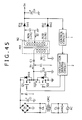
- FIG. 45 Another example of the switching power supply circuit is shown in a circuit diagram of FIG. 45. It is to be noted that, in FIG. 45, like elements to those of FIG. 44 are denoted by like reference characters, and description of them is omitted herein to avoid redundancy.
- the secondary side rectification circuit of the power supply circuit shown in FIG. 45 includes a full wave rectification circuit.
- a center tap is provided for the secondary winding N2 such that the secondary winding N2 is divided into secondary winding sections N2A and N2B.
- the secondary winding sections N2A and N2B are formed from numbers of turns equal to each other.
- the center tap is grounded to the secondary side ground.
- the rectification diodes Do1 and Do2 and the secondary side smoothing capacitor Co are connected to the secondary winding N2.
- the full wave rectification circuit the secondary side DC output voltage Eo can be obtained as a voltage across the smoothing capacitor Co.
- the power supply circuit having such a configuration as described above is provided as a power supply of a plasma display apparatus.
- the power supply circuit shown in FIG. 45 is provided as a power supply of a plasma display apparatus and is configured so that the secondary side DC output voltage Eo obtained has a comparatively high level.
- the secondary side rectification circuit is formed as a full wave rectification circuit, and the number of turns of the secondary winding N2 is suitably increased to 100 T.
- the adjustable controlling range of the switching frequency for stabilization is a comparatively wide range.
- FIG. 48 illustrates a constant voltage controlling characteristic of the power supply circuit shown in FIG. 44 (FIG. 45) in the form of a relationship between the level of the switching frequency fs and the level of the secondary side DC output voltage Eo.
- the upper side control herein is a controlling method for adjustably controlling the switching frequency within a frequency range higher than a resonance frequency fo1 of the primary side series resonance circuit and utilizing the variation of the resonance impedance caused by the adjustment control to control the level of the secondary side DC output voltage Eo.
- the resonance impedance of the series resonance circuit is lowest at the resonance frequency fo1. Consequently, as a relationship between the secondary side DC output voltage Eo and the switching frequency fs in the upper side control, the level of the secondary DC output voltage Eo increases as the switching frequency fs approaches the resonance frequency fo1, but decreases as the switching frequency fs is spaced away from the resonance frequency fo1.
- the level of the secondary side DC output voltage Eo with respect to the switching frequency fs in a condition that the load power Po is constant exhibits a quadratic curve variation.
- the level of the secondary side DC output voltage Eo exhibits a peak when the switching frequency fs is equal to the resonance frequency fo1 of the primary side series resonance circuit, and decreases as the switching frequency fs is spaced away from the resonance frequency fo1.
- the level of the secondary side DC output voltage Eo corresponding to the switching frequency fs in a condition same as that described above exhibits a characteristic that it shifts such that the level at the maximum load power Pomax decreases by a predetermined amount with respect to the level at the minimum load power Pomin.
- the level of the secondary side DC output voltage Eo decreases as the load condition becomes heavier.
- the adjustment range (necessary control range) of the switching frequency necessary for the power supply circuit shown in FIG. 44 is a range indicated by reference character ⁇ fs.
- the power supply circuit shown in FIG. 44 performs the constant voltage control based on the switching frequency controlling method so that the secondary side DC output voltage Eo is stabilized at 135 V so as to cope with the input variation range and the load conditions.
- the power supply circuit shown in FIG. 45 performs the constant voltage control so that the secondary side DC output voltage Eo is stabilized at the rated level of approximately 200 V. Therefore, similarly as in the power supply circuit shown in FIG. 44, the range ⁇ fs of the power supply circuit shown in FIG. 45 is a correspondingly wide range.
- a power supply circuit ready for a wide range is known, which is configured so as to operate with an AC input voltage range, for example, from approximately AC 85 V to 288 V. It can be applied in both of an area in which the AC input voltage of the AC 100 V type is applied such as, for example, Japan, U.S.A. and so forth and another area in which the AC input voltage of the AC 200 V type is applied such as, for example, Europe.
- the power supply circuit shown in FIG. 44 (FIG. 45) is configured as a power supply circuit ready for a wide range described above.
- the power supply circuit ready for a wide range, it is ready for the AC input voltage range, for example, from AC 85 V to 288 V. Accordingly, also the variation range of the level of the secondary side DC output voltage Eo increases when compared with that in an alternative case wherein the power supply circuit is ready for a single range of, for example, only the AC 100 V type or only the AC 200 V type.
- switching frequency control over a still wider range is required. For example, in the power supply circuit shown in FIG. 44 (FIG. 45), it is necessary to expand the controlling range of the switching frequency fs to approximately 80 kHz to 500 kHz.
- the upper limit to the driving frequency with which an IC (oscillation driving circuit 2) for driving an actual switching device can cope is approximately 200 kHz. Further, even if a switching driving IC that can be driven with such a high frequency as described above is configured and mounted, when the switching device is driven with such a high frequency as described above, the power conversion efficiency drops remarkably. Therefore, it is difficult to practically use the switching driving IC described above as an actual power supply circuit.
- the upper limit to the AC input voltage VAC which can be stabilized, for example, by the power supply circuit shown in FIG. 44 (FIG. 45), is approximately 100 V.
- a rectification circuit system receiving a commercial AC power supply to produce the DC input voltage (Ei) is provided with a function of performing changeover between a voltage doubler rectification circuit and a full wave rectification circuit in response to an input of commercial AC power supply of the AC 100 V type and the AC 200 V type.
- the circuit is configured such that the level of the commercial AC power supply is detected and the circuit connection of the rectification circuit system is changed over by a switch using an electromagnetic relay such that a voltage doubler rectification circuit or a full wave rectification circuit is formed in response to the detected level.
- the DC input voltage of the converter on the standby power supply side is detected in order to prevent a malfunction. It signifies that only an electronic apparatus including not only a main power supply but also a standby power supply can actually use a power supply circuit including a circuit for changing over rectification operation and being ready for a wide range. In other words, the type of an electronic apparatus in which the power supply can be incorporated is limited to that including a standby power supply, and the range of utilization becomes narrower as much.
- any one of the configurations described above is adopted as a configuration ready for a wide range in such a manner as described above, when compared with an alternative configuration ready for a single range, increase of the circuit scale and increase of the cost caused by increase of the number of parts cannot be avoided. Further, intrinsic problems, which do not appear with the configuration ready for a single range, such as a limitation to the utilization range of an apparatus and increase of switching noise and so forth occur with the former configuration and the latter configuration, respectively.
- control range of the switching frequency is a suitably wide range as in the case of the power supply circuit as shown in FIG. 44 (FIG. 45)
- a problem occurs that a highspeed response characteristic in stabilization of the secondary side DC output voltage Eo decreases.
- Some electronic apparatus involves operation varying such that the load condition changed over instantaneously, for example, between a state wherein the load has a maximum level and another state wherein the load is substantially zero.
- a load exhibiting such a load variation as just described is also called switching load.
- the power supply circuit to be incorporated in such an apparatus as just described must be configured so that the secondary side DC output voltage is appropriately stabilized against the load variation such as that of the switching load.
- a switching power supply circuit including switching means, switching driving means, the insulating converter transformer, a primary side series resonance circuit, a secondary side series resonance circuit, secondary side DC output voltage production means, constant voltage control means, and composite coupling coefficient setting means.
- the switching means includes a switching device for receiving a DC input voltage as an input thereto to perform switching.
- the switching driving means drives the switching device for switching.
- the insulating converter transformer is wound with at least a primary winding to which a switching output obtained by the switching operation of the switching means is supplied and a secondary winding in which an alternating voltage is induced by the primary winding.
- the insulating converter transformer has a gap formed at a predetermined position of a core thereof and has a gap length set so that a predetermined coupling coefficient may be obtained between the primary side and secondary side.
- the primary side series resonance circuit is formed at least from a leakage inductance component of the primary winding of the insulating converter transformer and a capacitance of a primary side series resonance capacitor connected in series to the primary winding so that a predetermined resonance frequency may be set for making operation of the switching means that of a current resonance type.
- the secondary side series resonance circuit is formed at least from a leakage inductance component of the secondary winding of the insulating converter transformer and a capacitance of a secondary side series resonance capacitor connected in series to the secondary winding so that at least a predetermined resonance frequency may be set.
- the secondary side DC output voltage production means receives a resonance output obtained by the secondary side series resonance circuit as an input thereto and performs rectification operation for the inputted resonance output to produce a secondary side DC output voltage.
- the constant voltage control means controls the switching driving means in response to a level of the secondary side DC output voltage to adjust a switching frequency of the switching means to perform constant voltage control for the secondary side DC output voltage.
- the composite coupling coefficient setting means sets the composite coupling coefficient between the primary side and the secondary side of the insulating converter transformer so that an output characteristic of an electromagnetic coupling type resonance circuit formed from the primary side series resonance circuit and the secondary side series resonance circuit with respect to an input of a frequency signal having the switching frequency may become a unimodal characteristic.
- the switching power supply circuit adopts a basic configuration as a current resonance type converter including a primary side series resonance circuit and forms a series resonance circuit formed also on the secondary side from a secondary winding and a secondary side series resonance capacitor.
- the switching power supply circuit of the present invention includes a coupling type resonance capacity formed by the magnetic coupling of the insulating converter transformer. Further, the composite coupling coefficient between the primary side and the secondary side of the insulating converter transformer in the power supply circuit is set to a value with which a steep unimodal characteristic is obtained as an output characteristic with respect to a frequency signal (switching output) of the switching frequency, which is an input to the coupling type resonance circuit. Since the unimodal characteristic is obtained in this manner, the variation range or necessary control range of the switching frequency required for stabilization can be reduced when compared with an alternative case wherein a series resonance circuit is formed only on the primary side.
- variable control range that is, the necessary control range, of the switching frequency necessary for the constant voltage control is reduced.
- the responsibility of the constant voltage control is improved. This makes it possible to perform constant voltage control with a higher responsibility than ever for a load variation called switching load which varies in a switching manner between a maximum load condition and a no-load condition. This enhances the reliability of an apparatus in which the switching power supply circuit is incorporated.
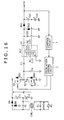
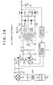
- FIG. 1 shows an example of a configuration of a switching power supply circuit according to a first embodiment of the present invention.
- the power supply circuit is configured such that the basic configuration of the primary side thereof is a combination of a partial voltage resonance circuit with a separated excited current resonance type converter of a half-bridge coupling type.
- the power supply circuit of the first embodiment has a configuration ready for a wide range.
- the circuit operates in response to both of commercial AC power supplies of the AC 100 V type and the AC 200 V type.
- the power supply circuit is supposed to be used as a power supply, for example, of a printer apparatus and is configured so as to be ready for the load power Po from 150 W to 0 W.
- a common mode noise filter is provided for a commercial AC power supply AC and formed from a pair of filter capacitors CL and a common mode choke coil CMC.
- a full-wave rectification circuit including a bridge rectification circuit Di and a smoothing capacitor Ci is connected to the commercial AC power supply AC at the following stage of the noise filter.
- the full-wave rectification circuit receives the commercial AC power supply AC to perform full-wave rectification operation such that a rectification smoothed voltage Ei (DC input voltage) is obtained across the smoothing capacitor Ci.
- the rectification smoothed voltage Ei in this instance has a voltage level equal to that of an AC input voltage VAC.
- a current resonance type converter for receiving and switching (interrupting) the DC input voltage includes a switching circuit formed from two switching elements Q1 and Q2 each in the form of a MOS-FET connected in a half-bridge connection as seen in FIG. 1.
- Damper diodes DD1 and DD2 are connected in parallel between the drain-source of the switching elements Q1 and Q2, respectively.
- the anode and the cathode of the damper diode DD1 are connected to the source and the drain of the switching element Q1, respectively.
- the anode and the cathode of the damper diode DD2 are connected to the source and the drain of the switching element Q2, respectively.
- the damper diodes DD1 and DD2 are provided as body diodes for the switching elements Q1 and Q2, respectively.
- a primary side partial resonance capacitor Cp is connected in parallel between the drain-source of the switching element Q2.
- the capacitance of the primary side partial resonance capacitor Cp and the leakage inductance L1 of a primary winding N1 cooperatively form a parallel resonance circuit (partial voltage resonance circuit). Partial voltage resonance operation that the switching elements Q1 and Q2 exhibit voltage resonance only upon turning off of the switching elements Q1 and Q2 is obtained.
- An oscillation driving circuit 2 is provided to drive the switching elements Q1 and Q2 for switching.
- the oscillation driving circuit 2 includes an oscillation circuit and a driving circuit and may be formed, for example, using an IC for universal use.
- the oscillation circuit of the oscillation driving circuit 2 generates an oscillation signal of a required frequency, and the driving circuit makes use of the oscillation signal to generate a switching driving signal used as a gate voltage for driving a MOS-FET for switching.
- the switching driving signal is applied to the gates of the switching elements Q1 and Q2. Consequently, the switching elements Q1 and Q2 successively and alternately turn on and off in accordance with a switching frequency corresponding to the period of the switching driving signal to perform switching operation.
- An insulating converter transformer PIT is provided to transmit the switching outputs of the switching elements Q1 and Q2 to the secondary side.
- the insulating converter transformer PIT has the primary winding N1.
- the primary winding N1 is connected at one end thereof to a node (switching output point) between the source of the switching element Q1 and the drain of the switching element Q2 through a series connection of a primary side series resonance capacitor C1 so that the switching outputs are transmitted.
- the primary winding N1 is connected at the other end thereof to the primary side ground.
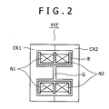
- the insulating converter transformer PIT has such a structure as shown in a sectional view of FIG. 2.
- the insulating converter transformer PIT includes an EE type core (EE-shaped core) formed from a pair of E-type cores CR1 and CR2 made of a ferrite material and combined with each other such that magnetic legs thereof are opposed to each other.
- EE type core EE-shaped core
- the insulating converter transformer PIT further includes a bobbin B made of, for example, a resin material and having such a divisional shape such that winding receiving portions on the primary side and the secondary side thereof are independent of each other.
- the primary winding N1 is wound on one of the winding receiving portions of the bobbin B.
- a secondary winding N2 is wound on the other winding receiving portion.
- the bobbin B on which the primary winding N1 and the secondary winding N2 are wound in this manner is attached to the EE type core (CR1, CR2). Consequently, the primary side winding and the secondary side winding are wound in the different winding regions on the inner magnetic leg of the EE type core.
- the structure of the insulating converter transformer PIT as a whole is obtained.
- a gap G is formed in such a manner as seen in FIG. 2 in the inner magnetic leg of the EE type core.
- the gap G can be formed by forming the inner magnetic leg of each of the E-type cores CR1 and CR2 shorter than the other two outer magnetic legs.
- the gap formed in the core of the insulating converter transformer PIT is set, for example, to 1.5 mm to 1.6 mm or less so as to obtain the coupling coefficient k of 0.75 or more.
- the coupling degree between the primary side and the secondary side of the insulating converter transformer PIT is set further lower than those in the power supply circuits in related art.
- the primary winding N1 has a predetermined leakage inductance L1. Further, as described hereinabove, the primary winding N1 and the primary side series resonance capacitor C1 are connected in series. Accordingly, the leakage inductance L1, of the primary winding N1, and the capacitance of the primary side series resonance capacitor C1 cooperatively form a series resonance circuit (primary side series resonance circuit).
- the primary side series resonance circuit is connected to the switching output point of the switching elements Q1 and Q2. Consequently, the switching output of the switching elements Q1 and Q2 is transmitted to the primary side series resonance circuit.
- the primary side series resonance circuit performs resonance operation with the switching output transmitted thereto thereby to make the operation of the primary side switching converter that of the current resonance type.
- the primary side switching converter shown in FIG. 1 performs operation as that of the current resonance type by the primary side series resonance circuit (L1-C1) and partial voltage resonance operation by the primary side partial voltage resonance circuit (Cp//L1) described hereinabove.
- the primary side of the power supply circuit shown in FIG. 1 has a configuration as follows.
- a resonance circuit for making the primary side switching converter that of the resonance type is combined with another resonance circuit.
- a switching converter formed from a combination of two resonance circuit in this manner is hereinafter referred to as "composite resonance type converter”.
- a secondary side series resonance capacitor C2 is connected in series to one end portion of the secondary winding N2. Consequently, a secondary side series resonance circuit is formed from the capacitance of the secondary side series resonance capacitor C2 and a leakage inductance L2 of the secondary winding N2.
- a series resonance circuit is formed on each of the primary and secondary sides of the insulating converter transformer PIT.
- a full-wave rectification circuit is connected to the secondary side series resonance circuit (L2-C2).
- the full-wave rectification circuit is formed from a bridge rectification circuit formed from four rectification diodes Do1 to Do4 connected in such a manner as seen in FIG. 1, and a smoothing capacitor Co.
- the full rectification circuit operates such that, within one of two half periods of an alternating voltage excited in the secondary winding N2, the set of the rectification diodes [Do1, Do4] of the bridge rectification circuit conduct to charge the rectification current into the smoothing capacitor Co. On the other hand, within the other half period of the alternating voltage excited in the secondary winding N2, the other set of the rectification diodes [Do2, Do3] conduct to charge the rectification current into the smoothing capacitor Co.
- a secondary side DC output voltage Eo obtained as a voltage across the smoothing capacitor Co has a level equal to the level of the alternating voltage excited in the secondary winding N2.
- the secondary side DC output voltage Eo obtained in this manner is supplied to a load not shown and also is branched and inputted as a detection voltage for a control circuit 1 hereinafter described.
- the full wave rectification circuit performs rectification smoothing operation for the resonance output of the secondary side series resonance circuit
- the secondary side rectification operation of the full wave rectification circuit is that of the current resonance type.
- the rectification current waveform includes a sine waveform of the resonance frequency of the secondary side series resonance circuit.
- the relationship between the resonance frequency fo1 of the primary side series resonance circuit and the resonance frequency fo2 of the secondary side series resonance circuit is set such that the resonance frequency fo2 is lower than the resonance frequency fo1.
- the resonance frequency fo1 is set to approximately 70 kHz while the resonance frequency fo2 is set to approximately 35 kHz so as to be approximately 1/2 the resonance frequency fo1.
- a secondary side partial resonance capacitor Cp2 is inserted in parallel to the series connection circuit of the secondary winding N2 and the secondary side series resonance capacitor C2 which form the secondary side series resonance circuit (L2-C2).
- the capacitance of the secondary side partial resonance capacitor Cp2 and the leakage inductance L2 of the secondary winding N2 cooperatively form a parallel resonance circuit as a secondary side partial voltage resonance circuit (partial resonance circuit).
- the secondary side partial voltage resonance circuit performs secondary side partial voltage resonance operation.
- the secondary side partial voltage resonance operation voltage resonates only at timings at which the set of the rectification diodes [Do1 to Do4] and the other set of the rectification diodes [Do2, Do3], which form the secondary side full-wave rectification circuit, turn off and on.
- the partial voltage resonance operation forms a path along which reverse current produced when each of the sets of the rectification diodes [Do1, Do4] and [Do2, Do3] turns off. Since the reactive power at this time decreases, reduction of the power loss by the secondary side rectification circuit is achieved.
- the switching power supply circuit of the present invention includes a primary side series resonance circuit (L1-C1) and a primary side partial voltage resonance circuit (L1//Cp) on the primary side and includes a secondary side series resonance circuit (L2-C2) and a secondary side partial voltage resonance circuit (L2//Cp2) on the secondary side.
- L1-C1 primary side series resonance circuit
- L1//Cp primary side partial voltage resonance circuit
- L2-C2 secondary side series resonance circuit
- L2//Cp2 secondary side partial voltage resonance circuit
- a switching converter including a combination of two resonance circuits which includes a series resonance circuit and a partial voltage resonance circuit like those on the secondary side, is hereinafter referred to as composite resonance type converter.
- a switching converter including a combination of three or more resonance circuits as in the case of the present embodiment is hereinafter referred to as multiple (composite) resonance type converter.
- the control circuit 1 is provided to stabilize the secondary side DC output voltage Eo in accordance with a switching frequency controlling method.
- the control circuit 1 in this instance supplies a detection output corresponding to a level variation of the secondary side DC output voltage Eo, which is a detection input, to the oscillation driving circuit 2.
- the oscillation driving circuit 2 drives the switching elements Q1 and Q2 so as to vary the switching frequency in response to the detection output of the control circuit 1 inputted thereto. To this end, the oscillation driving circuit 2 varies the frequency of the oscillation signal to be produced by the internal oscillation circuit.
- the switching frequency of the switching elements Q1 and Q2 varies, the resonance impedance of the primary side series resonance circuit, and the power amount to be transmitted from the primary winding N1 to the secondary winding N2 side of the insulating converter transformer PIT varies thereby to stabilize the level of the secondary side DC output voltage Eo.
- a frequency range higher than an intermediate resonance frequency fo is set as a variation range of the switching frequency.
- the intermediate resonance frequency fo depends upon the resonance frequency fo1 of the primary side series resonance circuit and the resonance frequency fo2 of the secondary side series resonance circuit. In other words, an upper side controlling system is adopted.
- a series resonance circuit exhibits the lowest resonance impedance at its resonance frequency. From this, where the upper side controlling system based on the resonance frequency of a series resonance circuit is adopted as in the present embodiment, the resonance impedance is increases as the switching frequency fs increases.
- the switching frequency is controlled so as to become lower. This decreases the resonance impedance and increases the power transmission amount from the primary side to the secondary side, and consequently, the secondary side DC output voltage Eo rises.
- the switching frequency is controlled so as to become higher. Consequently, the resonance impedance increases and the power transmission amount described above decreases. Consequently, the secondary side DC output voltage Eo drops.
- the switching frequency is varied in this manner to stabilize the secondary side DC output voltage Eo.
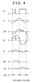
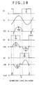
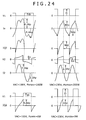
- FIGS. 3 and 4 illustrate operation waveforms of the components of the power supply circuit shown in FIG. 1.
- the core of the EER type is included in one of types or standards of the core as a product as well known in the art, and also it is known that the EER type includes the EE type.
- the term EE type is used to include both of the EER type and the EE type because the cores of the both type have a EE-shaped cross section.
- the voltage V1 is a voltage across the switching element Q2 and indicates on/off timings of the switching element Q2.
- the switching current IQ2 of the switching element Q2 illustrated in FIGS. 3 and 4 flows and the switching element Q2 exhibits an on state.
- the switching current IQ2 has the zero level and the switching element Q2 exhibits an off state.
- the voltage across the switching element Q1 has a waveform shifted by 180 degrees from that of the voltage V1.
- the switching current IQ1 of the switching element Q1 has a waveform having a phase shifted by 180 degrees from that of the switching current IQ2.
- the switching element Q1 and the switching element Q2 are switched on and off alternately.
- the primary side series resonance current Io flowing through the primary side series resonance circuit has such a waveform as seen in FIGS. 3 and 4.
- the waveform is a composite waveform of the switching current IQ1 and the switching current IQ2.
- the period of the waveforms of FIG. 4 is shorter than that of the waveforms of FIG. 3.
- the voltage V1 and the switching current IQ2 are controlled so that the switching frequency increases as the load decreases from a high load to a low load.
- the stabilization control is performed such that, where the load becomes heavier and the level of the secondary side DC output voltage Eo decrease, the switching frequency is decreased, but where the load becomes lighter and the level of the secondary side DC output voltage Eo increases, the switching frequency is increased.
- the peak level of the switching current IQ2 is 4 Ap as seen in FIG. 3.
- the peak level of the switching current IQ2 is 2 Ap. From this, it can be recognized also that the switching current on the primary side is changed so as to increase in response to a decreasing tendency of the level of the secondary side DC output voltage Eo in a heavy load condition, but the switching current is changed to decrease in response to an increasing tendency of the level of the secondary side DC output voltage Eo in a light load condition.
- an alternating voltage V2 illustrated in FIG. 3 or 4 flows through the secondary winding N2 of the insulating converter transformer PIT.
- the positive and negative peak levels (absolute values) of the alternating voltage V2 are equal to the level of the secondary side DC output voltage Eo.
- the rectification current ID1 in which the rectification diodes [Do1 to Do4] conduct and flow, flows within a period that the alternating voltage V2 excited in the secondary winding N2 has the positive polarity as seen in FIGS. 3 and 4.
- the rectification current ID3 in which the rectification diodes [Do2, Do3] conduct and flow, flows within another period that the alternating voltage V2 has the negative polarity.
- the rectification current I2 is obtained at a line between the secondary side ground and the node of the rectification diodes Do2 and Do4 serving as a negative output terminal of the bridge rectification circuit, and has such a waveform as seen in FIG. 3 or 4.
- the waveform is a composite waveform of the rectification currents ID1 and ID3.
- the current ICp2 flows through the secondary side partial resonance capacitor Cp2 provided on the secondary side. As seen in FIG. 3 or 4, the current ICp2 flows at timings at which the rectification diodes Do1 to Do4 are turned off. In particular, it can be seen from the waveform of the current ICp2 that reverse current generated upon turning off of the rectification diodes Do1 to Do4 flows. Also by this, suppression of the power loss of the rectification diodes Do1 to Do4 can be achieved as described hereinabove.
- the power supply circuit of FIG. 1 having the configuration described above includes series resonance circuits (primary side series resonance circuit (L1-C1) and secondary side series resonance circuit (L2-C2)) individually on the primary side and the secondary side.
- series resonance circuits primary side series resonance circuit (L1-C1) and secondary side series resonance circuit (L2-C2)
- L1-C1-C1-C1-C2 secondary side series resonance circuit
- L2-C2 secondary side series resonance circuit
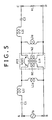
- FIG. 5 shows an equivalent circuit where the power supply circuit of the present embodiment shown in FIG. 1 is viewed from a relationship between the primary side series resonance circuit and the secondary side series resonance circuit.
- the primary winding N1 and the secondary winding N2 wound thereon have predetermined numbers of turns such that they have a winding turn ratio of 1:n. Further, it is shown that the coupling degree between the primary side and the secondary side of the insulating converter transformer PIT is given by the coupling coefficient k.
- the primary winding N1 has a leakage inductance L1l and has an exciting inductance L1e.
- the secondary winding N2 has a leakage inductance L2l and an exciting inductance L2e.
- alternating current (frequency signal) of the switching frequency fs is inputted to the primary side of the insulating converter transformer PIT.
- switching output of the primary side switching converter is inputted to the primary side of the insulating converter transformer PIT.
- the primary side series resonance circuit can be regarded as a circuit wherein the series circuit of the primary side series resonance capacitor C1 and the leakage inductance L1l is connected in series to the primary winding N1 and the exciting inductance L1e is connected in parallel to the primary winding N1.
- the secondary side series resonance circuit of the insulating converter transformer PIT can be regarded as a circuit wherein the series circuit of the secondary side series resonance capacitor C2 and the leakage inductance L21 is connected in series to the secondary winding N2 and the exciting inductance L2e is connected in parallel to the secondary winding N2 similarly. Further, in FIG. 5, the output of the secondary side series resonance circuit is outputted to a load RL.
- the load RL is circuits and a load which are connected following the secondary side full wave rectification circuit.
- the equivalent circuit includes a primary side series resonance circuit on the primary side and a secondary side series resonance circuit on the secondary side through electromagnetic induction of the insulating converter transformer PIT. Accordingly, the circuit shown in FIG. 5 can be considered such that it forms a coupling type resonance circuit by electromagnetic coupling. Therefore, the constant voltage control characteristic for the secondary side DC output voltage Eo in the power supply circuit shown in FIG. 1 varies depending upon the coupling degree (coupling coefficient k) of the insulating converter transformer PIT. This is described more particularly with reference to FIG. 6.
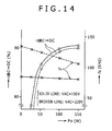
- FIG. 6 illustrates an output characteristic of the equivalent circuit of FIG. 5 with respect to an input (switching frequency signal) thereto.
- FIG. 6 illustrates the control characteristic of the secondary side DC output voltage Eo in relation to the switching frequency fs.
- the axis of abscissa indicates the switching frequency
- the axis of ordinate indicates the level of the secondary side DC output voltage Eo.
- the resonance frequency fo1 of the primary side series resonance circuit and the resonance frequency fo2 of the secondary side series resonance circuit have the relationship of fo1 > fo2. While, in FIG. 6, the resonance frequencies fo1 and fo2 are illustrated with respect to the axis of abscissa indicating the switching frequency fs, where fo1 > fo2 as in the case of the circuit of FIG. 1, it is illustrated that the resonance frequency fo2 is lower than the resonance frequency fo1. On the other hand, if fo1 ⁇ fo2 conversely, then it is illustrated that the resonance frequency fo2 is higher than the resonance frequency fo1.
- the constant voltage control characteristic is a bimodal characteristic.
- the secondary side DC output voltage Eo has peaks at frequencies f1 and f2 different from the resonance frequency fo1 and the resonance frequency fo2 as seen from a characteristic curve 1 in FIG. 6.
- fo which is one of the terms, is an intermediate frequency between the resonance frequency fo1 of the primary side series resonance circuit and the resonance frequency fo2 of the secondary side series resonance circuit and depends upon an impedance of the primary side, an impedance of the secondary side, and an impedance (mutual coupling inductance M) common to the primary side and the secondary side.
- a unimodal characteristic is obtained as seen from a further characteristic curve 3 in FIG. 6.
- the unimodal characteristic indicates that the secondary side DC output voltage Eo has a peak only at the intermediate resonance frequency fo. If the characteristic curve 3 is compared with the characteristic curves 1 and 2, then it can be recognized that the peak level itself of the characteristic curve 3 is lower than those of the characteristic curved 1 and 2. However, the characteristic curve 3 has a steeper inclination as a curved shape like a quadratic function.
- the insulating converter transformer PIT in the present embodiment has a loose coupling setting wherein the coupling coefficient k is k ⁇ 0.65. According to the setting of the coupling coefficient k, the secondary side DC output voltage Eo operates with the unimodal characteristic indicated by the characteristic curve 3.
- the unimodal characteristic illustrated in FIG. 6 and the constant voltage control characteristic of the composite resonance type converter of the power supply circuit in related art (FIG. 44 or 45) described hereinabove with reference to FIG. 48 are actually compared with each other. It can be seen that, when compared with the characteristic illustrated in FIG. 6, the characteristic illustrated in FIG. 48 exhibits a considerably moderate inclination as a quadratic function.
- the constant voltage control characteristic of the present embodiment is such as illustrated in FIG. 7 because it has a unimodal characteristic indicated by the characteristic curve 3 in FIG. 6.
- characteristic curves A, B, C, and D are illustrated including characteristic curves A, B, C, and D.
- the variation control range ⁇ fs1 is a frequency range from the switching frequency fs at which the characteristic curve A exhibits the level tg to the switching frequency fs at which the characteristic curve B exhibits the level tg.
- the variation control range ⁇ fs2 is a frequency range from the switching frequency fs at which the characteristic curve C exhibits the level tg to the switching frequency fs at which the characteristic curve D exhibits the level tg.
- the unimodal characteristic which is a control characteristic of the secondary side DC output voltage Eo in the present embodiment, is considerably steep as a curve of a quadratic function when compared with the control characteristic described hereinabove with reference to FIG. 48.
- the frequency variation range ( ⁇ fsA) from the lowest switching frequency (switching frequency fs at which the characteristic curve A exhibits the level tg) of the variation control range ⁇ fs1 to the highest switching frequency (switching frequency fs at which the characteristic curve A exhibits the level tg) of the variation control range ⁇ fs2 becomes narrower correspondingly.
- the actual frequency variation range ⁇ fsA of the power supply circuit of the present embodiment shown in FIG. 1 sufficiently falls within the variation range of the switching frequency for which a switching driving IC (oscillation driving circuit 2) at present can be ready.
- the power supply circuit of FIG. 1 can variably control the switching frequency actually with the frequency variation range ⁇ fsA. This signifies that the power supply circuit shown in FIG. 1 can be ready for a commercial AC power supply input of both of the AC 100 V type and the AC 200 V type to stabilize the secondary side DC output voltage Eo. In other words, the power supply circuit shown in FIG. 1 can be ready for a wide range only by switching frequency control.
- a coupling type resonance circuit by electromagnetic coupling is already known as a technique for expanding the amplification bandwidth of an amplification circuit by transistors in communication techniques such as, for example, an intermediate frequency transformer amplifier.
- communication techniques such as, for example, an intermediate frequency transformer amplifier.
- a bimodal characteristic by a close coupling or a flat characteristic by a critical coupling is used, and a unimodal characteristic by a loose coupling is not used.
- the present embodiment utilizes a unimodal characteristic by a loose coupling, which has not been adopted in the field of communication techniques, with regard to a technique of such a coupling type resonance circuit as described above by an electromagnetic coupling positively in the field of resonance type switching converters.
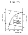
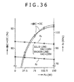
- FIG. 8 illustrates characteristics of the power supply circuit shown in FIG. 1 and particularly illustrates an AC ⁇ DC power conversion efficiency and a switching frequency control characteristic with respect to a load variation.
- the characteristic of the switching frequency fs exhibits a variation reduced from that of the circuit in related art described hereinabove with reference to FIG. 44 or 45.
- the variation of the switching frequency fs with respect to a variation of the load power Po within a range from a light load condition to a no load condition is suppressed significantly.
- the necessary control range ⁇ fsA over the range of the commercial AC power supply of the AC 100 V type to the AC 200 V type is approximately 80 to 160 kHz. This sufficiently remains within the frequency variation range (approximately 50 to 200 kHz) of the switching driving IC (oscillation driving circuit 2) at present described hereinabove, and from this, it can be understood that an existing IC can be used as it is for the implementation of the configuration ready for a wide range according to the present embodiment.
- G approximately 1.5 mm
- the power supply circuit of the present embodiment shown in FIG. 1 makes it possible to be ready for a wide range only by switching frequency control.
- a secondary side series resonance capacity it is necessary for only one part of a secondary side series resonance capacity to be added as a necessary but minimum part to the configuration of current resonance type converters in related art including a series resonance circuit only on the primary side.
- a power supply circuit ready for a wide range can be implemented by addition of a number of parts much smaller than that of a configuration in related art according to a circuit changeover system.
- some electronic apparatus performs such operation called switching load operation.
- the load power Po varies in such a manner as to switch or change over at a comparatively high speed between a maximum load condition and a no load condition.
- printers and plasma display apparatus which are peripheral apparatus of personal computers, are listed as apparatus performing such switching load operation.
- the power supply circuit of the first embodiment is configured intending that it can be incorporated as a power supply for a printer.
- the necessary control range ⁇ fs is reduced significantly particularly within a region for a single range, it is possible to stabilize the secondary side DC output voltage Eo at a high speed in response to a steep variation of the load power Po between a maximum load condition and a no load condition. In short, the responding performance of constant voltage control for a switching load is improved significantly.
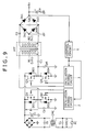
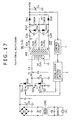
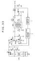
- FIG. 9 shows an example of a configuration of a power supply circuit according to a first modification to the first embodiment described above.
- the modified power supply circuit shown in FIG. 9 naturally has a basic configuration similar to that of the first embodiment and includes principal components selectively set similarly to those of the power supply circuit of FIG. 1. Consequently, in the modified power supply circuit, the coupling coefficient k of the insulating converter transformer PIT and the resonance frequencies fo1 and fo2 are set similar to those in the power supply circuit of the first embodiment.
- the power supply circuit of FIG. 9 has a configuration for being ready for a heavier load condition.
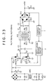
- the power supply circuit shown includes a primary side current resonance type converter including four switching elements Q1 to Q4 connected in a full bridge connection.
- a half bridge connection of the switching elements Q1 and Q2 and another half bridge connection of the switching elements Q3 and Q4 are connected in parallel to each other.
- damper diodes DD3 and DD4 each in the form of a body diode are connected in parallel between the drain-source of them, respectively, similarly to the switching elements Q1 and Q2.
- the primary side series resonance circuit formed from a series connection of the primary winding N1 of the insulating converter transformer PIT and the primary side series resonance capacitor C1 is connected in the following manner.
- one end (winding ending end portion) of the primary winding N1 which is one of end portions of the primary side series resonance circuit, is connected to a node between the source of the switching element Q1 and the drain of the switching element Q2.
- the node between the source of the switching element Q1 and the drain of the switching element Q2 is set as one of switching output points of the switching circuit system of the full bridge connection.
- the other end portion (winding starting end portion) of the primary winding N1 is connected to a node between the source of the switching element Q3 and the drain of the switching element Q4, which is set as the other switching output point, through a series connection of the primary side series resonance capacitor C1.
- the primary side partial resonance capacitor Cp1 is connected in parallel between the source-drain of the switching element Q4.
- the capacitance also of the primary side partial resonance capacitor Cp1 cooperates with the leakage inductance L1 of the primary winding N1 (and the inductance of a high frequency inductor L11) to form a parallel resonance circuit (partial voltage resonance circuit).
- the capacitor Cp1 obtains partial voltage resonance operation that voltage resonates only upon turning off of the switching elements Q3 and Q4.
- the oscillation driving circuit 2 drives the switching elements Q1 and Q2 so as to turn on/off alternately while the oscillation driving circuit 3 drives the switching elements Q3 and Q4 so as to turn on/off alternately. Further, the oscillation driving circuits 2 and 3 generally perform switching driving such that the set of the switching elements [Q1, Q4] and the set of the switching elements [Q3, Q4] turn on/off alternately.
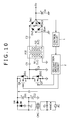
- FIG. 10 shows an example of a configuration of a power supply circuit according to a second modification to the first embodiment described above. Also the modified power supply circuit shown in FIG. 10 naturally has a basic configuration similar to that of the first embodiment and has a configuration for being ready for a heavier load condition.
- the modified power supply circuit includes, as a rectification current circuit system for receiving a commercial AC power supply AC (AC input voltage VAC) as an input thereto to produce a rectification smoothed voltage Ei (DC input voltage), a voltage doubler rectification circuit for producing the rectification smoothed voltage Ei of a level equal to twice that of the AC input voltage VAC.
- AC input voltage VAC AC input voltage
- VAC DC input voltage
- a voltage doubler rectification circuit for producing the rectification smoothed voltage Ei of a level equal to twice that of the AC input voltage VAC.
- the voltage doubler rectification circuit includes two rectification diodes DA and DB and two smoothing capacitors Ci1 and Ci2.
- the anode of the rectification diode DA and the cathode of the rectification diode DB are connected to a positive line of the commercial AC power supply AC at a stage following the common mode noise filter (CMC, CL, CL).
- the cathode of the rectification diode DA is connected to the positive terminal of the smoothing capacitor Ci1 while the anode of the rectification diode DB is connected to the primary side ground.
- the smoothing capacitors Ci1 and Ci2 are connected in series.
- the negative terminal of the smoothing capacitor Ci1 and the positive terminal of the smoothing capacitor Ci2 are connected.
- the positive terminal of the smoothing capacitor Ci1 is connected to the cathode of the rectification diode DA as described above.
- the negative terminal of the smoothing capacitor Ci2 is connected to the primary side ground. Further, a node between the smoothing capacitors Ci1 and Ci2 is connected to a negative line of the commercial AC power supply AC at the stage following the common mode noise filter (CMC, CL, CL).
- the voltage doubler rectification circuit formed in this manner generally operates such that, within a period of a half wave that the commercial AC power supply AC (AC input voltage VAC) has the positive polarity, the rectification diode DA conducts thereby to charge rectification current into the smoothing capacitor Ci1. Consequently, a DC voltage (rectification smoothed voltage) of a level equal to that of the commercial AC power supply AC (AC input voltage VAC) is obtained as a voltage across the smoothing capacitor Ci1.
- a rectification smoothed voltage Ei equal to twice the voltage of the commercial AC power supply AC is obtained as a voltage across the series connection circuit of the smoothing capacitors Ci1 and Ci2.
- voltage doubler rectification operation by the voltage doubler rectification circuit is performed.
- the switching converter at the following stage receives the rectification smoothed voltage Ei produced in this manner as an input of a DC input voltage to perform switching operation.
- the switching power supply circuit As the heavy load tendency proceeds, the current flowing to the switching converter is inclined to increase and the power loss is inclined to increase.
- the voltage doubler rectification circuit is used to obtain the rectification smoothed voltage Ei (DC input voltage) of a high level, the amount of current to flow to the switching converter can be reduced with respect to the same load condition. This suppresses increase of the power loss by the tendency toward a heavier load condition.
- a power supply circuit ready for a heavier load condition can be obtained.
- a rectification circuit system for producing the DC input voltage is formed as a voltage doubler rectification circuit as described above. Such a configuration is ready only for a single range of the AC 100 V type.
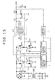
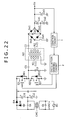
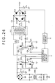
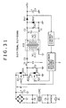
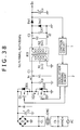
- FIG. 11 shows an example of a configuration of a power supply circuit according to a second embodiment of the present invention.
- the power supply circuit shown in FIG. 11 has a basic configuration as a multiple composite resonance type converter including a bridge full wave rectification circuit (Di, Ci) as a rectification circuit system for producing a rectification smoothed voltage Ei (DC input voltage) and adopts a half bridge coupling system for a primary side current resonance type converter similarly to the power supply circuit described hereinabove with reference to FIG. 1.
- a bridge full wave rectification circuit Di, Ci
- Ei DC input voltage
- a gap length of approximately 2.8 mm is set for a gap G formed in the inner magnetic leg of an insulating converter transformer PIT having a structure, for example, shown in FIG. 2 similarly as in the power supply circuit of the first embodiment shown in FIG. 1.
- the present power supply circuit is incorporated as a power supply, for example, in a plasma display apparatus, and therefore has a configuration for producing a secondary side DC output voltage (Eo) of 200 V or more and for being ready for a load power Po within a range from 150 W to 0 W.
- Eo secondary side DC output voltage
- the power supply circuit of the second embodiment includes a voltage doubler half wave rectification circuit as a rectification circuit connected to a secondary winding N2.
- the rectification diode Do1 is connected at the anode thereof to one end portion (winding starting end portion) of the secondary winding N2 through a series connection of a secondary side series resonance capacitor C2.
- the rectification diode Do1 is connected at the cathode thereof to the positive terminal of the smoothing capacitor Co.
- the smoothing capacitor Co is connected at the negative terminal thereof to the secondary side ground.
- the secondary winding N2 is grounded at the other end portion (winding ending end portion) thereof to the secondary side ground and connected also to the anode of the rectification diode Do2.
- the rectification diode Do2 is connected at the cathode thereof to a node between the anode of the rectification diode Do1 and the secondary side series resonance capacitor C2.
- a secondary side partial resonance capacitor Cp2 is connected in parallel to the series connection circuit of the secondary winding N2 and the secondary side series resonance capacitor C2 cooperatively forming a secondary side series resonance circuit.
- the capacitor Cp2 cooperates with a leakage inductance L2 of the secondary winding N2 to form a secondary side partial voltage resonance circuit.
- the voltage doubler half wave rectification circuit formed in such a manner as described above operates in the following manner.
- the first secondary side series resonance circuit performs rectification operation in response to the current.
- partial voltage resonance operation by the secondary side partial voltage resonance circuit including a secondary side partial resonance capacitor Cp2A is obtained at timings at which the rectification diodes Do1 and Do2 turn off.
- the voltage doubler half wave rectification circuit is formed as the rectification smoothing circuit for producing the secondary side DC output voltage Eo so that the secondary side DC output voltage Eo of a level equal to twice the alternating voltage level obtained in the secondary winding N2 is obtained.
- the number of turns of the secondary winding N2 can be reduced to 1/2 when compared with an alternative configuration producing a voltage of a level equal to that of the alternating voltage described above as in the case of, for example, a bridge full wave rectification circuit.
- the secondary winding N2 in the first modification is set to 25 T as hereinafter described.
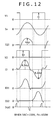
- FIGS. 12 and 13 illustrate operation waveforms of several components of the power supply circuit shown in FIG. 11.
- the resonance frequency fo2 is set so as to have a value lower than that of the resonance frequency fo1 so that the relationship of fo1 > fo2 is obtained similarly as in the first embodiment.
- the voltage V1 is a voltage across the switching element Q2 and indicates on/off timings of the switching element Q2.
- the switching current IQ2 of the switching element Q2 illustrated in FIGS. 12 and 14 flows and the switching element Q2 exhibits an on state.
- the switching current IQ2 has the zero level and the switching element Q2 exhibits an off state.
- the voltage across the switching element Q1 has a waveform shifted by 180 degrees from that of the voltage V1.
- the switching current IQ1 of the switching element Q1 has a waveform having a phase shifted by 180 degrees from that of the switching current IQ2.
- the switching element Q1 and the switching element Q2 are switched on and off alternately.
- the primary side series resonance current Io flowing through the primary side series resonance circuit has such a waveform as seen in FIGS. 12 and 13, which is a composite waveform of the switching current IQ1 and the switching current IQ2.
- the switching period of the waveforms of FIG. 13 in the case of a light load condition is shorter than that of the waveforms of FIG. 12 in the case of a heavy load.
- the stabilization control is performed such that, where the load becomes heavier and the level of the secondary side DC output voltage Eo decreases, the switching frequency decreases, but where the load becomes lighter and the level of the secondary side DC output voltage Eo increases, the switching frequency increases.
- the rectification diodes Do1 and Do2 on the secondary side are rendered conducting so that rectification current flows on the secondary side.
- the rectification current ID1 flows within a period that the alternating voltage excited in the secondary winding N2 has the positive polarity.
- the rectification current ID2 flows within another period that the alternating voltage has the negative polarity.
- the secondary side DC output voltage Eo of a level equal to twice that of the alternating voltage produced in the secondary winding N2 is produced as a voltage across the smoothing capacitor Co.
- a voltage V2 appearing between the node of the secondary side series resonance capacitor C2 and the anode of the rectification diode Do1 and the winding starting end portion of the secondary winding N2 has a waveform as follows.
- a peak level equal to the level of the secondary side DC output voltage Eo on the positive side is obtained within a period that the rectification diode Do1 conducts (within a half period that the alternating voltage excited in the secondary winding N2 has the positive polarity).
- the zero level is obtained within another period that the rectification diode Do2 conducts (within the other half period that the alternating voltage excited in the secondary winding N2 has the negative polarity) as seen in FIG. 12.
- the circuit shown in FIG. 11 operates as a voltage doubler half wave rectification circuit.
- the circuit performs charging of the smoothing capacitor Co only within the half period of the alternating voltage obtained from the secondary winding N2 to obtain the secondary side DC output voltage Eo of a level equal to twice that of the alternating voltage across the smoothing capacitor Co.
- FIGS. 12 and 13 further illustrate current ICp2 flowing to the secondary side partial resonance capacitor Cp2 provided on the secondary side.
- the current ICp2 flows at timings at which the rectification diode Do1 and the rectification diode Do2 turn off (turn on).
- the waveform of the current ICp2 indicates partial voltage resonance operation obtained at turning-off (turning-on) timings of the rectification diodes Do1 and Do2.
- the waveform of the current ICp2 indicates that reverse current generated upon turning off of the rectification diodes Do1 and Do2 flows, and suppression of the power loss (switching loss) by the rectification diodes Do1 and Do2 can be anticipated thereby as described hereinabove.
- FIG. 14 illustrates characteristics of the power supply circuit shown in FIG. 11 obtained by an experiment conducted with the power supply circuit and particularly illustrates an AC ⁇ DC power conversion efficiency and a switching frequency characteristic with respect to a load variation.
- the switching frequency fs exhibits a characteristic that the variation thereof is suppressed when compared with that of the circuit in related art, that is, a steep variation of the switching frequency fs with respect to the variation within a range from a light load condition to a no load condition is suppressed effectively.
- the necessary control range ⁇ fsA over the range of the commercial AC power supply of the AC 100 V type to the AC 200 V type is approximately 80 to 130 kHz. This sufficiently remains within the frequency variation range (approximately 50 to 200 kHz) of the switching driving IC (oscillation driving circuit 2).
- an existing switching driving IC can be used as it is for the implementation of the configuration ready for a wide range similarly to the first embodiment.
- FIG. 15 shows an example of a configuration of a power supply circuit according to a first modification to the second embodiment described above.
- the modified power supply circuit shown in FIG. 15 naturally has a basic configuration similar to that of the second embodiment and includes principal components selectively set similarly to those of the power supply circuit of FIG. 11. Consequently, in the modified power supply circuit, the coupling coefficient k of the insulating converter transformer PIT and the resonance frequencies fo1 and fo2 are set similarly to those in the power supply circuit FIG. 1.
- the power supply circuit of FIG. 15 has a configuration for being ready for a heavier load condition.
- the power supply circuit shown includes a primary side current resonance type converter including four switching elements Q1 to Q4 connected in a full bridge connection.
- FIG. 16 shows an example of a configuration of a power supply circuit according to a second modification to the second embodiment described above. Also the modified power supply circuit shown in FIG. 16 naturally has a basic configuration similar to that of the second embodiment and has a configuration for being ready for a heavier load condition.
- the modified power supply circuit includes, as a rectification current circuit system for receiving a commercial AC power supply AC (AC input voltage VAC) as an input thereto to produce a rectification smoothed voltage Ei (DC input voltage), a voltage doubler rectification circuit having a configuration similar to that of FIG. 10.
- AC AC input voltage
- VAC commercial AC power supply AC
- Ei DC input voltage
- a voltage doubler rectification circuit having a configuration similar to that of FIG. 10.
- the secondary side voltage doubler half wave rectification circuit has a configuration different from those of FIGS. 11 and 15.
- the secondary side series resonance capacitor C2 is connected in series to one end portion of the secondary winding N2, and the anode of the rectification diode Do1 is connected to the secondary side series resonance capacitor C2.
- a series connection circuit of a smoothing capacitor Co1 (first secondary side smoothing capacitor) and another smoothing capacitor Co2 (second secondary side smoothing capacitor) is connected as the secondary side smoothing capacitor for producing the secondary side DC output voltage Eo as seen in FIG. 16.
- the smoothing capacitor Co1 is connected at the positive terminal thereof to the cathode of the rectification diode Do1, and the negative terminal of the smoothing capacitor Co1 and the positive terminal of the smoothing capacitor Co2 are connected to each other.
- the negative terminal of the smoothing capacitor Co2 is connected to the secondary side ground.
- a node between the smoothing capacitor Co1 and the smoothing capacitor Co2 is connected to the other end portion of the secondary winding N2.
- the rectification diode Do2 is connected at the cathode thereof to a node between the secondary side series resonance capacitor C2 and the anode of the rectification diode Do1 and at the anode thereof to the secondary side ground.
- the secondary side partial resonance capacitor Cp2 is interposed between a node between the secondary side series resonance capacitor C2 and the cathode of the rectification diode Do2 and the secondary side ground such that it may have a parallel relationship to the series connection circuit of the secondary winding N2 and the secondary side series resonance capacitor C2. Consequently, a partial voltage (parallel) resonance circuit is formed from the secondary side partial resonance capacitor Cp2 and the leakage inductance L2 of the secondary winding N2.
- rectification current flows along a path of the rectification diode Do1 - smoothing capacitor Co1, and consequently, a voltage of a level equal to the that of the alternating voltage is produced across the smoothing capacitor Co1.
- rectification current flows along another path of the smoothing capacitor Co2 - rectification diode Do2. Consequently, a voltage of a level equal to that of the alternating voltage is produced across the smoothing capacitor Co2.
- each of the smoothing capacitors Co1 and Co2 provided on the secondary side in this instance is charged only within the half period of the alternating voltage, half wave rectification operation is obtained as the rectification operation.
- operation as a voltage doubler half wave rectification circuit is obtained also on the secondary side of the circuit shown in FIG. 16.
- the circuit shown in FIG. 16 is applied for a single range because the rectification circuit system for producing the rectification smoothed voltage Ei is formed as a voltage doubler rectification circuit.
- the circuit achieves a good responding performance of constant voltage control to a steep variation within a wide load variation range such as a switching load.
- FIGS. 15 and 16 may be further modified such that, for example, the configuration of the secondary side of FIG. 16 has a configuration of the half bridge coupling of the primary side shown in FIG. 1.
- Alto it is possible to apply the configuration of the secondary side of FIG. 16 to the full bridge configuration of the primary side shown in FIG. 15 or to conversely apply the configuration of the secondary side shown in FIG. 15 to the configuration of the voltage doubler rectification circuit of the primary side shown in FIG. 16.
- the combination of the configurations of the primary side and the secondary side may be altered suitably. This also applies to various embodiments hereinafter described.
- FIG. 17 shows an example of a configuration of a power supply circuit according to a third embodiment of the present invention.
- the power supply circuit shown in FIG. 17 has a basic configuration as a multiple composite resonance type converter.
- the converter includes a bridge full wave rectification circuit (Di, Ci) as a rectification circuit system for producing a rectification smoothed voltage Ei (DC input voltage) and adopts a half bridge coupling system for a primary side current resonance type converter similarly to the power supply circuits described hereinabove with reference to FIGS. 1 and 11.
- Di, Ci bridge full wave rectification circuit
- Ei DC input voltage
- a gap length of approximately 2.8 mm is set for a gap G formed in the inner magnetic leg of a insulating converter transformer PIT having a structure, for example, shown in FIG. 2.
- the present power supply circuit is incorporated as a power supply, for example, for a plasma display apparatus, and therefore has a configuration for producing a secondary side DC output voltage Eo of 200 V or more and for being ready for a load power Po within a range from 150 to 0 W.
- the power supply circuit shown in FIG. 17 includes a voltage doubler full wave rectification circuit as a secondary side rectification circuit.
- the secondary winding N2 in the voltage doubler full wave rectification circuit has a center tap provided thereon such that the secondary winding N2 is divided into two secondary winding sections N2A and N2B. In this instance, the center tap of the secondary winding N2 is grounded to the secondary side ground.
- An end portion of the secondary winding section N2A is a winding ending end portion of the secondary winding N2.
- the end portion of the secondary winding section N2A is connected to a node between the anode of the rectification diode Do1 and the cathode of the rectification diode Do2 through a series connection of a secondary side series resonance capacitor C2A.
- an end portion of the secondary winding section N2B is a winding starting end portion of the secondary winding N2.
- the end portion of the secondary winding section N2B is connected to a node between the anode of a rectification diode Do3 and the cathode of a rectification diode Do4 through a series connection of a secondary side series resonance capacitor C2B.
- a node between the rectification diodes Do2 and Do4 is connected to the secondary side ground.
- a node between the rectification diode Do1 and the rectification diode Do2 is connected to the positive terminal of the smoothing capacitor Co.
- the negative terminal of the smoothing capacitor Co is connected to the secondary side ground.
- two secondary side partial resonance capacitors Cp2A and Cp2B are provided.
- the secondary side partial resonance capacitor Cp2A is inserted between a node between the anode of the rectification diode Do1 and the cathode of the rectification diode Do2 and the secondary side ground.
- the secondary side partial resonance capacitor Cp2B is inserted between a node between the anode of the rectification diode Do3 and the cathode of the rectification diode Do4 and the secondary side ground.
- the voltage doubler full wave rectification circuit formed in such a connection scheme as described above performs such rectification operation as described below.
- the voltage doubler full wave rectification circuit can be divided into first and second voltage doubler half wave rectification circuits.
- the first voltage doubler half wave rectification circuit is formed from the [secondary winding section N2A, secondary side series resonance capacitor C2A, rectification diodes Do1 and Do2, and secondary side partial resonance capacitor Cp2A].
- the second voltage doubler half wave rectification circuit is formed from the [secondary winding section N2B, secondary side series resonance capacitor C2B, rectification diodes Do3 and Do4, and secondary side partial resonance capacitor Cp2B].
- a first secondary side series resonance circuit is formed from the leakage inductance component (L2A) of the secondary winding section N2A and the capacitance of the secondary side series resonance capacitor C2A.
- a second secondary side series resonance circuit is formed from the leakage inductance component (L2B) of the secondary winding section N2B and the capacitance of the secondary side series resonance capacitor C2B.
- the secondary side partial resonance capacitor Cp2A inserted in such a manner as described hereinabove is connected in parallel to the series connection of the secondary winding section N2A - secondary side series resonance capacitor C2A. Accordingly, a secondary side partial voltage resonance circuit corresponding to the first voltage doubler half wave rectification circuit is formed from the capacitance of the secondary side partial resonance capacitor Cp2A itself and the leakage inductance L2A of the secondary winding section N2A.
- the secondary side partial resonance capacitor Cp2B is connected in parallel to the series connection of the secondary winding section N2B - secondary side series resonance capacitor C2B. Accordingly, another secondary side partial voltage resonance circuit corresponding to the second voltage doubler half wave rectification circuit is formed from the capacitance of the secondary side partial resonance capacitor Cp2B itself and the leakage inductance L2B of the secondary winding section N2B.
- the first voltage doubler half wave rectification circuit performs rectification operation in the following manner.
- rectification current flows along a path of the secondary winding section N2A - rectification diode Do2 - secondary side series resonance capacitor C2A thereby to charge the rectification current into the secondary side series resonance capacitor C2A.
- a voltage of a level equal to that of the alternating voltage induced in the secondary winding section N2A is produced across the secondary side series resonance capacitor C2A.
- the first voltage doubler half wave rectification circuit performs voltage doubler rectification operation.
- the voltage doubler rectification operation produces a voltage across the secondary side series resonance capacitor C2A that has a level equal to that of the alternating voltage of the secondary winding section N2A within the half period of the alternating voltage of the secondary winding section N2A and charges the smoothing capacitor Co with a voltage of a superposed level of the alternating voltage of the secondary winding section N2A and the voltage across the secondary side series resonance capacitor C2A within the other half period of the alternating voltage of the secondary winding section N2A.
- the first voltage doubler half wave rectification circuit obtains a voltage of a level equal to twice that of the alternating voltage of the secondary winding section N2A as the voltage across the smoothing capacitor Co.
- the first secondary side series resonance circuit performs rectification operation in response to the current.
- partial voltage resonance operation by the secondary side partial voltage resonance circuit including the secondary side partial resonance capacitor Cp2A is obtained at timings at which the rectification diodes Do1 and Do2 turn off.
- the second voltage doubler half wave rectification circuit voltage doubler half wave rectification operation similar to that of the first voltage doubler half wave rectification circuit is executed at periodical timings shifted by the half period from those by the rectification operation of the first voltage doubler half wave rectification circuit described hereinabove by the [secondary winding section N2B, secondary side series resonance capacitor C2B and rectification diodes Do3 and Do4]. Further, as a result of the rectification operation, the second secondary side series resonance circuit performs rectification operation. Furthermore, at timings at which the rectification diodes Do3 and Do4 turn off in such rectification operation, the secondary side partial voltage resonance circuit including the secondary side partial resonance capacitor Cp2B performs partial voltage resonance operation.
- the entire rectification circuit connected to the secondary winding N2 performs voltage doubler full wave rectification operation.
- the voltage doubler full wave rectification operation charges the smoothing capacitor Co with a charging potential equal to twice the alternating voltage induced in the secondary winding sections N2A and N2B within every period of half wave wherein the alternating voltage of the secondary winding N2 is in the positive/negative.
- the smoothing capacitor Co obtains the secondary side DC output voltage Eo.
- the secondary side DC output voltage Eo is a rectification smoothed voltage equal to twice the alternating voltage induced in the secondary winding sections N2A and N2B.
- FIGS. 18 and 19 illustrate operation waveforms of several components of the power supply circuit shown in FIG. 17.
- FIGS. 18 and 19 illustrate the voltage V1 across the switching element Q2 and further illustrate on/off timings of the switching element Q2. Also in this instance, the voltage across the switching element Q1 has a waveform shifted by 180 degrees from that of the voltage V1. Similarly, also the switching current IQ1 of the switching element Q1 has a waveform having a phase shifted by 180 degrees from that of the switching current IQ2. In other words, the switching element Q1 and the switching element Q2 are switched on and off alternately.
- the primary side series resonance current Io flowing through the primary side series resonance circuit has such a waveform as seen in FIGS. 18 and 19, which is a composite waveform of the switching current IQ1 and the switching current IQ2.
- the stabilization control according to the switching frequency control method is performed such that the switching frequency increases as the level of the secondary side DC output voltage Eo increases similarly as in the first and second embodiments.
- the secondary winding currents I2A and I2B exhibit a peak level (positive and negative absolute values) of 2 Ap at the maximum load power as seen in FIG. 18.
- the potential V2 appearing between the node of the secondary side series resonance capacitor C2A and the anode of the rectification diode Do1 and the winding staring end of the secondary winding section N2A has a waveform as follows.
- a peak level equal to that of the secondary side DC output voltage Eo is obtained on the positive side within the half period of the alternating voltage excited in the secondary winding N2.
- the zero level is obtained within the other half period of the alternating voltage excited in the secondary winding N2.
- the voltage V3 appearing between the node of the secondary side series resonance capacitor C2B and the anode of the rectification diode Do3 and the winding staring end portion of the secondary winding section N2B has a waveform as follows.
- a peak level equal to that of the secondary side DC output voltage Eo is obtained on the positive side within the other half period of the alternating voltage excited in the secondary winding N2.
- the zero level is obtained within the one half period of the alternating voltage excited in the secondary winding N2.
- the circuit shown in FIG. 17 operates as a voltage doubler full wave rectification circuit.
- the circuit charges the smoothing capacitor Co within each half period of the alternating voltage induced in the secondary winding N2 thereby to obtain the secondary side DC output voltage Eo of a level equal to twice the level of the alternating voltage obtained in the secondary winding N2 across the smoothing capacitor Co.
- FIGS. 18 and 19 further illustrate the current ICp2 flowing to the secondary side partial resonance capacitor Cp2A provided on the secondary side. Also in this instance, the current ICp2 flows at timings at which the rectification diode Do1 and the rectification diode Do2 turn off, and it is illustrated that reverse current generated upon turning off of the rectification diodes Do1 and Do2 flows.
- the current (not shown) flowing to the secondary side partial resonance capacitor Cp2B provided in the second voltage doubler half wave rectification circuit has a waveform shifted by 180° from that of the current ICp2. Consequently, also for the rectification diode Do3 and the rectification diode Do4, a path for allowing reverse current to flow upon turning off is formed, and as a result, reduction of the switching loss by the rectification diodes Do provided on the secondary side can be anticipated.
- FIG. 20 illustrates characteristics of the power supply circuit shown in FIG. 17 and particularly illustrates an AC ⁇ DC power conversion efficiency and a switching frequency control characteristic with respect to a load variation.
- the power supply circuit of the third embodiment achieves a power conversion efficiency having a value a little higher than that of the power supply circuit of the second embodiment described hereinabove, this arises from the fact that the secondary side voltage doubler rectification operation is changed over from the half wave rectification operation to the full wave rectification operation.
- the secondary winding N2 in the present embodiment including the voltage doubler rectification circuit can be formed with a reduced number of turns.
- the switching frequency fs in this instance exhibits a characteristic that the variation thereof is suppressed when compared with that of the circuit in related art, that is, a steep variation of the switching frequency fs with respect to the variation within a range from a light load condition to a no load condition is suppressed effectively.
- the necessary control range ⁇ fsA over the range of the commercial AC power supply of the AC 100 V type to the AC 200 V type is approximately 80 to 140 kHz. This sufficiently remains within the frequency variation range (approximately 50 to 200 kHz) of the switching driving IC (oscillation driving circuit 2).
- an existing switching driving IC can be used as it is for the implementation of the configuration ready for a wide range similarly to the first and second embodiments.
- FIG. 21 shows an example of a configuration of a power supply circuit according to a first modification of the third embodiment described above.
- the modified power supply circuit shown in FIG. 21 naturally has a basic configuration similar to that of the third embodiment and includes principal components selectively set similarly to those of the power supply circuit of FIG. 17. Consequently, in the modified power supply circuit, the coupling coefficient k of the insulating converter transformer PIT and the resonance frequencies fo1 and fo2 are set similarly to those in the power supply circuit of FIG. 1.
- the power supply circuit of FIG. 21 has a configuration for being ready for a heavier load condition.
- the power supply circuit shown includes a primary side current resonance type converter including four switching elements Q1 to Q4 connected in a full bridge connection.
- FIG. 22 shows an example of a configuration of a power supply circuit according to a second modification of the third embodiment described above. Also the modified power supply circuit shown in FIG. 22 naturally has a basic configuration similar to that of the third embodiment and has a configuration for being ready for a heavier load condition.
- the modified power supply circuit includes, as the rectification current circuit system for receiving a commercial AC power supply AC (AC input voltage VAC) as an input thereto to produce the rectification smoothed voltage Ei (DC input voltage), a voltage doubler rectification circuit having a configuration similar to that of FIG. 10.
- AC AC input voltage
- VAC commercial AC power supply AC
- Ei DC input voltage
- the secondary side voltage doubler full wave rectification circuit has a different circuit configuration from that of FIG. 17.
- the secondary winding N2 is not divided by provision of a center tap, and a bridge rectification circuit formed from rectification diodes Do1 to Do4 connected in a bridge connection is provided as the rectification circuit on the secondary side.
- the smoothing capacitor Co for producing the secondary side DC output voltage Eo is formed from a series connection circuit of a smoothing capacitor Co1 (second secondary side smoothing capacitor) and another smoothing capacitor Co2 (third secondary side smoothing capacitor) and a smoothing capacitor Co3 (first secondary side smoothing capacitor) connected in parallel to the series connection circuit.
- the negative terminal of the smoothing capacitor Co2 and the negative terminal of the smoothing capacitor Co3 are connected to the secondary side ground.
- a node between the rectification diode Do1 and the rectification diode Do2 is referred to as first terminal; a node between the rectification diode Do1 and the rectification diode Do3 is referred to as second terminal; a node between the rectification diode Do3 and the rectification diode Do4 is referred to as third terminal; and a node between the rectification diode Do4 and the rectification diode Do2 is referred to as fourth terminal.
- the first terminal is connected to one end portion of the secondary winding N2 through a series connection of the secondary side series resonance capacitor C2.
- the second terminal is connected to a node between the positive terminal of the smoothing capacitor Co1 and the positive terminal of the smoothing capacitor Co3.
- the third terminal is connected to the other end portion of the secondary winding N2, and is connected, at the node thereof, to a node between the smoothing capacitor Co1 and the smoothing capacitor Co2.
- the fourth terminal is connected to the secondary side ground.
- rectification current flows along a path of the [secondary side series resonance capacitor C2 rectification diode Do1 smoothing capacitor Co3 rectification diode Do4]. Further, within the period, the rectification current is branched and flows also through the rectification diode Do1 smoothing capacitor Co1.
- rectification current flows along another path of the [rectification diode Do3 smoothing capacitor Co3 rectification diode Do2 secondary side series resonance capacitor C2]. Also within this period, the rectification current is branched and flows also through the smoothing capacitor Co2 rectification diode Do3.
- the rectification current is branched and flows in such a manner as described above, operation of charging the rectification current into the smoothing capacitor Co1 within one of two half periods of the alternating voltage is performed, and within this period, a voltage of a level equal to that of the alternating voltage is produced across the smoothing capacitor Co1.
- the secondary side of the circuit shown in FIG. 22 operates as a voltage doubler full wave rectification circuit which performs operation of charging rectification current into the secondary side smoothing capacitor within each one half period of the alternating voltage excited in the secondary winding N2 to produce the secondary side DC output voltage Eo of a level equal to twice that of the alternating voltage across the secondary side smoothing capacitor.
- the number of turns of the secondary winding N2 can be set to 25 T equal to that of FIG. 17.
- both of the merit that miniaturization of a transformer and simplification of a winding step similar to those where a configuration of a voltage doubler half wave rectification circuit is adopted and the merit of reduction of the power loss arising from employment of full-wave rectification can be achieved.
- the secondary side partial resonance capacitor Cp2 is inserted between the first terminal (node of D1 and D2: positive input terminal) and the third terminal (node of D3 and D4: negative input terminal) of the bridge rectification circuit described hereinabove such that the secondary side partial resonance capacitor Cp2 is connected in parallel to the series connection circuit of the secondary winding N2 and the secondary side series resonance capacitor C2. Consequently, the capacitance of the secondary side partial resonance capacitor Cp2 and the leakage inductance L2 of the secondary winding N2 cooperate with each other to form a partial voltage resonance circuit which performs voltage resonance operation only at timings at which the rectification diodes Do1, Do2, Do3 and Do4 turn off.
- circuit shown in FIG. 22 is used for an application ready for a single range, also in this instance, the merit that a high speed response of constant voltage control can be anticipated is achieved.
- FIGS. 21 and 22 can be further modified such that the primary side has the configuration shown in FIG. 17 or the configurations of the primary side are exchanged between each other.
- FIG. 23 shows an example of a configuration of a switching power supply circuit according to a fourth embodiment of the present invention.
- the circuit configuration itself of the power supply circuit shown in FIG. 23 is a multiple (composite) resonance type converter similar to that shown in FIG. 1.
- the primary side includes a combination of a partial voltage resonance circuit with a separately excited current resonance type converter according to the half bridge coupling system.
- the secondary side includes a secondary side series resonance capacitor C2 connected in series to a secondary winding N2 to form a secondary side series resonance circuit and includes a bridge full wave rectification circuit as a secondary side rectification circuit.
- the secondary side includes a secondary side partial resonance capacitor Cp2 which forms a secondary side partial voltage resonance circuit.
- the resonance frequency fo1 of the primary side series resonance circuit and the resonance frequency fo2 of the secondary side series resonance circuit are set so as to satisfy a relationship represented by fo1 ⁇ fo2
- the resonance frequency fo2 of the secondary side series resonance circuit is set so as to be within approximately 1.5 times that of the resonance frequency fo1.
- the resonance frequency fo2 of the secondary side series resonance circuit is set within a range from approximately 1.4 times to approximately 1.3 times the resonance frequency fo1 of the primary side series resonance circuit. More particularly, the resonance frequency fo1 is set to a predetermined value of fo1 ⁇ 70 kHz, and the resonance frequency fo2 is set to another predetermined value of fo2 ⁇ 90 kHz.
- k 0.65 was obtained as the coupling coefficient k of the insulating converter transformer PIT itself.
- the resonance capacitors for forming the primary side series resonance circuit, secondary side series resonance circuit, primary side partial voltage resonance circuit and secondary side partial voltage resonance circuit were selectively set in the following manner:
- the secondary side DC output voltage Eo was set to a rated level of 135 V.
- the resonance frequency fo1 of the primary side series resonance circuit of fo1 ⁇ 70 kHz is set from the leakage inductance L1 of the primary winding N1 obtained from the structure of the insulating converter transformer PIT described above and the capacitance of the primary side series resonance capacitor C1.
- the resonance frequency fo2 of the secondary side series resonance circuit of fo2 ⁇ 90 kHz is set from the leakage inductance L2 of the secondary winding N2 obtained from the structure of the insulating converter transformer PIT described above and the capacitance of the secondary side series resonance capacitor C2.
- the voltage V1 of a rectangular waveform is a voltage across the switching element Q2 and indicates on/off timings of the switching element Q2.
- the voltage V1 has a waveform wherein it exhibits the 0 level within an on period that the switching element Q2 is conducting and is in an on state, but is clamped at the level of the rectification smoothed voltage Ei within an off period that the switching element Q2 is not conducting.
- switching current IQ2 having a waveform illustrated in FIG. 24 flows in a switching circuit system formed from the switching element Q2 and a clamp diode DD2. Further, the switching current IQ2 exhibits the 0 level within an off period of the switching element Q2.
- the voltage across the other switching element Q1 and the switching current flowing to the switching circuit (Q1, DD1) have waveforms having phases displaced by 180° from those of the voltage V1 and the switching current IQ2, respectively.
- the switching element Q1 and the switching element Q2 perform switching operations at the same periodic timings such that they are turned on/off alternately.
- the primary side series resonance current Io flowing to the primary side series resonance circuit (L1-C1) has such a waveform as seen in FIG. 24 because it is formed by combination of the switching currents flowing through the switching circuits (Q1, DD1) and (Q2, DD2).
- the voltage V1 indicates a variation that, when the load becomes heavier and the level of the secondary side DC output voltage Eo drops, the switching frequency becomes lower, but when the load becomes lighter and the level of the secondary side DC output voltage Eo rises, the switching frequency becomes higher.
- an alternating voltage V2 of a waveform illustrated in FIG. 24 is induced in the secondary winding N2 of the insulating converter transformer PIT.
- the length of one period of the alternating voltage V2 corresponds to the switching period of the primary side.
- the rectification diodes [Do1, Do4] of the secondary side conduct and rectification current flows, but within the other half period of the alternating voltage V2, the rectification diodes [Do2, Do3] of the secondary side conduct and rectification current flows.
- the secondary winding current I2 flowing through the secondary winding N2 is obtained by combination of the rectification currents flowing for every one half period of the alternating voltage V2, and a waveform shown in FIG. 24 is obtained.
- the switching frequency control method upper side control
- the necessary control range of the switching frequency fs is 123.5 to 114.9 kHz, and the variation control range (necessary control range) ⁇ fs2 illustrated in FIG.
- the upper limit to the switching driving frequency of the switching element driving IC (oscillation driving circuit 2) at present is approximately 200 kHz. Accordingly, the range of the switching frequency fs from approximately 123.5 to 73.5 kHz given hereinabove is obtained sufficiently by the switching driving IC at present.
- the power supply circuit of the present embodiment can be ready for a wide range only by switching frequency control while the configuration of the switching driving circuit system at present is maintained because the necessary control range of the switching frequency fs is reduced significantly to a comparatively low frequency region.
- the relationship of the resonance frequency fo2 of the secondary side series resonance circuit and the resonance frequency fo1 of the primary side series resonance circuit is set such that the resonance frequency fo2 of the secondary side series resonance circuit is higher.
- the secondary side series resonance capacitor C2 is set to a capacitance lower than a fixed level.
- the capacitance of the secondary side series resonance capacitor C2 is set to a comparatively low value. Consequently, for example, a small part can be used actually as the secondary side series resonance capacitor C2, and this is advantageous in reduction in size and weight of the circuit.
- the primary side series resonance current Io flowing to the primary side series resonance circuit sometimes exhibits a substantially M-shaped waveform in the proximity of a peak after every one half period.
- the resonance frequency fo2 of the secondary side series resonance circuit drops until the frequency difference between the resonance frequency fo1 of the primary side series resonance circuit and the resonance frequency fo2 of the secondary side series resonance circuit becomes within a fixed range.
- the level of the M-shaped peak portion of the primary side series resonance current Io described hereinabove has a tendency that it increases as the capacitance of the secondary side series resonance capacitor C2 decreases (as the resonance frequency fo2 of the secondary side series resonance circuit is raised). Then, since the increase of the level of the M-shaped peak portion of the primary side series resonance current Io makes a cause of, for example, increase of the switching loss at the switching elements Q1 and Q2, it gives rises to a drop of the power conversion efficiency. Further, since the M-shaped peak portion of the primary side series resonance current Io appears, for example, as a variation component of the secondary side DC output voltage Eo, the increase makes a factor of expansion of the necessary control range ( ⁇ fs) in the switching frequency control. Accordingly, the capacitance of the secondary side series resonance circuit (resonance frequency of the secondary side series resonance circuit) should be set taking it into consideration that the reduction of the power conversion efficiency and the expansion of the necessary control range remain within a sufficiently permissible range for practical utilization.
- the resonance frequency fo2 of the secondary side series resonance circuit should remain within a range of approximately 1.5 times the resonance frequency fo1 of the primary side series resonance circuit.
- FIG. 26 shows an example of a configuration of a power supply circuit according to a first modification to the fourth embodiment described above.
- the modified power supply circuit shown in FIG. 26 naturally has a basic configuration similar to that of the fourth embodiment and includes principal components selectively set similarly to those of the power supply circuit of FIG. 23.
- the power supply circuit of FIG. 26 has a configuration for being ready for a heavier load condition.
- the power supply circuit shown includes a primary side current resonance type converter including four switching elements Q1 to Q4 connected in a full bridge connection.
- the four switching elements Q1 to Q4 are driven by the oscillation driving circuit 2.
- the oscillation driving circuit 2 performs switching driving of the set of the switching elements [Q1, Q4] and the set of the switching elements [Q2, Q3] so as to turn on/off alternately.
- the power supply circuit of the present modification includes a high frequency inductor L11.
- the high frequency inductor L11 in this instance is inserted in series between the primary winding N1 of the insulating converter transformer PIT and the switching output point of the switching elements Q1 and Q2 as described hereinabove. In short, the high frequency inductor L11 is connected in series to the primary winding N1.
- the inductance component which forms the primary side series resonance circuit is a combination of the inductance of the high frequency inductor L11 and the leakage inductance L1 of the leakage inductance L1, that is, L1 + L11.
- the inductance of the high frequency inductor L11 can be equivalently regarded as a leakage inductance component of the primary winding N1. Accordingly, the leakage inductance of the primary side of the insulating converter transformer PIT is given by L11 + L1.
- the coupling coefficient of the insulating converter transformer PIT itself is represented by k
- a value lower than the coupling coefficient k is obtained as a composite coupling coefficient kt of the insulating converter transformer PIT in the power supply circuit.
- the coupling degree of the insulating converter transformer PIT in the power supply circuit is set lower than the coupling coefficient k by the structure itself of the insulating converter transformer PIT.
- the power supply circuit does not include an inductor connected in series to the primary winding N1. Therefore, a loose coupling state of such a degree that a unimodal characteristic is obtained as indicated as the characteristic curve 3 of FIG. 6 is obtained as the coupling degree between the primary side and the secondary side by the coupling coefficient k of the insulating converter transformer PIT itself. More particularly, the coupling coefficient k of the insulating converter transformer PIT itself is set to a value within approximately 0.65.
- the composite coupling coefficient kt should be set to a value, for example, within 0.65 when a power supply circuit ready for a wide range with a unimodal characteristic described hereinabove is to be constructed.
- the composite coupling coefficient kt conforms to the total primary side leakage inductance (L11 + L1) obtained by combination of the inductance of the high frequency inductor L11 and the leakage inductance L1 of the primary winding N1. Accordingly, in order to set the composite coupling coefficient kt to a value within approximately 0.65, the composite coupling coefficient kt of the insulating converter transformer PIT itself is set to a value higher than 0.65.
- the composite coupling coefficient kt of the insulating converter transformer PIT itself is set to approximately 0.75.
- the shortage of the leakage inductance for setting the composite coupling coefficient kt to approximately 0.65 is obtained from the inductance of the high frequency inductor L11.
- the gap G of the inner magnetic leg is set to a gap length of approximately 2.8 mm as described hereinabove with reference to FIG. 2.
- the gap length of the gap G in a structure similar to that of FIG. 2 is set as short as, for example, approximately 1.6 mm.
- eddy current is generated in the proximity of the gap G.
- eddy current gives rise to the power loss and gives rise to a drop of the power conversion efficiency as much.
- the dropping tendency of the AC DC power conversion efficiency arising from the eddy current loss becomes conspicuous as the level of the AC input voltage rises. Accordingly, the power supply circuit ready for a wide range suffers from a problem that the ACD C power conversion efficiency drops when it is used with a voltage of the AC 200 V type rather than when it is used with another voltage of the AC 100 V type.
- the high frequency inductor L11 is connected to the primary winding N1 so as to equivalently increase the leakage inductance of the primary winding N1 by the inductance of the high frequency inductor L11 thereby to set the composite coupling coefficient kt of the insulating converter transformer PIT in the power supply circuit to 0.65 or less.
- the gap length of the gap G can be set to approximately 1.6 mm as described hereinabove. In other words, the gap length can be suppressed to a level with which the problem of increase of eddy current does not occur.
- the inductance of the high frequency inductor L11 is actually set to a predetermined value within a range such as, for example, approximately 30 H. Further, since the inductance of the high frequency inductor L11 may be approximately several tens H in this manner, the high frequency inductor L11 can be formed in a small size and also the power loss by a resistance component of the high speed inductor L11 is so low that it can be almost ignored.
- FIG. 27 shows an example of a configuration of a power supply circuit according to a second modification to the fourth embodiment described above. Also the modified power supply circuit shown in FIG. 27 naturally has a basic configuration similar to that of the fourth embodiment and has a configuration for being ready for a heavier load condition.
- the modified power supply circuit includes, as a rectification current circuit system for receiving a commercial AC power supply AC (AC input voltage VAC) as an input thereto to produce a rectification smoothed voltage Ei (DC input voltage), a voltage doubler rectification circuit for producing a rectification smoothed voltage Ei of a level equal to twice that of the AC input voltage VAC.
- AC input voltage VAC AC input voltage
- VAC DC input voltage
- a voltage doubler rectification circuit for producing a rectification smoothed voltage Ei of a level equal to twice that of the AC input voltage VAC.
- a rectification smoothing circuit system for producing the DC input voltage (rectification smoothed voltage Ei) is formed as a voltage doubler rectification circuit in this manner is a configuration ready for a single range only of the AC 100 V type, the merit of enhancement of the responding performance of constant voltage control is obtained also by use in the single range similarly as in the power supply circuits described hereinabove with reference to FIGS. 10, 16 and 22.
- the high frequency inductor L11 connected in series to the primary winding N1 in the first modification shown in FIG. 26 is omitted, and instead, a high frequency inductor L12 is connected in series to the secondary winding N2.
- the high frequency inductor L12 is inserted between one of end portions of the secondary winding N2 and a node between the anode of the rectification diode Do3 and the cathode of the rectification diode Do4.
- the primary side series resonance circuit is formed from the leakage inductance L1 of the primary winding N1 and the capacitance of the primary side series resonance capacitor C1.
- the secondary side series resonance circuit is formed from the leakage inductance L2 of the secondary winding N2, the inductance of the high frequency inductor L12 and the capacitance of the secondary side series resonance capacitor C2.
- the apparent inductance of the secondary winding side of the insulating converter transformer PIT increases by the inductance of the high frequency inductor L12. Also where the leakage inductance of the secondary side of the insulating converter transformer PIT increases in this manner, the composite coupling coefficient kt of the insulating converter transformer PIT decreases from the coupling coefficient k of the insulating converter transformer PIT itself.
- the insulating converter transformer PIT itself can be set such that it has a basic structure, for example, shown in FIG. 2 and the gap length of the gap G of the inner magnetic leg is set to approximately 1.6 mm.
- the high frequency inductor L12 connected in series to the secondary winding N2 in the second modification to the fourth embodiment may be combined with the current resonance type converter of the full bridge coupling system in the second modification to the fourth embodiment.
- the high frequency inductor L11 connected in series to the primary winding N1 in the first modification to the fourth embodiment may be combined with the configuration of the primary side in the second modification to the fourth embodiment which includes a voltage doubler rectification circuit and a current resonance type converter of the half bridge coupling system.
- FIG. 28 shows an example of a configuration of a power supply circuit according to a fifth embodiment of the present invention.
- the power supply circuit of the fifth embodiment has a circuit configuration similar to that of FIG. 17.
- the power supply circuit includes a full wave rectification circuit (Di, Ci) as a rectification circuit system for producing a rectification smoothed voltage Ei (DC input voltage), and a primary side current resonance type converter which has a basic configuration as a multiple complicated resonance type converter which adopts the half bridge coupling system.
- the power supply circuit includes a secondary side series resonance circuit formed from the secondary winding N2 and a secondary side resonance capacitor.
- the power supply circuit includes a voltage doubler full wave rectification circuit as a rectification circuit connected to the secondary winding N2.
- the power supply circuit of the fifth embodiment shown in FIG. 28 includes the voltage doubler full wave rectification circuit in this manner, where it is configured in the same specifications as those in the power supply circuit of the fourth embodiment shown in FIG. 23 in regard to the AC input voltage condition, load condition and level of the secondary side DC output voltage Eo, the number of turns of each of the secondary winding sections N2A and N2B can be set to 12 T which is 1/2 the number of turns of the secondary winding N2 of, for example, the power supply circuit of FIG. 23.
- the other components of the power supply circuit may be selectively set same as those of the power supply circuit of the fourth embodiment with which the experiment results of FIGS. 24 and 25 were obtained.
- the resonance frequency fo1 of the primary side series resonance circuit is set to a predetermined value of fo1 ⁇ 70 kHz and the resonance frequency fo2 of the secondary side series resonance circuit is set to another predetermined value of fo2 ⁇ 90 kHz similarly as in the power supply circuit of the fourth embodiment.
- the necessary control range for the switching frequency fs for the individual ranges for power supplies of the AC 100 V type and the AC 200 V type is smaller than 9 kHz.
- the necessary control range remains sufficiently low with respect to 200 kHz which is an upper limit to the switching driving frequency of a switching element driving IC (oscillation driving circuit 2) at present.
- FIG. 29 shows an example of a configuration of a power supply circuit according to a first modification to the fifth embodiment described above.
- the modified power supply circuit adopts, as a configuration of the primary side and the insulating converter transformer PIT, a configuration ready for a heavy load similar to that of the power supply circuit of the first modification to the fourth embodiment described hereinabove with reference to FIG. 26.
- the primary side current resonance type converter has a configuration of the full bridge coupling system.
- circuit of FIG. 29 includes a voltage doubler full wave rectification circuit of a circuit configuration different from that of FIG. 28 as the secondary side rectification circuit.
- only one secondary side partial resonance capacitor Cp2 is provided as the secondary side partial resonance capacitor.
- the secondary side partial resonance capacitor Cp2 is inserted between a node between the anode of the rectification diode Do1 and the rectification diode Do2 and another node of the anode of the rectification diode Do3 and the cathode of the rectification diode Do4.
- the secondary side partial resonance capacitor Cp2 is used as a capacitance for forming a secondary side partial voltage resonance circuit (parallel resonance circuit) commonly by the first voltage doubler half wave rectification circuit and the second voltage doubler half wave rectification circuit
- the set of the rectification diodes Do1 and Do4 and the set of the rectification diodes Do2 and Do3 turn on/off at alternate timings.
- the partial voltage resonance circuits are formed in such a manner as described above, partial voltage resonance operation is obtained appropriately at timings at which the rectification diodes Do1 and Do4 are turned off and timings at which the rectification diodes Do2 and Do3 are turned off.
- FIG. 30 shows an example of a configuration of a power supply circuit according to a second modification to the fifth embodiment described above.
- the modified power supply circuit adopts, as a configuration of the primary side and the insulating converter transformer PIT, a configuration ready for a heavy load similar to that of the power supply circuit of the second modification to the fourth embodiment described hereinabove with reference to FIG. 27.
- the modified power supply circuit includes a voltage doubler rectification circuit as a rectification circuit system for producing the rectification smoothed voltage Ei (DC input voltage), and the primary side current resonance type converter uses a half bridge coupling system in combination.
- the power supply circuit adopts a configuration similar to that of the second modification to the fourth embodiment described hereinabove with reference to FIG. 27.
- the power supply circuit includes a high frequency inductor on the secondary side.
- the secondary side rectification circuit is formed as a voltage doubler full wave rectification circuit similar to that in the first modification to the fifth embodiment of FIG. 29, as the high frequency inductor on the secondary side, actually two high frequency inductors L12A and L12B are provided individually corresponding to the first voltage doubler half wave rectification circuit and the second voltage doubler half wave rectification circuit.
- the high frequency inductor L12A is inserted in series between the secondary winding section N2A and the secondary side series resonance capacitor C2A such that it has a series connection relationship to the secondary winding section N2A in the first voltage doubler half wave rectification circuit.
- the high frequency inductor L12B is inserted in series between the secondary winding section N2B and the secondary side series resonance capacitor C2B such that it has a series connection relationship to the secondary winding section N2B in the second voltage doubler half wave rectification circuit.
- the high frequency inductor L12A has a relationship that it is connected in series to the secondary winding section N2A in the first voltage doubler half wave rectification circuit.
- the high frequency inductor L12B is inserted in series between the secondary winding section N2B and the secondary side series resonance capacitor C2B, it has a relationship that it is connected in series to the secondary winding section N2B in the second voltage doubler half wave rectification circuit.
- the secondary side partial resonance capacitor Cp2 cooperates, first in the first voltage doubler half wave rectification circuit, with the secondary side leakage inductance component of the insulating converter transformer PIT obtained by combination of the leakage inductance L2A of the secondary winding section N2A and the inductance of a high frequency inductor L12A to form a partial voltage resonance circuit.
- the secondary side partial resonance capacitor Cp2 cooperates, in the second voltage doubler half wave rectification circuit, with the secondary side leakage inductance component of the insulating converter transformer PIT obtained by combination of the leakage inductance L2B of the secondary winding section N2B and the inductance of another high frequency inductor L12B to form another partial voltage resonance circuit.
- FIG. 31 shows an example of a configuration of a power supply circuit according to a sixth embodiment of the present invention.
- the power supply circuit of the sixth embodiment has a circuit configuration similar to that of FIG. 11.
- the power supply circuit includes a full wave rectification circuit (Di, Ci) as a rectification circuit system for producing a rectification smoothed voltage Ei (DC input voltage), and a primary side current resonance type converter which has a basic configuration as a multiple complicated resonance type converter which adopts the half bridge coupling system.
- the power supply circuit includes a secondary side series resonance circuit formed from the secondary winding N2 and a secondary side resonance capacitor.
- the power supply circuit includes a voltage doubler half wave rectification circuit as a rectification circuit connected to the secondary winding N2.
- the power supply circuit of the sixth embodiment shown in FIG. 31 includes the voltage doubler half wave rectification circuit in this manner, where it is configured in the same specifications as those in the power supply circuit of the fourth embodiment shown in FIG. 23 in regard to the AC input voltage condition, load condition and level of the secondary side DC output voltage Eo, the number of turns of the secondary winding N2 can be set to 12 T which is 1/2 the number of turns in the first embodiment and hence can be reduced, for example, from that where the secondary side rectification circuit is an ordinary full wave rectification circuit or voltage doubler full wave rectification circuit.
- the other components of the power supply circuit may be selectively set same as those of the power supply circuit of the fourth embodiment with which the experiment results of FIGS. 24 and 25 were obtained.
- the resonance frequency fo1 of the primary side series resonance circuit is set to a predetermined value of fo1 ⁇ 70 kHz and the resonance frequency fo2 of the secondary side series resonance circuit is set to another predetermined value of fo2 ⁇ 90 kHz similarly as in the power supply circuits of the fourth and fifth embodiments.
- the necessary control range for the switching frequency fs for the individual ranges for power supplies of the AC 100 V type and the AC 200 V type is smaller than 10 kHz.
- the necessary control range remains sufficiently low with respect to 200 kHz which is an upper limit to the switching driving frequency of a switching element driving IC (oscillation driving circuit 2) at present.
- FIG. 32 shows an example of a configuration of a power supply circuit according to a first modification to the sixth embodiment described above.
- the modified power supply circuit adopts, as a configuration of the primary side and the insulating converter transformer PIT, a configuration ready for a heavy load similar to that of the power supply circuit of the first modification to the second and fourth embodiments described hereinabove with reference to FIGS. 26 and 29 and so forth.
- the primary side current resonance type converter has a configuration of the full bridge coupling system.
- the secondary side of the insulating converter transformer PIT includes a voltage doubler half wave rectification circuit similar to that in the sixth embodiment shown in FIG. 31.
- FIG. 33 shows an example of a configuration of a power supply circuit according to a second modification to the sixth embodiment described above.
- the modified power supply circuit adopts, as a configuration of the primary side and the insulating converter transformer PIT, a configuration ready for a heavy load similar to that of the power supply circuit of the second modification to the fourth embodiment described hereinabove with reference to FIG. 27.
- the modified power supply circuit includes a voltage doubler rectification circuit as a rectification circuit system for producing the rectification smoothed voltage Ei (DC input voltage), and uses a primary side current resonance type converter of a half bridge coupling system in combination.
- the secondary side includes the high frequency inductor.
- the secondary side rectification circuit is formed as a voltage doubler half wave rectification circuit similar to that shown in FIG. 31.
- the high frequency inductor L12 can be inserted in series between one end of the secondary winding N2 and the secondary side series resonance capacitor C2 in such a manner as seen in FIG. 33.
- FIG. 34 shows an example of a configuration of a switching power supply circuit according to a seventh embodiment of the present invention.
- the circuit configuration itself of the power supply circuit shown in FIG. 34 is a multiple (composite) resonance type converter similar to that shown in FIGS. 1, 23 and so forth.
- the primary side includes a combination of a partial voltage resonance circuit with a separately excited current resonance type converter according to the half bridge coupling system.
- the secondary side includes a secondary side series resonance capacitor C2 connected in series to a secondary winding N2 to form a secondary side series resonance circuit and includes a bridge full wave rectification circuit as a secondary side rectification circuit.
- the secondary side includes a secondary side partial resonance capacitor Cp2 which forms a secondary side partial voltage resonance circuit.
- the relationship between the resonance frequency fo1 of the primary side series resonance circuit and the resonance frequency fo2 of the secondary side series resonance circuit is set in the following manner.
- the resonance frequency fo1 of the primary side series resonance circuit is considered as a reference
- the coefficient (magnification value) n in the expression (9) above has a value greater than a predetermined minimum value a which is smaller than 1 but smaller than a predetermined maximum value b which is greater than 1 and hence is given by a ⁇ n ⁇ b (a ⁇ 1, b > 1)
- the resonance frequency fo2 is set within a frequency range between a frequency (lower limit frequency) represented by the resonance frequency fo1 ⁇ a and another frequency (upper limit frequency) represented by the resonance frequency fo1 ⁇ b.
- the minimum value a is set to approximately 0.9
- the maximum value b is set to approximately 1.1 to 1.2.
- the resonance frequency fo1 of the primary side series resonance circuit is set to a predetermined value of fo1 ⁇ 70 kHz
- the resonance frequency fo2 of the secondary side series resonance circuit is set to another predetermined value of fo2 ⁇ 80 kHz.
- k 0.65 was obtained as the coupling coefficient k of the insulating converter transformer PIT itself.
- the resonance capacitors for forming the primary side series resonance circuit, secondary side series resonance circuit, primary side partial voltage resonance circuit and secondary side partial voltage resonance circuit were selectively set in the following manner:
- the secondary side DC output voltage Eo was set to a rated level of 135 V.
- the resonance frequency fo1 of the primary side series resonance circuit of fo1 ⁇ 70 kHz is set from the leakage inductance L1 of the primary winding N1 obtained from the structure of the insulating converter transformer PIT described above and the capacitance of the primary side series resonance capacitor C1.
- the resonance frequency fo2 of the secondary side series resonance circuit of fo2 ⁇ 80 kHz is set from the leakage inductance L2 of the secondary winding N2 obtained from the structure of the insulating converter transformer PIT described above and the capacitance of the secondary side series resonance capacitor C2.
- the voltage V1 of a rectangular waveform is a voltage across the switching element Q2 and indicates on/off timings of the switching element Q2.
- the voltage V1 has a waveform wherein it exhibits the 0 level within an on period that the switching element Q2 is conducting and is in an on state, but is clamped at the level of the rectification smoothed voltage Ei within an off period that the switching element Q2 is not conducting.
- switching current IQ2 having a waveform illustrated in FIG. 35 flows in a switching circuit system formed from the switching element Q2 and a clamp diode DD2. Further, the switching current IQ2 exhibits the 0 level within an off period of the switching element Q2.
- the voltage across the other switching element Q1 and the switching current flowing to the switching circuit (Q1, DD1) have waveforms having phases displaced by 180° from those of the voltage V1 and the switching element Q2, respectively.
- the switching element Q1 and the switching element Q2 perform switching operations at the same periodic timings such that they are turned on/off alternately.
- the primary side series resonance current Io flowing to the primary side series resonance circuit (L1-C1) has such a waveform as seen in FIG. 35 because it is formed by combination of the switching currents flowing through the switching circuits (Q1, DD1) and (Q2, DD2).
- the voltage V1 indicates a variation that, when the load becomes heavier and the level of the secondary side DC output voltage Eo drops, the switching frequency becomes lower, but when the load becomes lighter and the level of the secondary side DC output voltage Eo rises, the switching frequency becomes higher.
- an alternating voltage V2 of a waveform illustrated in FIG. 35 is induced in the secondary winding N2 of the insulating converter transformer PIT.
- the length of one period of the alternating voltage V2 corresponds to the switching period of the primary side.
- the rectification diodes [Do1, Do4] of the secondary side conduct and rectification current flows, but within the other half period of the alternating voltage V2, the rectification diodes [Do2, Do3] of the secondary side conduct and rectification current flows.
- the secondary winding current I2 flowing through the secondary winding N2 is obtained by combination of the rectification currents flowing for every one half period of the alternating voltage V2, and a waveform shown in FIG. 35 is obtained.
- the switching frequency control method upper side control
- the necessary control range of the switching frequency fs is 94.8 to 90.7 kHz, and the variation control range (necessary control range) ⁇ fs2 illustrated in FIG.
- the range of the switching frequency fs is from approximately 94.8 to 75.0 kHz. Accordingly, the range of the switching frequency fs remains sufficiently within approximately 200 kHz of the upper limit to the switching driving frequency of a switching driving IC (oscillation driving circuit 2) at present. In short, the power supply circuit of the present embodiment can be ready for a wide range only by switching frequency control while the configuration of the switching driving circuit system at present is maintained.
- the primary side series resonance current Io flowing to the primary side series resonance circuit sometimes exhibits a substantially M-shaped waveform in the proximity of a peak after every one half period and presents two peaks. This arises from the fact that the frequency difference between the resonance frequency fo1 of the primary side series resonance circuit and the resonance frequency fo2 of the secondary side series resonance circuit becomes within a fixed range.
- the level of the M-shaped peak portion of the primary side series resonance current Io described above has a tendency that, in a relationship that the resonance frequency fo1 is higher than the resonance frequency fo2, the preceding peak portion has a level higher than that of the succeeding peak portion. On the contrary, in another relationship that the resonance frequency fo1 is lower than the resonance frequency fo2, the level of the M-shaped peak portion has a tendency that the preceding peak portion has a level lower than that of the succeeding peak portion.
- the relationship between the resonance frequency fo1 and the resonance frequency fo2 is set based on the fact confirmed as described above so that the two peaks of the M-shaped waveform of the primary side series resonance current Io may be equal to each other to achieve enhancement of the power conversion efficiency and suppression of increase of the necessary control range.
- the resonance frequency fo2 is set to a frequency as high as possible within the frequency range from approximately 0.9 times to approximately 1.1 to 1.2 times the resonance frequency fo1.
- the secondary side series resonance capacitor C2 which forms the secondary side series resonance circuit is set to the highest capacitance within a range of the capacitance set in accordance with the resonance frequency fo2 which is within the frequency range from approximately 0.9 times to approximately 1.1 to 1.2 times the resonance frequency fo1.
- This makes it possible to selectively use a less expensive part of a minimized size (for example, a film capacitor) as the actual secondary side series resonance capacitor C2 thereby to achieve reduction in cost and weight of the circuitry.
- the first modification to the seventh embodiment described above has a basic configuration similar to that of the seventh embodiment shown in FIG. 34 but has a configuration ready for a heavier load condition.
- the first modification to the seventh embodiment has a configuration similar to that of FIG. 26.
- the resonance frequency fo1 of the primary side series resonance circuit is set to fo1 ⁇ 70 kHz, which is same as that of the power supply circuit of FIG. 34, by setting of the leakage inductance L1 of the primary winding N1 obtained corresponding to the composite coupling coefficient kt and the capacitance of the primary side series resonance capacitor C1.
- the resonance frequency fo2 of the secondary side series resonance circuit is set to fo2 ⁇ 80 kHz, which is same as that of the power supply circuit of FIG. 34, by setting of the leakage inductance L2 of the secondary winding N2 obtained corresponding to the composite coupling coefficient kt and the capacitance of the secondary side series resonance capacitor C2.
- the second modification to the seventh embodiment has a basic configuration similar to that of the seventh embodiment shown in FIG. 34 but has a configuration ready for a heavier load condition.
- the second modification to the seventh embodiment has a configuration similar to that of FIG. 27.
- the resonance frequencies fo1 and fo2 are set in a similar manner as in the first modification to the seventh embodiment described above.
- the resonance frequency fo1 of the primary side series resonance circuit is set to fo1 ⁇ 70 kHz by setting of the leakage inductance L1 of the primary winding N1 obtained corresponding to the composite coupling coefficient kt and the capacitance of the primary side series resonance capacitor C1.
- the resonance frequency fo2 of the secondary side series resonance circuit is set to fo2 ⁇ 80 kHz by setting of the leakage inductance L2 of the secondary winding N2 obtained corresponding to the composite coupling coefficient kt and the capacitance of the secondary side series resonance capacitor C2.
- FIG. 37 shows an example of a configuration of a power supply circuit according to an eighth embodiment of the present invention.
- the power supply circuit of the eighth embodiment has a circuit configuration similar to those of FIGS. 17, 28 and so forth.
- the power supply circuit includes a full wave rectification circuit (Di, Ci) as a rectification circuit system for producing a rectification smoothed voltage Ei (DC input voltage), and a primary side current resonance type converter which has a basic configuration as a multiple complicated resonance type converter which adopts the half bridge coupling system.
- the power supply circuit includes a secondary side series resonance circuit formed from the secondary winding N2 and a secondary side resonance capacitor.
- the power supply circuit includes a voltage doubler full wave rectification circuit as a rectification circuit connected to the secondary winding N2.
- the power supply circuit of the eighth embodiment shown in FIG. 37 includes the voltage doubler full wave rectification circuit in this manner, where it is configured in the same specifications as those in the power supply circuit of the seventh embodiment shown in FIG. 34 in regard to the AC input voltage condition, load condition and level of the secondary side DC output voltage Eo, the number of turns of each of the secondary winding sections N2A and N2B can be set to 12 T which is 1/2 the number of turns of the secondary winding N2 of, for example, the power supply circuit of FIG. 34.
- the other components of the power supply circuit may be selectively set same as those of the power supply circuit of the seventh embodiment with which the experiment results of FIGS. 35 and 36 were obtained.
- the resonance frequency fo1 of the primary side series resonance circuit is set to a predetermined value of fo1 ⁇ 70 kHz and the resonance frequency fo2 of the secondary side series resonance circuit is set to another predetermined value of fo2 ⁇ 80 kHz similarly as in the power supply circuit of the seventh embodiment.
- the necessary control range for the switching frequency fs for the individual ranges for power supplies of the AC 100 V type and the AC 200 V type is 5 kHz or less and very narrow.
- the necessary control range remains sufficiently low with respect to 200 kHz which is an upper limit to the switching driving frequency of a switching element driving IC (oscillation driving circuit 2) at present.
- the first modification to the eighth embodiment described above has a basic configuration similar to that of the eighth embodiment shown in FIG. 37 but has a configuration ready for a heavier load condition.
- the first modification to the eighth embodiment has a configuration similar to that of FIG. 29.
- the modified power supply circuit adopts, as a configuration of the primary side and the insulating converter transformer PIT, a configuration ready for a heavy load similar to that of the power supply circuit of the first modification to the fifth embodiment described hereinabove with reference to FIG. 29.
- the primary side current resonance type converter has a configuration of the full bridge coupling system.
- a high frequency inductor L11 having a predetermined inductance is inserted in a series connection in the primary winding N1 of the insulating converter transformer PIT so that the composite coupling coefficient kt of the insulating converter transformer PIT in the power supply circuit is set to approximately 0.65 or less.
- the resonance frequency fo1 of the primary side series resonance circuit is set to fo1 ⁇ 70 kHz, which is same as that of the power supply circuit of FIG. 37, by setting of the leakage inductance L1 of the primary winding N1 obtained corresponding to the composite coupling coefficient kt and the capacitance of the primary side series resonance capacitor C1.
- the resonance frequency fo2 of the secondary side series resonance circuit is set to fo2 ⁇ 80 kHz, which is same as that of the power supply circuit of FIG. 37, by setting of the leakage inductance L2 of the secondary winding N2 obtained corresponding to the composite coupling coefficient kt and the capacitance of the secondary side series resonance capacitor C2.
- the second modification to the eighth embodiment described above has a basic configuration similar to that of the eighth embodiment shown in FIG. 37 but has a configuration ready for a heavier load condition.
- the second modification to the eighth embodiment has a configuration similar to that of FIG. 30.
- the resonance frequencies fo1 and fo2 are set in a similar manner as in the first modification to the eighth embodiment described above.
- the resonance frequency fo1 of the primary side series resonance circuit is set to fo1 ⁇ 70 kHz by setting of the leakage inductance L1 of the primary winding N1 obtained corresponding to the composite coupling coefficient kt and the capacitance of the primary side series resonance capacitor C1.
- the resonance frequency fo2 of the secondary side series resonance circuit is set to fo2 ⁇ 80 kHz by setting of the leakage inductance L2 of the secondary winding N2 obtained corresponding to the composite coupling coefficient kt and the capacitance of the secondary side series resonance capacitor C2.
- FIG. 38 shows an example of a configuration of a power supply circuit according to a ninth embodiment of the present invention.
- the power supply circuit of the ninth embodiment has a circuit configuration similar to that of FIGS. 11, 31 and so forth.
- the power supply circuit includes a full wave rectification circuit (Di, Ci) as a rectification circuit system for producing a rectification smoothed voltage Ei (DC input voltage), and a primary side current resonance type converter which has a basic configuration as a multiple complicated resonance type converter which adopts the half bridge coupling system.
- the power supply circuit includes a secondary side series resonance circuit formed from the secondary winding N2 and a secondary side resonance capacitor.
- the power supply circuit includes a voltage doubler half wave rectification circuit as a rectification circuit connected to the secondary winding N2.
- the power supply circuit of the ninth embodiment shown in FIG. 38 includes the voltage doubler half wave rectification circuit in this manner, where it is configured in the same specifications as those in the power supply circuit of the seventh embodiment shown in FIG. 34 in regard to the AC input voltage condition, load condition and level of the secondary side DC output voltage Eo, the number of turns of each of the secondary windings N2A, N2B can be set to 12 T which is 1/2 the number of turns of the secondary winding N2 of the power supply circuit, for example, of FIG. 34.
- the other components of the power supply circuit may be selectively set same as those of the power supply circuit of the seventh embodiment with which the experiment results of FIGS. 35 and 36 were obtained.
- the resonance frequency fo1 of the primary side series resonance circuit is set to a predetermined value of fo1 ⁇ 70 kHz and the resonance frequency fo2 of the secondary side series resonance circuit is set to another predetermined value of fo2 ⁇ 80 kHz similarly as in the power supply circuit of the seventh embodiment.
- the necessary control range for the switching frequency fs for the individual ranges for power supplies of the AC 100 V type and the AC 200 V type is smaller than 5 kHz and is further narrow.
- the necessary control range remains sufficiently low with respect to 200 kHz which is an upper limit to the switching driving frequency of a switching element driving IC (oscillation driving circuit 2) at present.
- the first modification to the ninth embodiment described above has a basic configuration similar to that of the ninth embodiment shown in FIG. 38 but has a configuration ready for a heavier load condition.
- the first modification to the ninth embodiment has a configuration similar to that of FIG. 32.
- the power supply circuit of the first modification to the ninth embodiment adopts, as a configuration of the primary side and the insulating converter transformer PIT, a configuration ready for a heavy load similar to that of the power supply circuit of the first modification to the sixth embodiment described hereinabove with reference to FIG. 32.
- the primary side current resonance type converter has a configuration of the full bridge coupling system.
- a high frequency inductor L11 having a predetermined inductance is inserted in a series connection in the primary winding N1 of the insulating converter transformer PIT so that the composite coupling coefficient kt of the insulating converter transformer PIT in the power supply circuit is set to approximately 0.65 or less.
- the resonance frequency fo1 of the primary side series resonance circuit and the resonance frequency fo2 of the secondary side series resonance circuit are set similarly to those of the power supply circuit of FIG. 38.
- the resonance frequency fo1 of the primary side series resonance circuit is set to fo1 ⁇ 70 kHz by setting of the leakage inductance L1 of the primary winding N1 obtained corresponding to the composite coupling coefficient kt and the capacitance of the primary side series resonance capacitor C1.
- the resonance frequency fo2 of the secondary side series resonance circuit is set to fo2 ⁇ 80 kHz by setting of the leakage inductance L2 of the secondary winding N2 obtained corresponding to the composite coupling coefficient kt and the capacitance of the secondary side series resonance capacitor C2.
- the second modification to the ninth embodiment has a basic configuration similar to that of the ninth embodiment shown in FIG. 38 but has a configuration ready for a heavier load condition.
- the second modification to the ninth embodiment has a configuration similar to that of FIG. 33.
- the resonance frequencies fo1 and fo2 are set in a similar manner as in the first modification to the ninth embodiment described above.
- the resonance frequency fo1 of the primary side series resonance circuit is set to fo1 ⁇ 70 kHz by setting of the leakage inductance L1 of the primary winding N1 obtained corresponding to the composite coupling coefficient kt and the capacitance of the primary side series resonance capacitor C1.
- the resonance frequency fo2 of the secondary side series resonance circuit is set to fo2 ⁇ 80 kHz by setting of the leakage inductance L2 of the secondary winding N2 obtained corresponding to the composite coupling coefficient kt and the capacitance of the secondary side series resonance capacitor C2.
- the power supply circuit of the tenth embodiment has a circuit configuration similar to any of those of the embodiments shown in FIGS. 1, 11, 17, 23, 28, 31, 34, 37 and 38.
- the power supply circuit of the tenth embodiment may have a configuration of a basic multiple resonance converter which includes no high frequency inductor (L11, L12, L12A or L12B).
- the insulating converter transformer PIT has, for example, such a structure as shown in a sectional view of FIG. 39.
- the insulating converter transformer PIT shown in FIG. 39 includes an EE type core (EE-shaped core) formed from a pair of E-type cores CR1 and CR2 made of a ferrite material and combined with each other such that magnetic legs thereof are opposed to each other. It is to be noted that actually an EER type core may be: selectively used.
- the primary winding N1 and the secondary winding N2 are wound on winding receiving portions of a bobbin B different from each other.
- the bobbin B in this instance is made of, for example, a resin material and has such a divisional shape that the winding receiving portions on the primary side and the secondary side thereof are separated from each other so as to be independent of each other.
- the bobbin B on which the primary winding N1 and the secondary winding N2 are wound in this manner is attached to the EE type core (CR1, CR2). Consequently, the primary winding N1 and the secondary winding N2 are wound on the inner magnetic leg of the EE type core.
- a gap G is formed in such a manner as seen in FIG. 39 in the inner magnetic leg of the EE type core.
- the ferrite sheet cores FSC1 and FSC2 are provided in a sandwiched state between central portions of the two outer magnetic legs of the EE type core, that is, portions of the outer magnetic legs at the boundary between the winding receiving portion for the primary winding N1 and the winding receiving portion for the secondary winding N2.
- the ferrite sheet cores FSC1 and FSC2 have a predetermined thickness LN2.
- the ferrite sheet cores FSC1 and FSC2 in this instance are made of ferrite similarly to the E type cores CR1 and CR2 as can be recognized from their name and are provided in a state wherein they are held between the outer magnetic legs. Further, the ferrite sheet cores FSC1 and FSC2 are provided such that each of them has a projecting portion (magnetic path generation portion) of a predetermined length Ln3 into the inner magnetic leg of the EE type core from an inner side end face portion of an outer magnetic leg. Consequently, the end portions of the ferrite sheet cores FSC1 and FSC2 are inserted by a predetermined length at the location between the winding receiving portions of the bobbin B for the primary winding N1 and the secondary winding N2.
- the ferrite sheet cores FSC1 and FSC2 are provided in such a manner as seen in FIG. 39, since the E type cores CR1 and CR2 are made of a material of ferrite same as that of the ferrite sheet cores FSC1 and FSC2, it is possible to consider that the EE type core has such a shape that a central portion of each of the outer magnetic legs projects toward the central portion of the inner magnetic leg as seen in FIG. 40B. According to such a shape of the EE type core as just described, the spatial distance between the central portion of each of the outer magnetic legs and the central portion of the inner magnetic leg is shorter by the length Ln3 of the projecting portion (magnetic path generation portion) than that of the EE type core shape of FIG. 40A.
- magnetic fluxes denoted by ⁇ 11 and ⁇ 12 and indicated by broken lines in FIG. 40B are generated.
- the amount of components of the magnetic fluxes ⁇ 11 and ⁇ 12 increases as the length Ln3 of the projecting portions of the ferrite sheet cores FSC1 and FSC2 increases to decrease the spatial distance between the central portions of the outer magnetic legs and the central portion of the inner magnetic leg. Meanwhile, the amount of component of the magnetic fluxes ⁇ 1 and ⁇ 2 decreases.
- the magnetic paths of the magnetic fluxes ⁇ 11 and ⁇ 12 are formed corresponding to the primary winding N1 side and the secondary winding N2 side, respectively. Accordingly, that the magnetic fluxes ⁇ 11 and ⁇ 12 increase as the component amount of the magnetic fluxes ⁇ 1 and ⁇ 2 decreases signifies that the coupling degree between the primary winding N1 and the secondary winding N2, that is, the composite coupling coefficient kt, increases. Then, as a result of increase of the composite coupling coefficient kt, the value of the leakage inductance between the primary winding N1 side and the secondary winding N2 side of the insulating converter transformer PIT equivalently increases from an amount which depends upon the gap G of the inner magnetic leg.
- FIGS. 41 to 43 Circuit diagrams of equivalent circuits of the power supply circuit which includes the insulating converter transformer PIT described above with reference to FIG. 39 are shown in FIGS. 41 to 43.
- FIG. 41 shows an equivalent circuit to the power supply circuit where it includes a full wave rectification circuit in the secondary side rectification circuit.
- the insulating converter transformer PIT shown has a leakage inductance L1 of the primary winding N1 determined from the gap G as a factor and another leakage inductance L2 of the secondary winding N2. This similarly applies also to the equivalent circuits shown in FIGS. 42 and 43.
- equivalent increasing amounts of the leakage inductances by the provision of the ferrite sheet cores FSC1 and FSC2 in the insulating converter transformer PIT can be represented as an inductor L11 connected in series to the primary winding N1 and another inductor L21 connected in series to the secondary winding N2, respectively.
- the power supply circuit has a circuit configuration which includes the high frequency inductor L11 on the primary side and the high frequency inductor L12 on the secondary side provided in the first and second modifications to the fourth to ninth embodiments described hereinabove.
- FIG. 42 shows an equivalent circuit to the power supply circuit where it includes a voltage doubler full wave rectification circuit in the secondary side rectification circuit like the power supply circuits, for example, shown in FIGS. 17, 21, 22, 28, 29, 30 and 37. It is to be noted that, although the same voltage doubler full wave rectification circuit as those shown in FIGS. 28 and 29 are shown in FIG. 42, similar equivalent circuits can be formed also with regard to the voltage doubler full wave rectification circuits shown in the remaining figures.
- equivalent increasing amounts of the leakage inductances by the provision of the ferrite sheet cores FSC1 and FSC2 can be represented as an inductor L11 connected in series to the primary winding N1 and inductors L21a and L21b connected in series to the secondary winding sections N2A and N2B, respectively. Accordingly, in this instance, it can be regarded that the power supply circuit has a circuit configuration which includes the high frequency inductor L11 on the primary side and the high frequency inductors L12A and L12B provided corresponding to the voltage doubler full wave rectification circuit on the secondary side.
- FIG. 43 shows an equivalent circuit to the power supply circuit where it includes a voltage doubler half wave rectification circuit in the secondary side rectification circuit like the power supply circuits, for example, shown in FIGS. 11, 15, 31, 32, 33 and 38.
- a voltage doubler half wave rectification circuit having a circuit configuration different from those of the figures mentioned above is shown in FIG. 16, a circuit diagram of an equivalent circuit to the circuit of FIG. 16 by connecting, based on the circuit diagram of FIG. 16, an inductor L11 in series to the primary winding N1 and connecting another inductor L21 in series to the secondary winding N2.
- equivalent increasing amounts of the leakage inductances by the provision of the ferrite sheet cores FSC1 and FSC2 can be represented as an inductor L11 connected in series to the primary winding N1 and another inductor L21 connected in series to the secondary winding N2, respectively. Accordingly, also in this instance, it can be regarded that the power supply circuit has a circuit configuration which includes the high frequency inductor L11 on the primary side and the high frequency inductor L12 provided corresponding to the voltage doubler half wave rectification circuit on the secondary side.
- the inductances can be set principally by the length Ln3 (and thickness LN2) of the projecting portions (magnetic path generation portions) of the ferrite sheet cores FSC1 and FSC2.
- the gap G of the inner magnetic leg has a gap length (Ln1) of approximately 1.6 mm similarly as in the above-described embodiments.
- the ferrite sheet cores FSC1 and FSC2 provided for the outer magnetic legs merely give rise to a variation of the magnetic flux condition, and even if an equivalent increase of the leakage inductance is provided, increase of the leakage inductance does not actually occur. Accordingly, the insulating converter transformer PIT is free from the problem of increase of eddy current loss in the proximity of the inner magnetic leg.
- the composite coupling coefficient kt may be set such that a portion of the length Ln3 as a magnetic path generation portion is formed on the basic shape of the EE type core. Therefore, when the core of the insulating converter transformer PIT is to be shaped, for example, E type cores deformed so as to obtain such an actual core shape as shown, for example, in FIG. 40B may be shaped and combined with each other without using a ferrite sheet core.
- the ferrite sheet cores (FSC1 and FSC2) are sandwiched in the outer magnetic legs of the core.
- the coupling coefficient between the primary side and the secondary side of the insulating converter transformer PIT itself is represented by k while the coupling coefficient between the primary side and the secondary side as the insulating converter transformer PIT in the power supply circuit is represented by kt so that they are distinguished from each other.
- the composite leakage inductance of the insulating converter transformer PIT in the circuit can be represented as L1 + 0 where the leakage inductance of the primary winding N1 itself is represented by L1 or as L2 + 0 where the leakage inductance of the secondary winding N2 itself is represented by L2.
- the coupling coefficient k in this instance should be handled as the composite coupling coefficient kt where the inductance of the high frequency inductor is 0.
- the structure of the insulating converter transformer PIT beginning with the core type and so forth may be modified suitably as far as necessary magnetic paths are formed.
- switching converters illustrated in the embodiments are based on a separately excited current resonance type converter, it is possible to form a power supply circuit alternatively including, for example, a self-excited current resonance converter.
- the switching elements used in the switching converters may each be formed from some other element than a MOS-FET such as, for example, a bipolar transistor or an IGBT (Insulated Gate Bipolar Transistor).
Landscapes
- Engineering & Computer Science (AREA)
- Power Engineering (AREA)
- Dc-Dc Converters (AREA)
Applications Claiming Priority (10)
| Application Number | Priority Date | Filing Date | Title |
|---|---|---|---|
| JP2004162175 | 2004-05-31 | ||
| JP2004162175 | 2004-05-31 | ||
| JP2004194105 | 2004-06-30 | ||
| JP2004194105 | 2004-06-30 | ||
| JP2004265441 | 2004-09-13 | ||
| JP2004265441 | 2004-09-13 | ||
| JP2004269828 | 2004-09-16 | ||
| JP2004269828 | 2004-09-16 | ||
| JP2005054550A JP4099597B2 (ja) | 2004-05-31 | 2005-02-28 | スイッチング電源回路 |
| JP2005054550 | 2005-02-28 |
Publications (2)
| Publication Number | Publication Date |
|---|---|
| EP1603221A2 true EP1603221A2 (fr) | 2005-12-07 |
| EP1603221A3 EP1603221A3 (fr) | 2007-11-21 |
Family
ID=34978695
Family Applications (1)
| Application Number | Title | Priority Date | Filing Date |
|---|---|---|---|
| EP05011515A Withdrawn EP1603221A3 (fr) | 2004-05-31 | 2005-05-27 | Circuit d'alimentation de puissance à découpage |
Country Status (4)
| Country | Link |
|---|---|
| US (1) | US7110268B2 (fr) |
| EP (1) | EP1603221A3 (fr) |
| JP (1) | JP4099597B2 (fr) |
| KR (1) | KR20060047987A (fr) |
Families Citing this family (41)
| Publication number | Priority date | Publication date | Assignee | Title |
|---|---|---|---|---|
| JP3829142B2 (ja) * | 2004-10-29 | 2006-10-04 | Tdk株式会社 | 放電灯駆動装置 |
| KR20060090052A (ko) * | 2005-02-07 | 2006-08-10 | 엘지전자 주식회사 | 플라즈마 디스플레이 장치 및 플라즈마 디스플레이 패널의구동장치 |
| JP5002978B2 (ja) * | 2006-02-22 | 2012-08-15 | サンケン電気株式会社 | 共振型スイッチング電源装置 |
| KR20070110997A (ko) * | 2006-05-16 | 2007-11-21 | 페어차일드코리아반도체 주식회사 | 스위치 구동장치, 이를 사용하는 하프 브릿지 컨버터 및 그구동방법 |
| US7315437B2 (en) * | 2006-05-31 | 2008-01-01 | Hubbell Incorporated | Self testing ground fault circuit interrupter (GFCI) with end of life (EOL) indicator, secondary power supply for EOL and self test circuitry, and device for opening line hot when EOL occurs |
| JP2009060706A (ja) * | 2007-08-31 | 2009-03-19 | Toko Inc | スイッチング電源 |
| JP5510032B2 (ja) * | 2009-05-14 | 2014-06-04 | 日産自動車株式会社 | 非接触給電装置 |
| WO2011156768A2 (fr) | 2010-06-11 | 2011-12-15 | Mojo Mobility, Inc. | Système de transfert d'énergie sans fil prenant en charge l'interopérabilité et aimants multipolaires à utiliser avec ce système |
| WO2012101906A1 (fr) * | 2011-01-26 | 2012-08-02 | 株式会社村田製作所 | Dispositif d'alimentation à découpage |
| EP2670037B1 (fr) | 2011-01-26 | 2022-11-16 | Murata Manufacturing Co., Ltd. | Dispositif d'alimentation à découpage |
| ITRE20120021A1 (it) * | 2012-04-02 | 2013-10-03 | Igor Spinella | Metodo ed apparato per il trasferimento di potenza elettrica |
| KR101601352B1 (ko) * | 2012-09-26 | 2016-03-08 | 엘지이노텍 주식회사 | 무선전력 송신장치 및 그의 전력 제어 방법 |
| US9461546B2 (en) * | 2013-02-08 | 2016-10-04 | Advanced Charging Technologies, LLC | Power device and method for delivering power to electronic devices |
| CN104377961B (zh) * | 2013-08-16 | 2017-09-15 | 台达电子企业管理(上海)有限公司 | 转换器与降低节点电压的方法 |
| CN104377959B (zh) * | 2013-08-16 | 2017-04-26 | 台达电子企业管理(上海)有限公司 | 功率转换器与稳定电压增益的方法 |
| KR101459336B1 (ko) * | 2014-03-04 | 2014-11-07 | (주)테라에너지시스템 | 단위 변류기 유닛 및 이를 이용한 출력 전력을 선형적으로 조절하기 위한 전자기 유도 방식 전원 공급 장치 |
| US10438739B2 (en) * | 2016-05-04 | 2019-10-08 | Toyota Motor Engineering & Manufacturing North America, Inc. | Transformer with integrated leakage inductance |
| KR102324680B1 (ko) | 2017-03-13 | 2021-11-10 | 삼성전자주식회사 | 전원공급장치, 이를 구비한 디스플레이 장치 및 전원 공급 방법 |
| EP3718129B8 (fr) | 2017-11-29 | 2023-07-19 | Comet Technologies USA, Inc | Réajustement pour le contrôle du réseau d'adaptation d'impédance |
| US12288673B2 (en) | 2017-11-29 | 2025-04-29 | COMET Technologies USA, Inc. | Retuning for impedance matching network control |
| US10553339B1 (en) * | 2018-03-30 | 2020-02-04 | Universal Lighting Technologies, Inc. | Common-mode choke with integrated RF inductor winding |
| US11527385B2 (en) | 2021-04-29 | 2022-12-13 | COMET Technologies USA, Inc. | Systems and methods for calibrating capacitors of matching networks |
| US11114279B2 (en) | 2019-06-28 | 2021-09-07 | COMET Technologies USA, Inc. | Arc suppression device for plasma processing equipment |
| US11596309B2 (en) | 2019-07-09 | 2023-03-07 | COMET Technologies USA, Inc. | Hybrid matching network topology |
| US11107661B2 (en) | 2019-07-09 | 2021-08-31 | COMET Technologies USA, Inc. | Hybrid matching network topology |
| JP7763162B2 (ja) | 2019-08-28 | 2025-10-31 | コメット テクノロジーズ ユーエスエー インコーポレイテッド | 高出力低周波数コイル |
| US11887820B2 (en) | 2020-01-10 | 2024-01-30 | COMET Technologies USA, Inc. | Sector shunts for plasma-based wafer processing systems |
| US12027351B2 (en) | 2020-01-10 | 2024-07-02 | COMET Technologies USA, Inc. | Plasma non-uniformity detection |
| US11830708B2 (en) | 2020-01-10 | 2023-11-28 | COMET Technologies USA, Inc. | Inductive broad-band sensors for electromagnetic waves |
| US11670488B2 (en) | 2020-01-10 | 2023-06-06 | COMET Technologies USA, Inc. | Fast arc detecting match network |
| US11521832B2 (en) | 2020-01-10 | 2022-12-06 | COMET Technologies USA, Inc. | Uniformity control for radio frequency plasma processing systems |
| US11961711B2 (en) | 2020-01-20 | 2024-04-16 | COMET Technologies USA, Inc. | Radio frequency match network and generator |
| US11605527B2 (en) | 2020-01-20 | 2023-03-14 | COMET Technologies USA, Inc. | Pulsing control match network |
| US11373844B2 (en) | 2020-09-28 | 2022-06-28 | COMET Technologies USA, Inc. | Systems and methods for repetitive tuning of matching networks |
| US12057296B2 (en) | 2021-02-22 | 2024-08-06 | COMET Technologies USA, Inc. | Electromagnetic field sensing device |
| US11923175B2 (en) | 2021-07-28 | 2024-03-05 | COMET Technologies USA, Inc. | Systems and methods for variable gain tuning of matching networks |
| US12243717B2 (en) | 2022-04-04 | 2025-03-04 | COMET Technologies USA, Inc. | Variable reactance device having isolated gate drive power supplies |
| US12040139B2 (en) | 2022-05-09 | 2024-07-16 | COMET Technologies USA, Inc. | Variable capacitor with linear impedance and high voltage breakdown |
| US11657980B1 (en) | 2022-05-09 | 2023-05-23 | COMET Technologies USA, Inc. | Dielectric fluid variable capacitor |
| US12051549B2 (en) | 2022-08-02 | 2024-07-30 | COMET Technologies USA, Inc. | Coaxial variable capacitor |
| US12132435B2 (en) | 2022-10-27 | 2024-10-29 | COMET Technologies USA, Inc. | Method for repeatable stepper motor homing |
Family Cites Families (6)
| Publication number | Priority date | Publication date | Assignee | Title |
|---|---|---|---|---|
| FR2754653B1 (fr) * | 1996-10-14 | 1998-12-31 | Eurofeedback Sa | Alimentation a haute tension et de forte puissance et procede pour charger au moins un condensateur sous une haute tension |
| DE60109504T2 (de) * | 2000-01-28 | 2006-03-16 | Densei-Lambda K.K. | Resonanter Leistungsumwandler |
| US6687137B1 (en) * | 2000-05-10 | 2004-02-03 | Sony Corporation | Resonant switching power supply circuit with voltage doubler output |
| JP2002199718A (ja) * | 2000-12-22 | 2002-07-12 | Sony Corp | 共振型スイッチング電源装置 |
| DE10117157A1 (de) * | 2001-04-05 | 2002-11-07 | Inst Angewandte Biotechnik Und | Vorrichtung zur Transformation einer Primärspannung in eine Sekundärspannung mit mindestens einem Schaltnetzteil |
| JP3575465B2 (ja) | 2002-02-12 | 2004-10-13 | ソニー株式会社 | スイッチング電源回路 |
-
2005
- 2005-02-28 JP JP2005054550A patent/JP4099597B2/ja not_active Expired - Fee Related
- 2005-05-18 KR KR1020050041473A patent/KR20060047987A/ko not_active Withdrawn
- 2005-05-27 EP EP05011515A patent/EP1603221A3/fr not_active Withdrawn
- 2005-05-31 US US11/141,346 patent/US7110268B2/en not_active Expired - Fee Related
Also Published As
| Publication number | Publication date |
|---|---|
| US7110268B2 (en) | 2006-09-19 |
| KR20060047987A (ko) | 2006-05-18 |
| JP2006115679A (ja) | 2006-04-27 |
| EP1603221A3 (fr) | 2007-11-21 |
| US20050270805A1 (en) | 2005-12-08 |
| JP4099597B2 (ja) | 2008-06-11 |
Similar Documents
| Publication | Publication Date | Title |
|---|---|---|
| EP1603221A2 (fr) | Circuit d'alimentation de puissance à découpage | |
| US7145785B2 (en) | Switching power supply circuit | |
| US7285875B2 (en) | Resonant converter with outputs of different polarities | |
| US20060187687A1 (en) | Switching power supply circuit | |
| US7388760B2 (en) | Switching power supply circuit | |
| US7388762B2 (en) | Switching power supply circuit | |
| KR20050031968A (ko) | 스위칭 전원 회로 | |
| KR20060107364A (ko) | 스위칭 전원 회로 | |
| US7423887B2 (en) | Switching power supply circuit | |
| CA2379084A1 (fr) | Circuit d'alimentation a decoupage resonant dote d'une sortie a doubleur de tension | |
| CN100539377C (zh) | 开关电源电路 | |
| KR20050045890A (ko) | 스위칭 전원회로 | |
| JPH04364362A (ja) | 電源回路 | |
| CN111869076B (zh) | 直流电压变换电路以及电源装置 | |
| JP2006074897A (ja) | スイッチング電源回路 | |
| JP2006271027A (ja) | スイッチング電源回路 | |
| JP2022535537A (ja) | 電気負荷に電力を供給するためのコンバータ | |
| JP2007336770A (ja) | スイッチング電源回路 | |
| JP2006054935A (ja) | スイッチング電源回路 | |
| JP3326655B2 (ja) | 電流共振型スイッチング電源 | |
| JP2006149016A (ja) | スイッチング電源回路 | |
| JP2006087267A (ja) | スイッチング電源回路 | |
| JP2007312522A (ja) | スイッチング電源回路 | |
| JP2004364410A (ja) | スイッチング電源回路 |
Legal Events
| Date | Code | Title | Description |
|---|---|---|---|
| PUAI | Public reference made under article 153(3) epc to a published international application that has entered the european phase |
Free format text: ORIGINAL CODE: 0009012 |
|
| AK | Designated contracting states |
Kind code of ref document: A2 Designated state(s): AT BE BG CH CY CZ DE DK EE ES FI FR GB GR HU IE IS IT LI LT LU MC NL PL PT RO SE SI SK TR |
|
| AX | Request for extension of the european patent |
Extension state: AL BA HR LV MK YU |
|
| PUAL | Search report despatched |
Free format text: ORIGINAL CODE: 0009013 |
|
| AK | Designated contracting states |
Kind code of ref document: A3 Designated state(s): AT BE BG CH CY CZ DE DK EE ES FI FR GB GR HU IE IS IT LI LT LU MC NL PL PT RO SE SI SK TR |
|
| AX | Request for extension of the european patent |
Extension state: AL BA HR LV MK YU |
|
| RIC1 | Information provided on ipc code assigned before grant |
Ipc: H02M 3/338 20060101ALI20071018BHEP Ipc: H02M 3/337 20060101ALI20071018BHEP Ipc: H02M 3/335 20060101AFI20050927BHEP |
|
| AKX | Designation fees paid | ||
| STAA | Information on the status of an ep patent application or granted ep patent |
Free format text: STATUS: THE APPLICATION IS DEEMED TO BE WITHDRAWN |
|
| 18D | Application deemed to be withdrawn |
Effective date: 20080522 |
|
| REG | Reference to a national code |
Ref country code: DE Ref legal event code: 8566 |