EP1605506A2 - Halbleiteranordnung - Google Patents
Halbleiteranordnung Download PDFInfo
- Publication number
- EP1605506A2 EP1605506A2 EP04256218A EP04256218A EP1605506A2 EP 1605506 A2 EP1605506 A2 EP 1605506A2 EP 04256218 A EP04256218 A EP 04256218A EP 04256218 A EP04256218 A EP 04256218A EP 1605506 A2 EP1605506 A2 EP 1605506A2
- Authority
- EP
- European Patent Office
- Prior art keywords
- substrate
- impedance
- electrodes
- matched
- semiconductor device
- Prior art date
- Legal status (The legal status is an assumption and is not a legal conclusion. Google has not performed a legal analysis and makes no representation as to the accuracy of the status listed.)
- Withdrawn
Links
Images


Classifications
-
- H—ELECTRICITY
- H10—SEMICONDUCTOR DEVICES; ELECTRIC SOLID-STATE DEVICES NOT OTHERWISE PROVIDED FOR
- H10W—GENERIC PACKAGES, INTERCONNECTIONS, CONNECTORS OR OTHER CONSTRUCTIONAL DETAILS OF DEVICES COVERED BY CLASS H10
- H10W44/00—Electrical arrangements for controlling or matching impedance
- H10W44/20—Electrical arrangements for controlling or matching impedance at high-frequency [HF] or radio frequency [RF]
-
- H—ELECTRICITY
- H10—SEMICONDUCTOR DEVICES; ELECTRIC SOLID-STATE DEVICES NOT OTHERWISE PROVIDED FOR
- H10W—GENERIC PACKAGES, INTERCONNECTIONS, CONNECTORS OR OTHER CONSTRUCTIONAL DETAILS OF DEVICES COVERED BY CLASS H10
- H10W70/00—Package substrates; Interposers; Redistribution layers [RDL]
- H10W70/60—Insulating or insulated package substrates; Interposers; Redistribution layers
-
- H—ELECTRICITY
- H10—SEMICONDUCTOR DEVICES; ELECTRIC SOLID-STATE DEVICES NOT OTHERWISE PROVIDED FOR
- H10D—INORGANIC ELECTRIC SEMICONDUCTOR DEVICES
- H10D62/00—Semiconductor bodies, or regions thereof, of devices having potential barriers
- H10D62/10—Shapes, relative sizes or dispositions of the regions of the semiconductor bodies; Shapes of the semiconductor bodies
- H10D62/117—Shapes of semiconductor bodies
-
- H—ELECTRICITY
- H10—SEMICONDUCTOR DEVICES; ELECTRIC SOLID-STATE DEVICES NOT OTHERWISE PROVIDED FOR
- H10W—GENERIC PACKAGES, INTERCONNECTIONS, CONNECTORS OR OTHER CONSTRUCTIONAL DETAILS OF DEVICES COVERED BY CLASS H10
- H10W42/00—Arrangements for protection of devices
- H10W42/20—Arrangements for protection of devices protecting against electromagnetic or particle radiation, e.g. light, X-rays, gamma-rays or electrons
-
- H—ELECTRICITY
- H10—SEMICONDUCTOR DEVICES; ELECTRIC SOLID-STATE DEVICES NOT OTHERWISE PROVIDED FOR
- H10W—GENERIC PACKAGES, INTERCONNECTIONS, CONNECTORS OR OTHER CONSTRUCTIONAL DETAILS OF DEVICES COVERED BY CLASS H10
- H10W72/00—Interconnections or connectors in packages
-
- H—ELECTRICITY
- H10—SEMICONDUCTOR DEVICES; ELECTRIC SOLID-STATE DEVICES NOT OTHERWISE PROVIDED FOR
- H10W—GENERIC PACKAGES, INTERCONNECTIONS, CONNECTORS OR OTHER CONSTRUCTIONAL DETAILS OF DEVICES COVERED BY CLASS H10
- H10W72/00—Interconnections or connectors in packages
- H10W72/071—Connecting or disconnecting
-
- H—ELECTRICITY
- H10—SEMICONDUCTOR DEVICES; ELECTRIC SOLID-STATE DEVICES NOT OTHERWISE PROVIDED FOR
- H10W—GENERIC PACKAGES, INTERCONNECTIONS, CONNECTORS OR OTHER CONSTRUCTIONAL DETAILS OF DEVICES COVERED BY CLASS H10
- H10W44/00—Electrical arrangements for controlling or matching impedance
- H10W44/20—Electrical arrangements for controlling or matching impedance at high-frequency [HF] or radio frequency [RF]
- H10W44/203—Electrical connections
- H10W44/216—Waveguides, e.g. strip lines
-
- H—ELECTRICITY
- H10—SEMICONDUCTOR DEVICES; ELECTRIC SOLID-STATE DEVICES NOT OTHERWISE PROVIDED FOR
- H10W—GENERIC PACKAGES, INTERCONNECTIONS, CONNECTORS OR OTHER CONSTRUCTIONAL DETAILS OF DEVICES COVERED BY CLASS H10
- H10W70/00—Package substrates; Interposers; Redistribution layers [RDL]
- H10W70/60—Insulating or insulated package substrates; Interposers; Redistribution layers
- H10W70/62—Insulating or insulated package substrates; Interposers; Redistribution layers characterised by their interconnections
- H10W70/65—Shapes or dispositions of interconnections
-
- H—ELECTRICITY
- H10—SEMICONDUCTOR DEVICES; ELECTRIC SOLID-STATE DEVICES NOT OTHERWISE PROVIDED FOR
- H10W—GENERIC PACKAGES, INTERCONNECTIONS, CONNECTORS OR OTHER CONSTRUCTIONAL DETAILS OF DEVICES COVERED BY CLASS H10
- H10W70/00—Package substrates; Interposers; Redistribution layers [RDL]
- H10W70/60—Insulating or insulated package substrates; Interposers; Redistribution layers
- H10W70/67—Insulating or insulated package substrates; Interposers; Redistribution layers characterised by their insulating layers or insulating parts
- H10W70/68—Shapes or dispositions thereof
-
- H—ELECTRICITY
- H10—SEMICONDUCTOR DEVICES; ELECTRIC SOLID-STATE DEVICES NOT OTHERWISE PROVIDED FOR
- H10W—GENERIC PACKAGES, INTERCONNECTIONS, CONNECTORS OR OTHER CONSTRUCTIONAL DETAILS OF DEVICES COVERED BY CLASS H10
- H10W72/00—Interconnections or connectors in packages
- H10W72/071—Connecting or disconnecting
- H10W72/075—Connecting or disconnecting of bond wires
- H10W72/07511—Treating the bonding area before connecting, e.g. by applying flux or cleaning
-
- H—ELECTRICITY
- H10—SEMICONDUCTOR DEVICES; ELECTRIC SOLID-STATE DEVICES NOT OTHERWISE PROVIDED FOR
- H10W—GENERIC PACKAGES, INTERCONNECTIONS, CONNECTORS OR OTHER CONSTRUCTIONAL DETAILS OF DEVICES COVERED BY CLASS H10
- H10W72/00—Interconnections or connectors in packages
- H10W72/071—Connecting or disconnecting
- H10W72/075—Connecting or disconnecting of bond wires
- H10W72/07551—Connecting or disconnecting of bond wires characterised by changes in properties of the bond wires during the connecting
- H10W72/07552—Connecting or disconnecting of bond wires characterised by changes in properties of the bond wires during the connecting changes in structures or sizes
-
- H—ELECTRICITY
- H10—SEMICONDUCTOR DEVICES; ELECTRIC SOLID-STATE DEVICES NOT OTHERWISE PROVIDED FOR
- H10W—GENERIC PACKAGES, INTERCONNECTIONS, CONNECTORS OR OTHER CONSTRUCTIONAL DETAILS OF DEVICES COVERED BY CLASS H10
- H10W72/00—Interconnections or connectors in packages
- H10W72/071—Connecting or disconnecting
- H10W72/075—Connecting or disconnecting of bond wires
- H10W72/07551—Connecting or disconnecting of bond wires characterised by changes in properties of the bond wires during the connecting
- H10W72/07554—Connecting or disconnecting of bond wires characterised by changes in properties of the bond wires during the connecting changes in dispositions
-
- H—ELECTRICITY
- H10—SEMICONDUCTOR DEVICES; ELECTRIC SOLID-STATE DEVICES NOT OTHERWISE PROVIDED FOR
- H10W—GENERIC PACKAGES, INTERCONNECTIONS, CONNECTORS OR OTHER CONSTRUCTIONAL DETAILS OF DEVICES COVERED BY CLASS H10
- H10W72/00—Interconnections or connectors in packages
- H10W72/50—Bond wires
- H10W72/521—Structures or relative sizes of bond wires
-
- H—ELECTRICITY
- H10—SEMICONDUCTOR DEVICES; ELECTRIC SOLID-STATE DEVICES NOT OTHERWISE PROVIDED FOR
- H10W—GENERIC PACKAGES, INTERCONNECTIONS, CONNECTORS OR OTHER CONSTRUCTIONAL DETAILS OF DEVICES COVERED BY CLASS H10
- H10W72/00—Interconnections or connectors in packages
- H10W72/50—Bond wires
- H10W72/531—Shapes of wire connectors
- H10W72/536—Shapes of wire connectors the connected ends being ball-shaped
-
- H—ELECTRICITY
- H10—SEMICONDUCTOR DEVICES; ELECTRIC SOLID-STATE DEVICES NOT OTHERWISE PROVIDED FOR
- H10W—GENERIC PACKAGES, INTERCONNECTIONS, CONNECTORS OR OTHER CONSTRUCTIONAL DETAILS OF DEVICES COVERED BY CLASS H10
- H10W72/00—Interconnections or connectors in packages
- H10W72/50—Bond wires
- H10W72/531—Shapes of wire connectors
- H10W72/5363—Shapes of wire connectors the connected ends being wedge-shaped
-
- H—ELECTRICITY
- H10—SEMICONDUCTOR DEVICES; ELECTRIC SOLID-STATE DEVICES NOT OTHERWISE PROVIDED FOR
- H10W—GENERIC PACKAGES, INTERCONNECTIONS, CONNECTORS OR OTHER CONSTRUCTIONAL DETAILS OF DEVICES COVERED BY CLASS H10
- H10W72/00—Interconnections or connectors in packages
- H10W72/50—Bond wires
- H10W72/541—Dispositions of bond wires
- H10W72/5434—Dispositions of bond wires the connected ends being on auxiliary connecting means on bond pads, e.g. on other bond wires
-
- H—ELECTRICITY
- H10—SEMICONDUCTOR DEVICES; ELECTRIC SOLID-STATE DEVICES NOT OTHERWISE PROVIDED FOR
- H10W—GENERIC PACKAGES, INTERCONNECTIONS, CONNECTORS OR OTHER CONSTRUCTIONAL DETAILS OF DEVICES COVERED BY CLASS H10
- H10W72/00—Interconnections or connectors in packages
- H10W72/50—Bond wires
- H10W72/541—Dispositions of bond wires
- H10W72/5445—Dispositions of bond wires being orthogonal to a side surface of the chip, e.g. parallel arrangements
-
- H—ELECTRICITY
- H10—SEMICONDUCTOR DEVICES; ELECTRIC SOLID-STATE DEVICES NOT OTHERWISE PROVIDED FOR
- H10W—GENERIC PACKAGES, INTERCONNECTIONS, CONNECTORS OR OTHER CONSTRUCTIONAL DETAILS OF DEVICES COVERED BY CLASS H10
- H10W72/00—Interconnections or connectors in packages
- H10W72/50—Bond wires
- H10W72/541—Dispositions of bond wires
- H10W72/5449—Dispositions of bond wires not being orthogonal to a side surface of the chip, e.g. fan-out arrangements
-
- H—ELECTRICITY
- H10—SEMICONDUCTOR DEVICES; ELECTRIC SOLID-STATE DEVICES NOT OTHERWISE PROVIDED FOR
- H10W—GENERIC PACKAGES, INTERCONNECTIONS, CONNECTORS OR OTHER CONSTRUCTIONAL DETAILS OF DEVICES COVERED BY CLASS H10
- H10W72/00—Interconnections or connectors in packages
- H10W72/50—Bond wires
- H10W72/551—Materials of bond wires
- H10W72/552—Materials of bond wires comprising metals or metalloids, e.g. silver
-
- H—ELECTRICITY
- H10—SEMICONDUCTOR DEVICES; ELECTRIC SOLID-STATE DEVICES NOT OTHERWISE PROVIDED FOR
- H10W—GENERIC PACKAGES, INTERCONNECTIONS, CONNECTORS OR OTHER CONSTRUCTIONAL DETAILS OF DEVICES COVERED BY CLASS H10
- H10W74/00—Encapsulations, e.g. protective coatings
-
- H—ELECTRICITY
- H10—SEMICONDUCTOR DEVICES; ELECTRIC SOLID-STATE DEVICES NOT OTHERWISE PROVIDED FOR
- H10W—GENERIC PACKAGES, INTERCONNECTIONS, CONNECTORS OR OTHER CONSTRUCTIONAL DETAILS OF DEVICES COVERED BY CLASS H10
- H10W90/00—Package configurations
- H10W90/701—Package configurations characterised by the relative positions of pads or connectors relative to package parts
- H10W90/751—Package configurations characterised by the relative positions of pads or connectors relative to package parts of bond wires
- H10W90/753—Package configurations characterised by the relative positions of pads or connectors relative to package parts of bond wires between laterally-adjacent chips
-
- H—ELECTRICITY
- H10—SEMICONDUCTOR DEVICES; ELECTRIC SOLID-STATE DEVICES NOT OTHERWISE PROVIDED FOR
- H10W—GENERIC PACKAGES, INTERCONNECTIONS, CONNECTORS OR OTHER CONSTRUCTIONAL DETAILS OF DEVICES COVERED BY CLASS H10
- H10W90/00—Package configurations
- H10W90/701—Package configurations characterised by the relative positions of pads or connectors relative to package parts
- H10W90/751—Package configurations characterised by the relative positions of pads or connectors relative to package parts of bond wires
- H10W90/754—Package configurations characterised by the relative positions of pads or connectors relative to package parts of bond wires between a chip and a stacked insulating package substrate, interposer or RDL
Definitions
- the present invention relates to semiconductor devices and, more particularly, to a semiconductor device in which a semiconductor element is mounted on a substrate by wire-bonding.
- High-frequency signal lines connected to the electrode terminals for outputting and inputting high frequency signals need to take impedance-matching with peripheral circuits and wirings.
- a differential pair is formed by two high-frequency lines, and the differential pair is located between shielding lines such as a grounding line, a power supply line, etc.
- electrodes of a semiconductor element are arranged along a periphery (each side) of the semiconductor element, and the semiconductor element is mounted on a substrate and electrically connected to the substrate by bonding wires.
- the thus-constructed semiconductor device can be manufactured using a previously-established technology, and, thus, can be manufactured at a relatively low-cost.
- Japanese Laid-Open Patent Application No. 6-6151 discloses a semiconductor device having the above-mentioned structure.
- a substrate on which a semiconductor element is mounted is manufactured using a technique to manufacture a low-density structure as compared to that of a semiconductor element.
- a substrate is referred to as a low-cost substrate.
- the wire-bonding is performed on the terminals of the substrate while gradually increasing an interval of the adjacent bonding-wires.
- the terminals of the substrate are caused to apart away from the semiconductor element, which results in an increase in a length of each bonding-wire.
- the bonding-wires are not parallel to each other but gradually spread. Especially, in a case in which high-speed signal lines are constituted by differential pairs, a length of bonding-wires is increased, which may result in a case where an appropriate impedance, for example, 100 ⁇ , cannot be provided.
- the bonding-wires are elongated, there is a problem that it is difficult to take impedance-matching of bonding-wires with wiring formed in the low-cost substrate.
- impedance-matching can also be achieved within the substrate by forming wiring in the substrate with a fine structure, it is not preferable to form a fine structure only in a part of the low-cost substrate.
- a more specific object of the present invention is to provide a semiconductor device in which bonding-wires can be applied parallel to each other to electrodes of high-speed signal lines when mounting a highly densified semiconductor element on a low-cost substrate while reducing a length of the bonding-wires.
- a semiconductor device comprising: a substrate; a semiconductor element mounted on the substrate; an impedance-matched substrate having wiring that impedance-matched with circuits of the semiconductor element; a plurality of first metal wires connecting between first electrodes of the semiconductor element and electrodes of the substrate; a plurality of second metal wires connecting between second electrodes of the semiconductor element and first electrodes of the impedance-matched substrate; and a plurality of third metal wires connecting between second electrodes of the impedance-matched substrate and electrodes of the substrate, wherein the second metal wires extend parallel to each other, and the third metal wires also extend parallel to each other.
- a pitch of the second electrodes of the impedance-matched substrate may be greater than a pitch of the first electrodes of the impedance-matched substrate.
- a pitch of the first electrodes of the impedance-matched substrate may be equal to a pitch of the second electrodes of the semiconductor element.
- a distance between adjacent ones of the first metal wires extending from the first electrodes of the semiconductor element to the electrodes of the substrate may gradually increase toward the electrodes of the substrate.
- a thickness of the impedance-matched substrate may be smaller than a thickness of the semiconductor element.
- a thickness of the impedance-matched substrate is substantially equal to one half of the thickness of the semiconductor element.
- the impedance-matched substrate may have a notch at a position where the second electrodes are provided, and the third metal wires may be connected to the electrodes of the substrate by extending through an area surrounded by inner surfaces of the notch.
- the impedance-matched substrate may be formed of an electrically conductive material, and the inner surfaces of the notch may be defined by exposed surfaces of the electrically conductive material. The inner surfaces of the notch may be plated by an electrically conductive material.
- projection electrodes may be formed on the first electrodes of the impedance-matched substrate, and the second metal wires may be bonded to the projection electrodes.
- First sides of the second wires may be bonded to the second electrodes of the semiconductor elements, and second sides of the second metal wires may be bonded to the projection electrodes.
- a part of the plurality of first metal wires may be connected to the electrodes of the substrate by extending above the impedance-matched substrate.
- shield wirings or shield planes which are to be at a power supply potential or a grounding potential, may be provided on both sides of the impedance-matched wirings of the impedance-matched substrate.
- the impedance-matched substrate may be formed of an electrically conductive material, and the shield wirings or the shield planes may be formed as a part of the impedance-matched substrate.
- the impedance-matched substrate may have a triangular shape, and a side of the triangular shape may be positioned to be adjacent to and parallel to a side of the semiconductor element.
- the wiring path which requires impedance-matching is formed on the impedance-matched substrate so as to acquire impedance matching with high accuracy, while impedance matching with comparatively low accuracy is applied to other wiring paths. Accordingly, when mounting the semiconductor element having a fine pitch, a substrate having a relatively rough substrate structure is used and the impedance-matched substrate is used only for high-speed line requiring impedance matching, and, thereby, there is no need to make the entire substrate with a fine structure. Therefore, even when mounting a semiconductor element having a fine electrode pitch, a relatively inexpensive substrate can be used, which reduces a manufacturing cost of the semiconductor device.
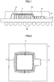
- FIG. 1 is an internal a see-through side view of a ball-grid array (BGA) type semiconductor device according to the first embodiment of the present invention.
- FIG. 2 is a see-through plan of the semiconductor device shown in FIG. 1.
- FIG. 3 is a plan view showing a structure of bonding-wires in the semiconductor device shown in FIG. 1.
- BGA ball-grid array
- the semiconductor device comprises a substrate 2, a semiconductor element 4 mounted on the substrate 2 and an impedance-matched substrate 6 mounted on the substrate 2.
- the semiconductor element 4 and the impedance-matched substrate 6 are wire-bonded to electrodes 2a (refer to FIG. 3) of the substrate 2, and those are entirely encapsulated by a seal resin 8 on the substrate 2.
- electrodes 2a (refer to FIG. 3) of the substrate 2, and those are entirely encapsulated by a seal resin 8 on the substrate 2.
- solder balls 10 Provided on the backside of the substrate 2 are solder balls 10 which serve as external connection terminals.
- Electrodes (first electrodes) 4a are arranged along four sides of the semiconductor element 4, and a pitch of the electrodes 4a is a fine pitch.
- the substrate 2 is a low-cost substrate, and a pitch of the electrodes is larger than the electrode pitch of the semiconductor element 4. Therefore, a distance between adjacent wires among the bonding-wires (first metal wires) 12 that connect the electrode 4a of a semiconductor element 4 to the electrodes 2a of the substrate 2 gradually increases from the semiconductor 4 side to the substrate 2 side, as shown in FIG. 2.
- the semiconductor device 4 has electrodes (second electrodes) 4b corresponding to, for example, high-speed signal lines in addition to the electrodes (first electrodes) 4a connected to the electrode 2a of the substrate 2 by the bonding-wires 12.
- the electrodes 4b are connected to electrodes 6b formed on the impedance-matched substrate 6 through bonding-wires (second metal wires) 14.
- an impedance of the high-speed signal line needs to be adjusted with respect to a path between the internal wiring of the semiconductor element 4 to the wiring of the substrate 2.
- an appropriate impedance for example 100 ⁇
- wiring is previously formed in the impedance-matched substrate 6 so that a predetermined impedance is attained (refer to FIG. 4).
- the impedance-matched substrate 6 is provided at a position close to a portion where the electrodes 4b corresponding to the high-speed lines 14 of the semiconductor element 4. That is, one side of the impedance-matched substrate 6 having a generally quadrilateral shape is positioned close to one side (side where the electrodes for high-speed signal lines are arranged) of the semiconductor element 4.
- the electrodes 4b corresponding to the high-speed signal lines of the semiconductor element 4 are connected to the electrodes (first electrodes) 6a of the impedance-matched substrate 6 by through he bonding wires 14.
- the pitch of the electrode 6a of the impedance-matched substrate 6 connected by the bonding-wires 14 is set to be equal to the pitch of the electrodes 4b of the semiconductor element 4 so that the bonding wires 14 extend parallel to each other. Moreover, since the impedance-matched substrate 6 is positioned close to the semiconductor element 4, the bonding-wires 14 can be much shorter than the bonding-wires 12, which enables to minimize the impedance of the bonding-wires 12.
- the electrodes 6b provided along other three sides of the impedance-matched substrate 6 are arranged at an electrode pitch equal to the pitch of the electrodes 2a of the substrate. Therefore, the electrodes 6b of the impedance-matched substrate 6 are connected to the electrodes 2a of the substrate 2 by bonding-wires (third metal wires) 16 parallel to each other.
- FIG. 4 is a perspective view of the impedance-matched substrate 6 and the semiconductor element 4, wherein wires 6c formed on the substrate are shown.
- the impedance-matched substrate 6 can be any substrate made of a material such as an organic substrate, a glass substrate or a metal substrate if the substrate is thinner than the semiconductor element 4 and wiring can be formed thereon.
- a description will be given of a case where a copper substrate is used.
- a substrate formed of a conductive material such as a copper substrate
- a portion of the substrate other than wirings can be at a power supply potential or a grounding potential.
- the electrodes formed on the impedance-matched substrate 6 can be formed as a part of the pattern wiring, and there is no need to separate the electrodes from the pattern wiring.
- an insulating layer 6d which is slightly larger than pattern wire 6c, is formed on the copper substrate, and, then, the pattern wire 6c is formed on the insulating layer 6d.
- An end (corresponding to the electrode 6a) of each pattern wire 6c is located near the side facing the semiconductor element 4, and an opposite end (corresponding to the electrode 6b) is located near other three sides.
- Each pattern wire 6c is formed with predetermined length and width so as to have a desired impedance (for example, 100 ⁇ ).
- the impedance of the pattern wire can be made smaller than an impedance of a bonding-wire, and can be set to a desired value with higher accuracy. Therefore, the electrode 4bs of the semiconductor element 4 are connectable with the electrode 2b of the substrate 2 through the impedance with accuracy higher than the bonding-wires 12. It should be noted that both the bonding-wires 14 and bonding wires 16 are sufficiently shorter than the bonding-wires 12, which gives less influence of impedance.
- the portion of the surface of the impedance-matched substrate 6 where no pattern wire is provided is set to a power supply potential or a grounding potential so as to serves as a shield wiring or a shield plane.
- the thickness of the impedance-matched substrate 6 is preferably equal to or smaller than the thickness of the semiconductor element 4. This is because the sum total of the length of the bonding-wire 14 and the bonding-wire 16 becomes too large if the thickness of the impedance-matched substrate 6 is larger than the thickness of the semiconductor element 4. Moreover, it is more preferable that the thickness of the impedance-matched substrate 6 is one half of the thickness of the semiconductor element 4.
- differences in height between the bonding surfaces to which the bonding-wires 14 and the bonding-wires 16 are bonded (a difference in height between the surface of the semiconductor element and the surface of the impedance-matched substrate 6 and a difference in height between the surface of the impedance-matched substrate 6 and the surface of the substrate 2) become equal to each other, which provides an advantage in that the bonding can be performed by the same wire-bonding apparatus.
- An impedance-matched substrate 6A shown in FIG. 5 is provided with notches 6Aa at portions where the electrodes 6b are provided.
- the surface of the substrate 2, which is exposed by the notches 6Aa, is provided with electrodes 2a (not shown in the figure), and the electrodes 6b are connected to the electrodes 2a. Therefore, the bonding-wires 16 extend on the inner side of the notches 6Aa.
- the impedance-matched substrate 6A is a copper substrate, and the inner side of each notch 6Aa is surrounded by the copper surfaces in three directions, which is a state where the bonding wires 16 are shielded by the inner surfaces of each notch 6Aa. Therefore, a noise-reducing effect can be obtained by shielding the bonding wires 16 to which a noise tends to enter.
- the impedance-matched-substrate 6A is formed of a material other than a conductive material like the copper substrate, the same shield effect can be acquired by plating a conductive material such as a copper plating on the inner surfaces of the notches.
- the bonding-wires 14 connect between the electrode 4b of the semiconductor element 4 and the electrode 6a of the impedance-matched substrates 6 or 6A.
- the electrodes 4b of the semiconductor element 4 are set as a primary side of bonding and the electrodes 6a of the impedance-matched substrates 6 or 6A, which are at a position lower than the electrodes 4a, are set as a secondary side of bonding.
- a ball portion formed at the end of a wire is bonded. Since the size of the ball can be made smaller than the pitch of the electrodes 4b of the semiconductor element 4, the bonding portion on the primary side does not give influence to wire-bonding.
- the wire is pulled apart while being pressed against the electrode 6a.
- the crushed wire spreads in left and right directions and extend to the adjacent electrodes 6a. That is, since a portion referred to as a fish tail is formed on the secondary side of bonding, the interval of the electrodes 6a must be increased in consideration of the fish tail.
- the pitch of the electrodes 6a of the impedance-matched substrates 6 or 6A is made equal to the pitch of the electrodes 4b of the semiconductor element 4 so as to cause the bonding-wires 14 parallel to each other, and there is no need to reduce the interval of the electrodes 6a.
- a projection electrode 18 on each electrode 6a, as shown in FIG. 6, so that the fish tail does not protrude from a top surface of the projection electrode 18.
- the projection electrode 18 can be formed using, for example, a stud bump, a plating bump, etc.
- FIG. 7 is a plan of an impedance-matched substrate 6B which is provided with signal wires serving as differential pairs.
- the impedance-matched substrate 6B has a fundamental structure the same as that of the impedance-matched substrate 6, each two pattern wires 6c are formed to make a pair and both the pattern wires 6c that make pair are formed with the same width and length.
- a pair of pattern wires 6c corresponds to signal wires, and the bonding-wires 14 and 16 connected to the pattern wires 6c are given a sign S.
- a sign G is given to the bonding-wires 14 and 16 used as grounding wiring.
- a pair of bonding-wires 14 and 16 (wires to which the sign S is given) connected to a pair of pattern wires 6c are interposed between the bonding-wires 14 and 16 that serve as grounding wires so as to be shielded by the bonding-wires 14 and 16.
- the copper substrate is used in the present embodiment, and, thus, electrodes for the bonding-wires 14 and 16 that serves as grounding wires are not provided, and the bonding-wires 14 and 16 serving as grounding wires are bonded directly to the copper substrate. Therefore, the copper substrate itself is set to a grounding potential.
- the winding pattern wire 6c in each of the upper and lower pairs of pattern wires is provided with the winding portion so that a length of the winding pattern wire 6c is equal to the other pattern wire 6c of the pair.
- Notches shown in FIG. 5 may be provided to an impedance-matched substrate 6C shown in FIG. 7.
- FIG. 8 is a plan view showing the impedance-matched substrate 6C provided with notches 6Ca.
- the notches 6Ca provide the same effects as the notches 6Aa of the impedance-matched substrate 6A shown in FIG. 5.
- the bonding-wires 16 for signal wiring (wires to which the sign S is given) are interposed between the inner surfaces of the notches 6Ca, and there is no need to provide the bonding-wires for grounding wiring.
- FIG. 9 is a see-through plan view of a semiconductor device according to the second embodiment of the present invention.
- FIG. 10 is a plan view showing a bonding structure in the semiconductor device shown in FIG. 9. It should be noted that, in FIGS. 9 and 10, parts that are the same as the parts shown in FIGS. 1 through FIG. 3 are given the same reference numerals, and descriptions thereof will be omitted.
- the structure of the semiconductor device according to the second embodiment of the prevent invention is the same as the semiconductor device according to the above-mentioned first embodiment except for an impedance-matched substrate 6D having a triangular shape. That is, as shown in FIG. 9, the semiconductor device according to the second embodiment has a triangular shape of which one side is located close to one side of the semiconductor element 4. In this case, as shown in FIG. 10, the electrodes 6a connected to the electrodes 4b of the semiconductor element are provided along the side facing the semiconductor element 4 of the impedance-matched substrate 6D, and the provides electrodes 6b connected to the electrodes 2a of the substrate 2 are provided along other two sides of the impedance-matched substrate 6D.
- the bonding-wires 16 extending from the impedance-matched substrate 6D can be stretched in a direction of separating away from the semiconductor element 4. Accordingly, the wiring path in the impedance-matched substrate 6D can be a smooth path, and, a connection to the wiring in the substrate 2 after extending from the impedance-matched substrate 6D can be made smooth.
- the bonding-wires 120 that connect electrodes 4a of the semiconductor element 4 to the electrodes 2a of the substrate 2 can be stretched to pass above the impedance-matched substrate 6D. Thereby, a degree of freedom in providing the bonding-wires can be increased, and a degree of freedom in the position of the electrodes 2a of the substrate 2 can also be increase.
- FIG. 11 is a plan view of a variation of the impedance-matched substrate 6D shown in FIG. 10.
- An impedance-matched substrate 6E shown in FIG. 11 has a shape in which corners of a triangle are cut off.
- the portions of the corners of the triangular angle cannot be provided with wiring, which are useless portions. For this reason, the corners of the triangular shape are cut off like the impedance-matched substrate 6E so as to miniaturize the impedance-matched substrate.
- the impedance-matched substrate is not limited to the triangular shape of the quadrangle shape, and may be a polygonal shape or a polygonal shape of which corners are cut off. Moreover, a shape having bowed sides may be used other than shapes having straight sides.
- FIG. 12 is a plan view shown in an example in which the two impedance-matched substrate 6D shown in FIG. 10 are provided with respect to one semiconductor element 4.
- a semiconductor element has many signal lines that require impedance-matching, there may be a case where a single impedance-matched substrate is insufficient.
- the impedance-matched substrate according to the present invention is not limited to one with respect a single semiconductor element, and a plurality of impedance-matched substrates may be provided with respect to a single semiconductor element.
Landscapes
- Wire Bonding (AREA)
- Waveguides (AREA)
Applications Claiming Priority (2)
| Application Number | Priority Date | Filing Date | Title |
|---|---|---|---|
| JP2004164858A JP4083142B2 (ja) | 2004-06-02 | 2004-06-02 | 半導体装置 |
| JP2004164858 | 2004-06-02 |
Publications (2)
| Publication Number | Publication Date |
|---|---|
| EP1605506A2 true EP1605506A2 (de) | 2005-12-14 |
| EP1605506A3 EP1605506A3 (de) | 2007-12-19 |
Family
ID=34981885
Family Applications (1)
| Application Number | Title | Priority Date | Filing Date |
|---|---|---|---|
| EP20040256218 Withdrawn EP1605506A3 (de) | 2004-06-02 | 2004-10-08 | Halbleiteranordnung |
Country Status (6)
| Country | Link |
|---|---|
| US (1) | US7042102B2 (de) |
| EP (1) | EP1605506A3 (de) |
| JP (1) | JP4083142B2 (de) |
| KR (1) | KR100671808B1 (de) |
| CN (1) | CN1332440C (de) |
| TW (1) | TWI252566B (de) |
Families Citing this family (8)
| Publication number | Priority date | Publication date | Assignee | Title |
|---|---|---|---|---|
| US7341887B2 (en) * | 2004-10-29 | 2008-03-11 | Intel Corporation | Integrated circuit die configuration for packaging |
| JP5562898B2 (ja) * | 2011-04-28 | 2014-07-30 | 株式会社東芝 | 半導体装置およびその製造方法 |
| US8723337B2 (en) * | 2011-07-14 | 2014-05-13 | Texas Instruments Incorporated | Structure for high-speed signal integrity in semiconductor package with single-metal-layer substrate |
| US8949761B2 (en) * | 2012-11-30 | 2015-02-03 | International Business Machines Corporation | Techniques for routing signal wires in an integrated circuit design |
| CN103674496B (zh) | 2013-12-23 | 2016-05-25 | 京东方科技集团股份有限公司 | 光源发光特性检测装置 |
| WO2019156051A1 (ja) * | 2018-02-08 | 2019-08-15 | 株式会社村田製作所 | 高周波モジュール |
| CN114446924A (zh) * | 2022-01-25 | 2022-05-06 | 杭州云合智网技术有限公司 | 半导体结构及芯片封装方法 |
| WO2025144556A1 (en) * | 2023-12-29 | 2025-07-03 | Littelfuse, Inc. | Power semiconductor module having trapezoidal substrate |
Family Cites Families (25)
| Publication number | Priority date | Publication date | Assignee | Title |
|---|---|---|---|---|
| JPS59110127A (ja) * | 1982-12-15 | 1984-06-26 | Matsushita Electric Works Ltd | ヒ−トシンク |
| JPS62125638A (ja) * | 1985-11-26 | 1987-06-06 | Nec Corp | 混成集積回路 |
| US5077595A (en) * | 1990-01-25 | 1991-12-31 | Mitsubishi Denki Kabushiki Kaisha | Semiconductor device |
| DE4217289C2 (de) * | 1992-05-25 | 1996-08-29 | Mannesmann Ag | Fluidgekühlte Leistungstransistoranordnung |
| JPH066151A (ja) | 1992-06-17 | 1994-01-14 | Fujitsu Ltd | 高周波半導体装置 |
| US5340772A (en) * | 1992-07-17 | 1994-08-23 | Lsi Logic Corporation | Method of increasing the layout efficiency of dies on a wafer and increasing the ratio of I/O area to active area per die |
| JPH0637202A (ja) * | 1992-07-20 | 1994-02-10 | Mitsubishi Electric Corp | マイクロ波ic用パッケージ |
| JPH06334113A (ja) * | 1993-05-21 | 1994-12-02 | Sony Corp | マルチチップモジュール |
| JP2944403B2 (ja) * | 1993-12-24 | 1999-09-06 | 日本電気株式会社 | 半導体装置 |
| USRE37081E1 (en) * | 1994-05-27 | 2001-03-06 | Steen M. Eriksen | Backpack vacuum cleaner |
| JP3462270B2 (ja) * | 1994-08-19 | 2003-11-05 | 富士通株式会社 | 半導体装置 |
| JPH0936159A (ja) * | 1995-07-17 | 1997-02-07 | Toshiba Corp | 半導体装置及びその封止方法 |
| JP3489926B2 (ja) * | 1995-11-28 | 2004-01-26 | 三菱電機株式会社 | 高周波回路装置 |
| US6049126A (en) * | 1995-12-14 | 2000-04-11 | Nec Corporation | Semiconductor package and amplifier employing the same |
| US5789816A (en) * | 1996-10-04 | 1998-08-04 | United Microelectronics Corporation | Multiple-chip integrated circuit package including a dummy chip |
| JP2933041B2 (ja) | 1996-12-18 | 1999-08-09 | 日本電気株式会社 | 半導体装置 |
| JP3638749B2 (ja) | 1997-02-28 | 2005-04-13 | 新潟精密株式会社 | メモリモジュール |
| JP3520973B2 (ja) * | 1999-11-30 | 2004-04-19 | Necエレクトロニクス株式会社 | 半導体装置 |
| JP4439090B2 (ja) * | 2000-07-26 | 2010-03-24 | 日本テキサス・インスツルメンツ株式会社 | 半導体装置及びその製造方法 |
| JP2003078304A (ja) * | 2001-08-30 | 2003-03-14 | Murata Mfg Co Ltd | 電子モジュールおよびそれを用いた通信機モジュール |
| DE10152652A1 (de) * | 2001-10-16 | 2003-04-30 | Infineon Technologies Ag | Hochfrequenzleistungsverstärker mit integrierter passiver Anpassungsschaltung |
| US6614308B2 (en) * | 2001-10-22 | 2003-09-02 | Infineon Technologies Ag | Multi-stage, high frequency, high power signal amplifier |
| JP4003579B2 (ja) * | 2002-08-09 | 2007-11-07 | 住友電気工業株式会社 | コプレーナ線路構造、伝送モジュール用パッケージ及び伝送モジュール |
| JP2004112178A (ja) * | 2002-09-17 | 2004-04-08 | Fujitsu Quantum Devices Ltd | 伝送線路及びそれを有する装置 |
| US6982483B2 (en) * | 2003-05-30 | 2006-01-03 | Freescale Semiconductor, Inc. | High impedance radio frequency power plastic package |
-
2004
- 2004-06-02 JP JP2004164858A patent/JP4083142B2/ja not_active Expired - Fee Related
- 2004-10-08 EP EP20040256218 patent/EP1605506A3/de not_active Withdrawn
- 2004-10-25 US US10/971,692 patent/US7042102B2/en not_active Expired - Fee Related
- 2004-10-25 KR KR20040085180A patent/KR100671808B1/ko not_active Expired - Fee Related
- 2004-10-26 TW TW93132365A patent/TWI252566B/zh not_active IP Right Cessation
- 2004-10-29 CN CNB2004100880277A patent/CN1332440C/zh not_active Expired - Fee Related
Also Published As
| Publication number | Publication date |
|---|---|
| CN1332440C (zh) | 2007-08-15 |
| EP1605506A3 (de) | 2007-12-19 |
| CN1705102A (zh) | 2005-12-07 |
| KR20050115439A (ko) | 2005-12-07 |
| US20050269701A1 (en) | 2005-12-08 |
| TW200541023A (en) | 2005-12-16 |
| US7042102B2 (en) | 2006-05-09 |
| TWI252566B (en) | 2006-04-01 |
| JP4083142B2 (ja) | 2008-04-30 |
| KR100671808B1 (ko) | 2007-01-19 |
| JP2005347489A (ja) | 2005-12-15 |
Similar Documents
| Publication | Publication Date | Title |
|---|---|---|
| JP2679965B2 (ja) | 半導体チップパッケージ | |
| US5581122A (en) | Packaging assembly with consolidated common voltage connections for integrated circuits | |
| US7514789B1 (en) | Ball grid array package-to-board interconnect co-design apparatus | |
| US8039320B2 (en) | Optimized circuit design layout for high performance ball grid array packages | |
| US6593647B2 (en) | Semiconductor device | |
| US8637975B1 (en) | Semiconductor device having lead wires connecting bonding pads formed on opposite sides of a core region forming a shield area | |
| JPH04137655A (ja) | Icパッケージ | |
| US7042102B2 (en) | Semiconductor device | |
| US5726860A (en) | Method and apparatus to reduce cavity size and the bondwire length in three tier PGA packages by interdigitating the VCC/VSS | |
| EP0835047A2 (de) | RF-betriebene Halbleiteranordnung | |
| KR950014677B1 (ko) | Ic 실장장치 | |
| US9905517B2 (en) | Semiconductor device | |
| EP1519413A1 (de) | Anordnung der Kontaktlöcher für Schichtübergänge in flexiblen Schaltkreisen mit dichten Kugelmatrixpackungen | |
| US11211349B2 (en) | Semiconductor device including a plurality of bonding pads | |
| JP2845218B2 (ja) | 電子部品の実装構造およびその製造方法 | |
| JP2001352000A (ja) | インターポーザを使用した高周波用半導体装置 | |
| US20040227226A1 (en) | Structure of multi-tier wire bonding for high frequency integrated circuits and method of layout for the same | |
| US6646343B1 (en) | Matched impedance bonding technique in high-speed integrated circuits | |
| KR100374242B1 (ko) | 반도체 장치 | |
| JP2011216522A (ja) | 半導体装置 | |
| JP2000269382A (ja) | 半導体装置及び半導体チップの実装方法 | |
| JPS6348129Y2 (de) | ||
| JPH08167818A (ja) | 高周波装置 | |
| JPH0352260A (ja) | 電子回路装置 | |
| JPH04352463A (ja) | リードフレームおよびこれを用いた半導体装置 |
Legal Events
| Date | Code | Title | Description |
|---|---|---|---|
| PUAI | Public reference made under article 153(3) epc to a published international application that has entered the european phase |
Free format text: ORIGINAL CODE: 0009012 |
|
| AK | Designated contracting states |
Kind code of ref document: A2 Designated state(s): AT BE BG CH CY CZ DE DK EE ES FI FR GB GR HU IE IT LI LU MC NL PL PT RO SE SI SK TR |
|
| AX | Request for extension of the european patent |
Extension state: AL HR LT LV MK |
|
| PUAL | Search report despatched |
Free format text: ORIGINAL CODE: 0009013 |
|
| AK | Designated contracting states |
Kind code of ref document: A3 Designated state(s): AT BE BG CH CY CZ DE DK EE ES FI FR GB GR HU IE IT LI LU MC NL PL PT RO SE SI SK TR |
|
| AX | Request for extension of the european patent |
Extension state: AL HR LT LV MK |
|
| 17P | Request for examination filed |
Effective date: 20080616 |
|
| AKX | Designation fees paid |
Designated state(s): DE FR GB |
|
| RAP1 | Party data changed (applicant data changed or rights of an application transferred) |
Owner name: FUJITSU MICROELECTRONICS LIMITED |
|
| 17Q | First examination report despatched |
Effective date: 20090922 |
|
| RAP1 | Party data changed (applicant data changed or rights of an application transferred) |
Owner name: FUJITSU SEMICONDUCTOR LIMITED |
|
| RAP1 | Party data changed (applicant data changed or rights of an application transferred) |
Owner name: SOCIONEXT INC. |
|
| STAA | Information on the status of an ep patent application or granted ep patent |
Free format text: STATUS: EXAMINATION IS IN PROGRESS |
|
| STAA | Information on the status of an ep patent application or granted ep patent |
Free format text: STATUS: THE APPLICATION IS DEEMED TO BE WITHDRAWN |
|
| 18D | Application deemed to be withdrawn |
Effective date: 20180501 |
|
| RIC1 | Information provided on ipc code assigned before grant |
Ipc: H01L 23/552 20060101ALI20051026BHEP Ipc: H01L 23/66 20060101AFI20051026BHEP Ipc: H01L 23/498 20060101ALI20051026BHEP Ipc: H01L 21/607 20060101ALI20051026BHEP |