EP1619528A1 - Halbleitervorrichtung mit einem Halterungsbauteil für optischen Wellenleiter und Verfahren zu deren Herstellung - Google Patents
Halbleitervorrichtung mit einem Halterungsbauteil für optischen Wellenleiter und Verfahren zu deren Herstellung Download PDFInfo
- Publication number
- EP1619528A1 EP1619528A1 EP05254524A EP05254524A EP1619528A1 EP 1619528 A1 EP1619528 A1 EP 1619528A1 EP 05254524 A EP05254524 A EP 05254524A EP 05254524 A EP05254524 A EP 05254524A EP 1619528 A1 EP1619528 A1 EP 1619528A1
- Authority
- EP
- European Patent Office
- Prior art keywords
- optical waveguide
- base material
- substrate
- hole
- optic fiber
- Prior art date
- Legal status (The legal status is an assumption and is not a legal conclusion. Google has not performed a legal analysis and makes no representation as to the accuracy of the status listed.)
- Granted
Links
Images




Classifications
-
- G—PHYSICS
- G02—OPTICS
- G02B—OPTICAL ELEMENTS, SYSTEMS OR APPARATUS
- G02B6/00—Light guides; Structural details of arrangements comprising light guides and other optical elements, e.g. couplings
- G02B6/24—Coupling light guides
- G02B6/42—Coupling light guides with opto-electronic elements
- G02B6/4201—Packages, e.g. shape, construction, internal or external details
- G02B6/4219—Mechanical fixtures for holding or positioning the elements relative to each other in the couplings; Alignment methods for the elements, e.g. measuring or observing methods especially used therefor
- G02B6/422—Active alignment, i.e. moving the elements in response to the detected degree of coupling or position of the elements
-
- G—PHYSICS
- G02—OPTICS
- G02B—OPTICAL ELEMENTS, SYSTEMS OR APPARATUS
- G02B6/00—Light guides; Structural details of arrangements comprising light guides and other optical elements, e.g. couplings
- G02B6/24—Coupling light guides
- G02B6/42—Coupling light guides with opto-electronic elements
- G02B6/4201—Packages, e.g. shape, construction, internal or external details
- G02B6/4204—Packages, e.g. shape, construction, internal or external details the coupling comprising intermediate optical elements, e.g. lenses, holograms
- G02B6/421—Packages, e.g. shape, construction, internal or external details the coupling comprising intermediate optical elements, e.g. lenses, holograms the intermediate optical component consisting of a short length of fibre, e.g. fibre stub
-
- G—PHYSICS
- G02—OPTICS
- G02B—OPTICAL ELEMENTS, SYSTEMS OR APPARATUS
- G02B6/00—Light guides; Structural details of arrangements comprising light guides and other optical elements, e.g. couplings
- G02B6/24—Coupling light guides
- G02B6/42—Coupling light guides with opto-electronic elements
- G02B6/4201—Packages, e.g. shape, construction, internal or external details
- G02B6/4249—Packages, e.g. shape, construction, internal or external details comprising arrays of active devices and fibres
-
- H—ELECTRICITY
- H10—SEMICONDUCTOR DEVICES; ELECTRIC SOLID-STATE DEVICES NOT OTHERWISE PROVIDED FOR
- H10W—GENERIC PACKAGES, INTERCONNECTIONS, CONNECTORS OR OTHER CONSTRUCTIONAL DETAILS OF DEVICES COVERED BY CLASS H10
- H10W90/00—Package configurations
- H10W90/701—Package configurations characterised by the relative positions of pads or connectors relative to package parts
- H10W90/721—Package configurations characterised by the relative positions of pads or connectors relative to package parts of bump connectors
- H10W90/724—Package configurations characterised by the relative positions of pads or connectors relative to package parts of bump connectors between a chip and a stacked insulating package substrate, interposer or RDL
Definitions
- the present invention generally relates to an optical waveguide mounting member, a substrate, a semiconductor device, a method of manufacturing an optical waveguide mounting member, and a method of manufacturing a substrate, and more particularly to an optical waveguide mounting member, a substrate, a semiconductor device, a method of manufacturing an optical waveguide mounting member, and a method of manufacturing a substrate for transmitting optic signals to an optical element via an optic fiber.
- optical communication in optical communication, electric signals are converted to optical signals, the optical signals are transmitted through an optic fiber, and the received optical signals are converted to electric signals by an optical element having a light emission and/or light reception part (hereinafter referred to as "light emission/reception part).
- the light emission/reception part is a part for transmitting and receiving optical signals.
- the optical element includes, for example, a vertical cavity surface emitting laser (VCSEL), a photodiode (hereinafter referred to as "PD”), and a laser diode (hereinafter referred to as "LD").
- VCSEL vertical cavity surface emitting laser
- PD photodiode
- LD laser diode
- a core part of an optic fiber which is mounted in a through-hole penetrating the substrate, is positioned in a manner facing the light emission/reception part of the optical element.
- FIG.1 is a cross-sectional view showing the semiconductor device 10 having the optical elements 15, 16.
- the semiconductor device 10 mainly includes a substrate 20, optical elements 15, 16 having light emission/reception parts 15A, 16A, an optical waveguide 17, and mirrors 21, 22.
- the substrate 20 mainly includes a resin base material 11, through-holes 12a, 12b, an optic fibers 13, 14, and pads (not shown), wirings (not shown), and solder resist that covers the wirings (not shown).
- the pads, wirings, and the solder resist are provided on a plane 11A of the resin base material 11.
- the pads are provided for connecting to solder balls 24, 25 of the optical elements 15, 16.
- the pads are provided in an exposed state (i.e. not covered by the solder resist).
- the through-holes 12a, 12b are formed in the resin base material 11 in a manner penetrating the resin base material 11 by irradiating a laser (e.g. a YAG laser, a CO 2 laser, an excimer laser) to the resin base material 11.
- a laser e.g. a YAG laser, a CO 2 laser, an excimer laser
- the through-hole 12a is provided with an optic fiber 13
- the through-hole 12b is provided with an optic fiber 14.
- the optic fibers 13, 14 include core parts 13a, 14a, and clad parts 13b, 14b that cover the core parts 13a, 14a.
- Optical signals are transmitted by the core parts 13a, 14a.
- the optical element 15 is mounted on the substrate 20 in a manner that the light emission/reception part 15A of the optical element 15 faces the core part 13a of the optic fiber 13.
- the optical element 16, which is provided with the solder ball 25, has the solder ball 25 connected to the pad (not shown) of the substrate 20. Accordingly, optical element 16 is electrically connected to the substrate 20.
- the optical element 16 is mounted on the substrate 20 in a manner that the light emission/reception part 16A of the optical element 16 faces the core part 14a of the optic fiber 14.
- the mirror 21 is provided at an end part 13B of the optic fiber 13 and the mirror 22 is provided at an end part 14B of the optic fiber 14.
- the mirrors 21, 22 are provided for enabling optical transmission between the optical waveguide 17 and the optic fibers 13, 14.
- the optical waveguide 17 includes a core part 18 and a clad part 19 that covers the periphery of the core part 18.
- the optical waveguide 17 is provided between the mirror 21 and the mirror 22 for allowing optical signals to be transmitted therethrough (See, for example, Japanese Laid-Open Patent Application No.2004-54003).
- the semiconductor 10 it is desirable to reduce deviation between the positions of the core parts 13a, 14a of the optic fibers 13, 14 (mounted in the through-holes 12a, 12b) and the positions of the corresponding light emission/reception parts 15A, 16A facing the core parts 13a, 13b, so that transmission loss between the optic fibers 13, 14 and the light emission/reception parts 15A, 16A can be reduced.
- Fig.2 is a plane view of the substrate 20 having the optic fiber 13 mounted in the through-hole 12a.
- L1 indicates a space formed between the wall of the through-hole 12a (12b) having a diameter R2 and an outer diameter R1 of the optical fiber 13 (14) (hereinafter referred to as "space L1").
- space L1 the through-holes 12a, 12b corresponding to the optic fibers 13, 14 are formed by irradiating a laser (e.g.
- a large space L1 (e.g. approximately 10 ⁇ m) is provided between the wall of the through-hole 12a, 12b having diameter R2 and the optic fiber 13, 14 having outer diameter R1 for enabling attachment between the optic fibers 13, 14 and the through-holes 12a, 12b
- the position of the core parts 13a, 14a of the optic fibers 13, 14 attached to the through-holes 12a, 12b tends to deviate from the position of the corresponding light emission/reception parts 15A, 16A. This makes it difficult to reduce transmission loss of optical signals.
- the resin base material 11 in which the through-holes 12a, 12b are formed may change the position of the optic fibers 13, 14 attached to the through-holes 12a, 12b in a case where thermal deformation (thermal contraction or thermal expansion) of the resin base material 11 occurs when the temperature of the substrate 20 changes. This results in an increase of transmission loss of optical signals.
- Fig.3 shows an example a substrate having optic fibers in a state before being subjected to a polishing process.
- letters "A” and “B” each indicate a part of an optic fiber 36 protruding from a resin base material 331 (hereinafter referred to as “protruding part A” and “protruding part B”).
- the process of polishing the protruding parts A, B is performed after pads 32, 37, wirings 33, 38, and solder resist 34, 39 are formed on both sides of the resin substrate 31.
- the presence of the pads 32, 37, wirings 33, 38, and solder resist 34, 39 formed on both sides of the resin substrate 31 may obstruct the process of polishing the protruding parts A, B. Therefore, it is difficult to polish the protruding parts A, B of the optic fiber 36 with satisfactory precision in a direction perpendicularly intersecting with a plane direction of the resin substrate 31.
- the invention provides an optical waveguide mounting member for mounting to a substrate, the optical waveguide mounting member including: an optical waveguide for transmitting optical signals therethrough; and an optical waveguide mounting base material having a through-hole to which the optical waveguide is mounted; wherein the optical waveguide mounting base material is formed of silicon.
- the through-hole may be an anisotropic-etched hole.
- the present invention provides a substrate including: the optical waveguide mounting member according to the embodiment of the present invention; and a substrate main body having a perforated part; wherein the optical waveguide mounting member is mounted in the perforated part of the substrate main body.
- the present invention provides a semiconductor device including: an optical element having a light emission/reception part; and the substrate according to the embodiment of the present invention; wherein the optical waveguide of the substrate is positioned opposite to the light emission/reception part of the optical element.
- the present invention provides a method of manufacturing one or more optical waveguide mounting members for mounting to a substrate, the optical waveguide mounting member having an optical waveguide for transmitting optical signals therethrough and an optical waveguide mounting base material having a through-hole to which the optical waveguide is mounted, the method including the steps of: a) forming the optical waveguide mounting base material with a silicon material; and b) forming the through-hole of the optical waveguide mounting base material by anisotropic etching.
- the method may further include the steps of: c) mounting the optical waveguide in the through-hole; and d) polishing a protruding part of the optical waveguide protruding from the through-hole.
- the present invention provides a method of manufacturing a substrate to which an optical waveguide mounting member is mounted, the optical waveguide mounting member having an optical waveguide for transmitting optical signals therethrough and an optical waveguide mounting base material including a through-hole to which the optical waveguide is mounted, the method including the steps of: a) forming the optical waveguide mounting base material with a silicon material; b) forming the through-hole of the optical waveguide mounting base material by anisotropic etching; c) mounting the optical waveguide in the through-hole; d) polishing a protruding part of the optical waveguide protruding from the through-hole; e) forming a perforated part in a substrate main body; and f) mounting the optical waveguide mounting member in the perforated part.
- FIG.4 is a cross-sectional view of the semiconductor device 50 according to the embodiment of the present invention. It is to be noted that, although there is shown in Fig.4 only a single optical element 80 mounted on a substrate 60, multiple optical elements 80 may be mounted on the substrate 60. Furthermore, in Fig.3, a plane 56A of a base material 56 indicates a plane of the base material 56 facing the side on which the optical element 80 is mounted, and a plane 56B of the base material 56 indicates a plane of the base material 56 facing the side to which a motherboard (not shown) is mounted.
- the semiconductor device 50 mainly includes the optical element 80 and the substrate 60.
- the optical element 80 is an optical element for converting optic signals to electric signals.
- the optical element 80 includes multiple light emission/reception parts 81 and solder balls 82 serving as external connection terminals.
- the light emission/reception parts 51 are provided to the optical element 80 for receiving optical signals transmitted from optic fibers 74 and/or for transmitting optical signals from the optical element 80 to the optic fibers 74.
- the optical element 80 includes, for example, a vertical cavity surface emitting laser (VCSEL), a photodiode (hereinafter referred to as “PD”), and a laser diode (hereinafter referred to as "LD").
- the solder balls 82 are provided for electrically connecting between the optical element 80 and the substrate 60.
- the optical element 80 is mounted on the substrate 60 in a manner having the light emission/reception parts 81 facing toward core parts 75 of the optic fibers 41 (mounted in an optic fiber mounting member 70 of the substrate 60, described in detail below).
- the substrate 60 mainly includes a substrate main body 55 and the optic fiber mounting member 70 which is an optical waveguide mounting member.
- the substrate 60 having the optical element 80 mounted thereto, is connected to, for example, a motherboard (not shown).
- the optic fiber mounting member 70 is adhesively fixed to a wall of a perforated part 68 of the substrate main body 55 in a manner that a plane 71B of the optic fiber mounting member 71 and the plane 56B of the substrate 56 are situated on a same plane.
- Fig.5 is a cross-sectional view of the substrate main body 55 according to the embodiment of the present invention.
- Fig.6 is a plane view of the substrate main body 55 shown in Fig.5.
- the substrate main body 55 mainly includes the base material 56, a via(s) 57, pads 59, 62, wiring 58, 63, solder resist 61, 64, an Ni/Au metal layer 66, a solder ball(s) 67, and the perforated part 68.
- the base material 56 is made of, for example, resin material.
- the base material 56 is formed with a thickness M1 of, for example, approximately 150 ⁇ m.
- the via 57 is formed in the base material 56 by perforating the base material 56.
- the perforated part 68 is formed at a center area of the base material 68.
- the optic fiber mounting member 70 having multiple optic fibers 74 mounted thereto, is mounted in the perforated part 68.
- the perforated part 68 is formed in a manner penetrating the base material 56.
- the pad 59 is provided on the plane 56A of the base material 56 and is electrically connected to the via 57.
- the pad 59 is electrically connected to the solder ball 82 of the optical element 80.
- the wiring 58 is also provided on the plane 56A of the base material 56.
- the wiring 58 is electrically connected to the pad 59.
- the solder resist 61 is applied to the plane 56A of the base material 56 in a manner covering a part of the plane 56A of the base material 56 and the wiring 58.
- the pad 62 is disposed on the plane 56B of the base material 56 and is electrically connected to the via 57.
- the wiring 63 is also provided on the plane 56B of the base material 56 and is electrically connected to the pad 62.
- the solder resist 64 is applied to the plane 56B of the base material 56 in a manner covering a part of the plane 56B of the base material 56 and the wiring 63.
- the solder ball 67 is electrically connected to the pad 62 via the Ni/Au metal layer 66.
- the solder ball 67 which is an external connection terminal, electrically connects the substrate 60 to the motherboard (not shown).
- Fig.7 is a cross-sectional view showing the optic fiber mounting member 70 according to the embodiment of the present invention.
- Fig.8 is a plane enlarged view showing a state where the optic fiber 74 is mounted in the optic fiber mounting member 70.
- a center axis C1 of the core part 75 of the optic fiber 74 is matched to a center axis C2 of a through-hole 72.
- L2 indicates a space formed between the wall of the through-hole 72 and an outer diameter R3 of the optic fiber 74 (hereinafter referred to as "space L2".
- the optic fiber mounting member 70 mainly includes: an optic fiber mounting base material 71 which is an optical waveguide mounting base material; the through-hole 72 to which the optic fiber 74 is mounted; and the optic fiber 74 which is an optical waveguide.
- the optic fiber mounting base material 71 is a base material for mounting the optic fiber 74 thereto.
- the thickness M2 of the optic fiber mounting base material 71 may be, for example, approximately 150 ⁇ m.
- silicon is employed as the material of the optic fiber mounting base material 71.
- the optic fiber 71 can be less vulnerable to thermal deformation compared to employing a conventional resin material in a case where there is a change of heat in the optic fiber mounting base material 71. Accordingly, the position of the core part 75 of the optic fiber 74 can be prevented deviating from a corresponding position of the light emission/reception part 81 of the optical element 80. Thereby, transmission loss of optical signals between the optic fiber 74 and the light emission/reception part 80 can be reduced.
- the optic fiber 74 includes the core part 75 and a clad part 76.
- the core part 75 is a part for transmitting optical signals.
- the clad part 76 is a part for protecting the core part 42 and is provided in a manner covering the core part 75.
- the optic fiber 74 is adhesively fixed to the through-hole 72 of the optic fiber mounting base material 71 via an adhesive material 78.
- the through-hole 72 is formed by using anisotropic etching so as to penetrate the optic fiber mounting base material 71 made of silicon.
- the through-hole 72 is a hole for mounting the optic fiber 72 therein.
- the anisotropic etching may be, for example, dry etching.
- the method of forming the through-hole 72 by dry-etching the optic fiber mounting base material 71 made of silicon is able to provide greater precision in the relative position between the through-hole 72 and the light emission/reception part 81 and greater precision in the size of the through-hole 72.
- the size of the through-hole 72 (to which the optic fiber 74 is to be mounted) can be reduced compared to that of the conventional through-hole. Accordingly, the space L2 between the wall of the through-hole 72 and the optic fiber 74 can be reduced, thereby allowing the wall of the through-hole 72 to secure the position of the optic fiber 74. Accordingly, the position of the optic fiber 74 can be prevented from deviating from the corresponding position of the light emission/reception part 81. Thereby, transmission loss of optical signals between the optic fiber 74 and the light emission/reception part 81 can be reduced.
- Fig.9 is a plane view of a silicon wafer for showing the area in which the optic fiber mounting member(s) 70 is formed.
- Fig.10 is a cross-sectional view of a silicon wafer along the direction of line E-E of Fig.9.
- area D in Figs.9-11 indicates the area in which the optic fiber mounting member 70 is formed.
- the area I shown in Fig.16 shows a state of the optic fiber mounting member 70 before being subjected to a dicing process.
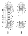
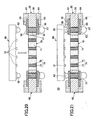
- Figs.11-21 are cross-sectional views (corresponding to the cross-section of the silicon wafer taken along line E-E of Fig.9) showing the processes of manufacturing the semiconductor device 50 according to the embodiment of the present invention (Part 1-11).
- like components are denoted with like reference numerals as of the semiconductor apparatus 50 shown in Fig.4.
- the silicon wafer 90 is used as a parent material (for example, a planar silicon material) for forming multiple optic fiber base materials 70 as a batch by performing the manufacturing method shown in Figs.11 to 21.
- a parent material for example, a planar silicon material
- a commercially available silicon wafer used for forming semiconductor chips may be employed as the silicon wafer 90.
- a commercially available silicon wafer 90, shown for example in Fig.10 may have a thickness of approximately 700-800 ⁇ m.
- a resist film 91 is formed on the silicon wafer 90.
- the resist film 91 includes aperture parts 91A for forming the through-holes 72.
- the resist film 91 is used as a mask for etching the silicon wafer 90 with an anisotropic etching method (in this example, dry-etching), and the silicon wafer 90 is etched until it is penetrated, thereby forming the through-holes 72 in the silicon wafer 90 (through-hole formation process).
- the diameter R4 of the through-hole 72 may be adaptively set according to the outer diameter R3 of the optic fiber 74 that is to be mounted in the through-hole 72.
- the diameter of the through-hole 72 may be set so that the size of the space L2 (Fig.8) is approximately 1 ⁇ m.
- the resist film 91 is removed by using a resist releasing liquid.
- the optic fibers 74 (optical waveguides) are inserted in the through-holes 72 and are attached to the walls 72A of the through-holes 72 by using an adhesive agent (optical waveguide mounting process).
- the optic fibers 74 have protruding parts G and H protruding from planes 90A and 90B of the silicon wafer 90.
- both planes 90A, 90B of the silicon wafer 90 are polished (polishing process).
- the protruding parts G, H of the optic fibers 74 are also polished. Accordingly, the optic fiber mounting base material 70 is formed with a desired thickness M2.
- the pads 59, 62, the wirings 58, 63, and the solder resist 61, 64 provided to the base material 56 can be prevented from obstructing the process of polishing the protruding parts G, H of the optic fibers 74.
- the protruding parts G, H of the optic fibers 74 can be easily polished with satisfactory precision in a direction perpendicularly intersecting with a plane direction of the optic fiber mounting members 70.
- a backside grinder for example, may be used. In a case where the backside grinder is used, the silicon wafer 90 is polished one side at a time.
- multiple optic fiber mounting members 70 with the desired thickness M2 can be formed without having to be separated from one another. Furthermore, as a result of the polishing process, one plane 71A of the optic fiber mounting base material 70 becomes aligned at the same level (same plane) with one end plane 74A of the optic fiber 74, and the other plane 71B of the optic fiber mounting base material 71 becomes aligned at the same level (same plane) with the other plane 74B of the optic fiber 74.
- the optic fiber mounting members 70 are individually cut out by dicing the silicon wafer 90, to thereby obtain multiple separated optic fiber mounting members 70 in a batch.
- the perforated part 68 is formed in the center area of the substrate main body 55 (perforated part formation process). Then, the optic fiber mounting member 70 is adhesively fixed to a wall 68A of the perforated part 68 by using an adhesive agent. Accordingly, as shown in Fig.19, the substrate 60 including the optic fiber mounting base material 71 and the substrate main body 55 is fabricated.
- the one plane 71A of the optic fiber mounting base material 71 becomes aligned at the same level (same plane) with the plane 56A of the substrate main body 55
- the other plane 71B of optic fiber mounting base material 71 becomes aligned at the same level (same plane) with the plane 56B of the substrate main body 55.
- the position between the light emission/reception parts 81 of the optical element 80 and the core parts 75 of the optic fibers 74 are adjusted by monitoring the position with a photo-detection measurement apparatus (not shown), to thereby determine an optimum position on the substrate 60 for mounting the optical element 80 (hereinafter referred to as "optimum position").
- the fabrication of the semiconductor device 50 is completed by mounting the optical element 80 on the substrate 60 in a manner that the solder balls 82 are electrically connected to the pads 59.
- the precision in the relative position between the through-holes 72 and the light emission/reception parts 81 as well as the precision in the size of the through-holes 72 can be improved. Thereby, transmission loss of optical signals between the optic fiber 74 and the light emission/reception part 81 can be reduced. Furthermore, the process of polishing the optic fiber 74 can be easily performed with satisfactory precision. Furthermore, by separately forming the optic fiber mounting member 70 and the substrate main body 55 of the substrate 60, the productivity of the substrate 60 can be improved.
- the substrate 60 according to the embodiment of the present invention may alternatively be fabricated with a multilayer wiring configuration in which multiple insulating layers and wirings are provided to the base material 56. Furthermore, components other than solder balls may be alternatively used for connecting the optical element 80 and the substrate 60.
Landscapes
- Physics & Mathematics (AREA)
- General Physics & Mathematics (AREA)
- Optics & Photonics (AREA)
- Optical Couplings Of Light Guides (AREA)
- Optical Integrated Circuits (AREA)
- Led Device Packages (AREA)
Applications Claiming Priority (1)
| Application Number | Priority Date | Filing Date | Title |
|---|---|---|---|
| JP2004216075A JP4558400B2 (ja) | 2004-07-23 | 2004-07-23 | 半導体装置 |
Publications (2)
| Publication Number | Publication Date |
|---|---|
| EP1619528A1 true EP1619528A1 (de) | 2006-01-25 |
| EP1619528B1 EP1619528B1 (de) | 2012-02-01 |
Family
ID=34982547
Family Applications (1)
| Application Number | Title | Priority Date | Filing Date |
|---|---|---|---|
| EP05254524A Ceased EP1619528B1 (de) | 2004-07-23 | 2005-07-20 | Halbleitervorrichtung mit einem Halterungsbauteil für optischen Wellenleiter und Verfahren zu deren Herstellung |
Country Status (4)
| Country | Link |
|---|---|
| US (1) | US7251391B2 (de) |
| EP (1) | EP1619528B1 (de) |
| JP (1) | JP4558400B2 (de) |
| TW (1) | TWI401480B (de) |
Cited By (1)
| Publication number | Priority date | Publication date | Assignee | Title |
|---|---|---|---|---|
| EP2613186A4 (de) * | 2010-08-31 | 2017-11-08 | Kyocera Corporation | Optische übertragungsstruktur, verfahren zu ihrer herstellung und optisches übertragungsmodul |
Families Citing this family (10)
| Publication number | Priority date | Publication date | Assignee | Title |
|---|---|---|---|---|
| JP5012447B2 (ja) * | 2007-11-20 | 2012-08-29 | 住友電気工業株式会社 | 光フェルールおよび光モジュール |
| KR101262909B1 (ko) * | 2008-04-26 | 2013-05-09 | 광주과학기술원 | 광연결 구조물 및 그 제조방법 |
| US8705906B2 (en) * | 2009-04-23 | 2014-04-22 | Korea Electronics Technology Institute | Photoelectric conversion module |
| US8390083B2 (en) * | 2009-09-04 | 2013-03-05 | Analog Devices, Inc. | System with recessed sensing or processing elements |
| JP4969711B2 (ja) | 2010-08-31 | 2012-07-04 | 京セラ株式会社 | 光伝送体およびその製造方法、ならびに光伝送モジュール |
| WO2012051340A1 (en) | 2010-10-12 | 2012-04-19 | Analog Devices, Inc. | Microphone package with embedded asic |
| CN104576883B (zh) | 2013-10-29 | 2018-11-16 | 普因特工程有限公司 | 芯片安装用阵列基板及其制造方法 |
| US9666558B2 (en) | 2015-06-29 | 2017-05-30 | Point Engineering Co., Ltd. | Substrate for mounting a chip and chip package using the substrate |
| US9899355B2 (en) * | 2015-09-30 | 2018-02-20 | Taiwan Semiconductor Manufacturing Co., Ltd. | Three-dimensional integrated circuit structure |
| US11262500B2 (en) * | 2019-12-02 | 2022-03-01 | Renesas Electronics Corporation | Semiconductor device and including an optical waveguide and method of manufacturing the same |
Citations (14)
| Publication number | Priority date | Publication date | Assignee | Title |
|---|---|---|---|---|
| US5371822A (en) * | 1992-06-09 | 1994-12-06 | Digital Equipment Corporation | Method of packaging and assembling opto-electronic integrated circuits |
| JP2000321469A (ja) * | 1999-05-12 | 2000-11-24 | Matsushita Electric Ind Co Ltd | 光結合装置とその製造方法および光ファイバモジュール |
| US6181864B1 (en) * | 1997-08-14 | 2001-01-30 | Samsung Electronics Co., Ltd. | Optical fiber array module using soldering and fabrication method thereof |
| US20020015556A1 (en) * | 2000-06-19 | 2002-02-07 | Steinberg Dan A. | Method of fabricating an optical fiber array using photosensitive material |
| US20020028057A1 (en) * | 2000-06-19 | 2002-03-07 | Dautartas Mindaugas F. | Two-dimentional fiber array and method of manufacture |
| US20020071636A1 (en) * | 2000-11-28 | 2002-06-13 | Michael Bazylenko | Method and apparatus for attaching an optical fibre to an optical device |
| US20020191944A1 (en) * | 1999-12-15 | 2002-12-19 | Moore David Frank | Microlamp |
| WO2003027734A1 (en) * | 2001-09-26 | 2003-04-03 | Shipley Company, Llc | Optical fiber array with variable fiber angle alignment and method for the fabrication thereof |
| US6602427B1 (en) * | 2000-08-28 | 2003-08-05 | Xiang Zheng Tu | Micromachined optical mechanical modulator based transmitter/receiver module |
| US20030174966A1 (en) * | 2000-12-29 | 2003-09-18 | Venkatesan Murali | Multi-level waveguide |
| US20030202769A1 (en) * | 2000-06-13 | 2003-10-30 | Siwave, Inc., A Delaware Corporation | High density fiber terminator/connector |
| JP2004054003A (ja) | 2002-07-22 | 2004-02-19 | Mitsubishi Electric Corp | 光電子基板 |
| US20040037507A1 (en) * | 2000-10-11 | 2004-02-26 | Francois Marion | Method and device for passive alignment of optical waveguides and optoelectronic components and optical system using said device |
| US6741778B1 (en) * | 2000-05-23 | 2004-05-25 | International Business Machines Corporation | Optical device with chip level precision alignment |
Family Cites Families (39)
| Publication number | Priority date | Publication date | Assignee | Title |
|---|---|---|---|---|
| US3963920A (en) * | 1975-03-10 | 1976-06-15 | General Dynamics Corporation | Integrated optical-to-electrical signal transducing system and apparatus |
| JPS55151377A (en) * | 1979-05-16 | 1980-11-25 | Fujitsu Ltd | Photo semiconductor device |
| JPS5742004A (en) * | 1980-08-27 | 1982-03-09 | Yokogawa Hokushin Electric Corp | Optical scanning mirror |
| US4934785A (en) * | 1983-08-29 | 1990-06-19 | American Telephone And Telegraph Company | Optical fiber connector |
| US4721352A (en) * | 1986-02-26 | 1988-01-26 | The Board Of Trustees Of The Leland Stanford Junior University | Polarizing apparatus and method utilizing an optical fiber |
| JPH059698Y2 (de) * | 1986-11-27 | 1993-03-10 | ||
| JP2982816B2 (ja) * | 1989-07-05 | 1999-11-29 | 株式会社日立製作所 | 光配線構造体および光配線の実装方法 |
| US5135590A (en) * | 1991-05-24 | 1992-08-04 | At&T Bell Laboratories | Optical fiber alignment method |
| JPH05121710A (ja) * | 1991-10-24 | 1993-05-18 | Furukawa Electric Co Ltd:The | 受発光素子アレイモジユール |
| JPH07110417A (ja) * | 1993-10-08 | 1995-04-25 | Matsushita Electric Works Ltd | 半導体発光装置及び発光素子と光ファイバーの接続方法 |
| JPH07318752A (ja) * | 1994-05-27 | 1995-12-08 | Sumitomo Electric Ind Ltd | 光導波路型モジュールおよび光導波路型部品の作製方法 |
| US5550942A (en) * | 1994-07-18 | 1996-08-27 | Sheem; Sang K. | Micromachined holes for optical fiber connection |
| JPH08110443A (ja) * | 1994-10-12 | 1996-04-30 | Nec Corp | 光素子と光ファイバの結合方法 |
| JPH08129117A (ja) * | 1994-10-28 | 1996-05-21 | Fujikura Ltd | 光導波路と光ファイバの接続部 |
| JPH08190031A (ja) * | 1995-01-12 | 1996-07-23 | Fujikura Ltd | 光導波路と光ファイバを接続するための光導波路モジュールとその製造方法 |
| JPH09218304A (ja) * | 1995-12-08 | 1997-08-19 | Victor Co Of Japan Ltd | マイクロミラーの製造方法 |
| JPH1010374A (ja) * | 1996-06-25 | 1998-01-16 | Sony Corp | 受発光機構素子および光通信素子とその製造方法 |
| JPH10186186A (ja) * | 1996-12-20 | 1998-07-14 | Oki Electric Ind Co Ltd | 光アレーモジュール |
| JPH1123914A (ja) * | 1997-07-02 | 1999-01-29 | Nec Corp | 光素子と光ファイバとの固定構造 |
| JPH11121863A (ja) * | 1997-10-21 | 1999-04-30 | Mitsubishi Electric Corp | 反射体およびこれを用いた光半導体装置並びにそれらの製造方法 |
| JPH11112014A (ja) * | 1997-10-01 | 1999-04-23 | Mitsubishi Electric Corp | 反射体およびこれを用いた光半導体装置並びにそれらの製造方法 |
| JP3884155B2 (ja) * | 1998-01-29 | 2007-02-21 | 古河電気工業株式会社 | 面型光デバイス、光結合用コネクタ、光ファイバとの光結合方法、光デバイスアレー |
| JP2000019357A (ja) * | 1998-06-30 | 2000-01-21 | Toshiba Corp | 光アレイモジュール及び反射鏡アレイ |
| JP3824797B2 (ja) * | 1999-01-08 | 2006-09-20 | 古河電気工業株式会社 | 受発光素子モジュール |
| JP2000266965A (ja) * | 1999-03-16 | 2000-09-29 | Fuji Xerox Co Ltd | 光情報コネクタ |
| JP2000349307A (ja) * | 1999-06-08 | 2000-12-15 | Seiko Epson Corp | 光モジュール及びプラットフォーム並びにこれらの製造方法並びに光伝達装置 |
| JP3758938B2 (ja) * | 1999-06-16 | 2006-03-22 | セイコーエプソン株式会社 | 光モジュール及びその製造方法並びに光伝達装置 |
| JP2001059923A (ja) * | 1999-06-16 | 2001-03-06 | Seiko Epson Corp | 光モジュール及びその製造方法、半導体装置並びに光伝達装置 |
| JP3990090B2 (ja) * | 2000-03-31 | 2007-10-10 | 日本オプネクスト株式会社 | 光電子装置およびその製造方法 |
| JP2002026397A (ja) * | 2000-06-30 | 2002-01-25 | Seiko Epson Corp | 素子実装方法と光伝送装置 |
| JP4532688B2 (ja) * | 2000-07-19 | 2010-08-25 | キヤノン株式会社 | 面型光素子を備えた装置 |
| JP2002164602A (ja) * | 2000-11-27 | 2002-06-07 | Seiko Epson Corp | 光モジュール及びその製造方法並びに光伝達装置 |
| JP3921940B2 (ja) * | 2000-12-07 | 2007-05-30 | 住友電気工業株式会社 | 光送受信モジュール |
| JP2002202440A (ja) * | 2000-12-28 | 2002-07-19 | Japan Aviation Electronics Industry Ltd | 光モジュールの実装構造及び実装方法 |
| JP2002357748A (ja) * | 2001-03-30 | 2002-12-13 | Kyocera Corp | 光路変換反射体及びその実装構造並びに光モジュール |
| EP1321791A2 (de) * | 2001-12-04 | 2003-06-25 | Matsushita Electric Industrial Co., Ltd. | Substrat für optische Gehäuse, optische Vorrichtung, optisches Modul und Herstellungsverfahren des Substrats |
| JP3857118B2 (ja) * | 2001-12-04 | 2006-12-13 | 富士通株式会社 | レジンダイヤモンドブレード及び該ブレードを使用した光導波路の製造方法 |
| JP3801922B2 (ja) * | 2002-01-29 | 2006-07-26 | 京セラ株式会社 | 光モジュール |
| JP3858995B2 (ja) * | 2002-07-02 | 2006-12-20 | オムロン株式会社 | 光導波路装置の製造方法 |
-
2004
- 2004-07-23 JP JP2004216075A patent/JP4558400B2/ja not_active Expired - Fee Related
-
2005
- 2005-07-20 US US11/185,136 patent/US7251391B2/en not_active Expired - Lifetime
- 2005-07-20 TW TW094124478A patent/TWI401480B/zh not_active IP Right Cessation
- 2005-07-20 EP EP05254524A patent/EP1619528B1/de not_active Ceased
Patent Citations (14)
| Publication number | Priority date | Publication date | Assignee | Title |
|---|---|---|---|---|
| US5371822A (en) * | 1992-06-09 | 1994-12-06 | Digital Equipment Corporation | Method of packaging and assembling opto-electronic integrated circuits |
| US6181864B1 (en) * | 1997-08-14 | 2001-01-30 | Samsung Electronics Co., Ltd. | Optical fiber array module using soldering and fabrication method thereof |
| JP2000321469A (ja) * | 1999-05-12 | 2000-11-24 | Matsushita Electric Ind Co Ltd | 光結合装置とその製造方法および光ファイバモジュール |
| US20020191944A1 (en) * | 1999-12-15 | 2002-12-19 | Moore David Frank | Microlamp |
| US6741778B1 (en) * | 2000-05-23 | 2004-05-25 | International Business Machines Corporation | Optical device with chip level precision alignment |
| US20030202769A1 (en) * | 2000-06-13 | 2003-10-30 | Siwave, Inc., A Delaware Corporation | High density fiber terminator/connector |
| US20020015556A1 (en) * | 2000-06-19 | 2002-02-07 | Steinberg Dan A. | Method of fabricating an optical fiber array using photosensitive material |
| US20020028057A1 (en) * | 2000-06-19 | 2002-03-07 | Dautartas Mindaugas F. | Two-dimentional fiber array and method of manufacture |
| US6602427B1 (en) * | 2000-08-28 | 2003-08-05 | Xiang Zheng Tu | Micromachined optical mechanical modulator based transmitter/receiver module |
| US20040037507A1 (en) * | 2000-10-11 | 2004-02-26 | Francois Marion | Method and device for passive alignment of optical waveguides and optoelectronic components and optical system using said device |
| US20020071636A1 (en) * | 2000-11-28 | 2002-06-13 | Michael Bazylenko | Method and apparatus for attaching an optical fibre to an optical device |
| US20030174966A1 (en) * | 2000-12-29 | 2003-09-18 | Venkatesan Murali | Multi-level waveguide |
| WO2003027734A1 (en) * | 2001-09-26 | 2003-04-03 | Shipley Company, Llc | Optical fiber array with variable fiber angle alignment and method for the fabrication thereof |
| JP2004054003A (ja) | 2002-07-22 | 2004-02-19 | Mitsubishi Electric Corp | 光電子基板 |
Non-Patent Citations (1)
| Title |
|---|
| PATENT ABSTRACTS OF JAPAN vol. 2000, no. 14 5 March 2001 (2001-03-05) * |
Cited By (1)
| Publication number | Priority date | Publication date | Assignee | Title |
|---|---|---|---|---|
| EP2613186A4 (de) * | 2010-08-31 | 2017-11-08 | Kyocera Corporation | Optische übertragungsstruktur, verfahren zu ihrer herstellung und optisches übertragungsmodul |
Also Published As
| Publication number | Publication date |
|---|---|
| US7251391B2 (en) | 2007-07-31 |
| TWI401480B (zh) | 2013-07-11 |
| JP4558400B2 (ja) | 2010-10-06 |
| JP2006039046A (ja) | 2006-02-09 |
| US20060018590A1 (en) | 2006-01-26 |
| TW200609549A (en) | 2006-03-16 |
| EP1619528B1 (de) | 2012-02-01 |
Similar Documents
| Publication | Publication Date | Title |
|---|---|---|
| US8442362B2 (en) | Method for manufacturing optical coupling element, optical transmission substrate, optical coupling component, coupling method, and optical interconnect system | |
| EP1556723B1 (de) | Optoelektronische baueinheit und herstellungsverfahren | |
| US5644667A (en) | Integrated semiconductor optical devices and method of manufacture employing substrate having alignment groove | |
| EP2042900A1 (de) | Planare Lichtwellenschaltung, entsprechendes Herstellungsverfahren und Lichtwellenleitervorrichtung | |
| US6332719B1 (en) | Optical transmitter/receiver apparatus, method for fabricating the same and optical semiconductor module | |
| KR100784454B1 (ko) | 전자 장치 및 그 제조 방법 | |
| US20100151614A1 (en) | Wafer level method of forming side fiber insertion optoelectronic packages | |
| US6456767B2 (en) | Optical waveguide transmitter-receiver module | |
| EP1548475B1 (de) | Optische Halbleitermodul und Verfahren zu dessen Herstellung | |
| JP2005122084A (ja) | 光素子モジュール | |
| JP6770361B2 (ja) | 光配線モジュール、光トランシーバ、及び光接続方法 | |
| US7251391B2 (en) | Optical waveguide mounting member, substrate, semiconductor device, method of manufacturing optical waveguide mounting member, and method of manufacturing substrate | |
| US7221816B2 (en) | Substrate, semiconductor device, method of manufacturing substrate, and method of manufacturing semiconductor device | |
| US6227723B1 (en) | Substrate for mounting an optical component and optical module provided with the same | |
| JP4704126B2 (ja) | 光モジュール | |
| US20050079716A1 (en) | Semiconductor optical device and method for manufacturing the same | |
| JP2004020767A (ja) | 光−電気複合基板及びその製造方法 | |
| JP2001343561A (ja) | 光モジュール | |
| JP3457823B2 (ja) | 光伝送モジュール用基板およびその製造方法ならびに光伝送モジュール | |
| JP2008109048A (ja) | 光半導体装置及び光伝送装置 | |
| JPH10117043A (ja) | 発光素子 | |
| JP2001215370A (ja) | 光モジュール | |
| JP6322059B2 (ja) | 光デバイスの作製方法 | |
| JP2009265359A (ja) | 光伝送基板、複合光伝送基板および光モジュール | |
| JP2001343562A (ja) | 光モジュール |
Legal Events
| Date | Code | Title | Description |
|---|---|---|---|
| PUAI | Public reference made under article 153(3) epc to a published international application that has entered the european phase |
Free format text: ORIGINAL CODE: 0009012 |
|
| AK | Designated contracting states |
Kind code of ref document: A1 Designated state(s): AT BE BG CH CY CZ DE DK EE ES FI FR GB GR HU IE IS IT LI LT LU LV MC NL PL PT RO SE SI SK TR |
|
| AX | Request for extension of the european patent |
Extension state: AL BA HR MK YU |
|
| 17P | Request for examination filed |
Effective date: 20060522 |
|
| 17Q | First examination report despatched |
Effective date: 20060818 |
|
| AKX | Designation fees paid |
Designated state(s): DE |
|
| GRAP | Despatch of communication of intention to grant a patent |
Free format text: ORIGINAL CODE: EPIDOSNIGR1 |
|
| GRAS | Grant fee paid |
Free format text: ORIGINAL CODE: EPIDOSNIGR3 |
|
| GRAA | (expected) grant |
Free format text: ORIGINAL CODE: 0009210 |
|
| AK | Designated contracting states |
Kind code of ref document: B1 Designated state(s): DE |
|
| REG | Reference to a national code |
Ref country code: DE Ref legal event code: R096 Ref document number: 602005032483 Country of ref document: DE Effective date: 20120329 |
|
| PLBE | No opposition filed within time limit |
Free format text: ORIGINAL CODE: 0009261 |
|
| STAA | Information on the status of an ep patent application or granted ep patent |
Free format text: STATUS: NO OPPOSITION FILED WITHIN TIME LIMIT |
|
| 26N | No opposition filed |
Effective date: 20121105 |
|
| REG | Reference to a national code |
Ref country code: DE Ref legal event code: R097 Ref document number: 602005032483 Country of ref document: DE Effective date: 20121105 |
|
| PGFP | Annual fee paid to national office [announced via postgrant information from national office to epo] |
Ref country code: DE Payment date: 20190710 Year of fee payment: 15 |
|
| REG | Reference to a national code |
Ref country code: DE Ref legal event code: R119 Ref document number: 602005032483 Country of ref document: DE |
|
| PG25 | Lapsed in a contracting state [announced via postgrant information from national office to epo] |
Ref country code: DE Free format text: LAPSE BECAUSE OF NON-PAYMENT OF DUE FEES Effective date: 20210202 |