EP1624731A2 - Circuit avec fonction de surveillance pour lampe fluorescente, et méthode de surveillance d' une lampe fluorescente - Google Patents
Circuit avec fonction de surveillance pour lampe fluorescente, et méthode de surveillance d' une lampe fluorescente Download PDFInfo
- Publication number
- EP1624731A2 EP1624731A2 EP05013377A EP05013377A EP1624731A2 EP 1624731 A2 EP1624731 A2 EP 1624731A2 EP 05013377 A EP05013377 A EP 05013377A EP 05013377 A EP05013377 A EP 05013377A EP 1624731 A2 EP1624731 A2 EP 1624731A2
- Authority
- EP
- European Patent Office
- Prior art keywords
- signal
- voltage
- storage element
- circuit
- capacitive storage
- Prior art date
- Legal status (The legal status is an assumption and is not a legal conclusion. Google has not performed a legal analysis and makes no representation as to the accuracy of the status listed.)
- Withdrawn
Links
Images


Classifications
-
- H—ELECTRICITY
- H05—ELECTRIC TECHNIQUES NOT OTHERWISE PROVIDED FOR
- H05B—ELECTRIC HEATING; ELECTRIC LIGHT SOURCES NOT OTHERWISE PROVIDED FOR; CIRCUIT ARRANGEMENTS FOR ELECTRIC LIGHT SOURCES, IN GENERAL
- H05B41/00—Circuit arrangements or apparatus for igniting or operating discharge lamps
- H05B41/14—Circuit arrangements
- H05B41/26—Circuit arrangements in which the lamp is fed by power derived from DC by means of a converter, e.g. by high-voltage DC
- H05B41/28—Circuit arrangements in which the lamp is fed by power derived from DC by means of a converter, e.g. by high-voltage DC using static converters
- H05B41/295—Circuit arrangements in which the lamp is fed by power derived from DC by means of a converter, e.g. by high-voltage DC using static converters with semiconductor devices and specially adapted for lamps with preheating electrodes, e.g. for fluorescent lamps
- H05B41/298—Arrangements for protecting lamps or circuits against abnormal operating conditions
- H05B41/2981—Arrangements for protecting lamps or circuits against abnormal operating conditions for protecting the circuit against abnormal operating conditions
- H05B41/2985—Arrangements for protecting lamps or circuits against abnormal operating conditions for protecting the circuit against abnormal operating conditions against abnormal lamp operating conditions
Definitions
- the present invention relates to a driving circuit for a fluorescent lamp and a method for diagnosing a fluorescent lamp.
- an electronic ballast serving to control a fluorescent lamp and its mode of operation
- ECG electronic ballast
- FIGS. 1 to 3 Such a ballast is described, for example, in EP 1 066 739 B1, US Pat. No. 5,973,943 or US Pat. No. 6,617,805 B2.
- the ballast comprises a half bridge with a first semiconductor switching element Q1 and a second semiconductor switching element Q2 whose load paths are connected in series between terminals K1, K2, between which a DC voltage Vb is applied.
- This DC voltage Vb is generated (in a manner not shown), for example by a well-known power factor correction circuit (PFC) from an AC line voltage.
- PFC power factor correction circuit
- a common value for the amplitude of this DC voltage Vb is 400V.
- the two semiconductor switching elements are controlled by a drive circuit 20 via drive signals S1, S2 clocked. This control is performed to minimize switching losses so that the two switching elements Q1, Q2 never conduct simultaneously and that during a switching operation both switching elements for a predetermined period of time lock at the same time.
- the frequency with which the two switching elements are driven in a clocked manner or with which the pulse-shaped voltage V2 is generated depends on the ignition state of the fluorescent lamp 10 supplied by the circuit and is, for example, 40 kHz after the lamp has been ignited.
- This frequency is set by the drive circuit in a basically known manner.
- Signal inputs, via which the drive circuit receives information about the ignition status of the lamp, and devices for generating such signals are not shown in the figures for reasons of clarity. Also not shown are circuit components for powering the drive circuit.
- the fluorescent lamp 10 is connected in parallel to a resonance capacitor C11, which is part of a resonant circuit.
- This resonant circuit which has a resonance inductor L1 connected in series with the resonant capacitor C1 in addition to the resonant capacitor C1, is connected to an output K3 of the half-bridge Q1, Q2 and is supplied by the pulse-shaped supply voltage V2.
- a blocking capacitor C2 connected in series with the resonant circuit L1, C1 serves to filter out the DC voltage component from the pulse-shaped supply voltage V2, from which an alternating voltage having an approximately rectangular or trapezoidal waveform results over the arrangement with the resonant circuit L1, C1 and the fluorescent lamp 10.
- the amplitude of this AC voltage is about half the amount of DC voltage applied to the half-bridge Q1, Q2.
- the fluorescent lamp 10 behaves after the ignition as a voltage-dependent resistor. A voltage across the lamp 10 has, after its ignition, a time course approximated to a sinusoid.
- the supply voltage V2 is generated at a higher frequency than after ignition, resulting in the lamp 10, a voltage V10 results, which is smaller than an ignition voltage.
- the driving frequency of the half-bridge circuit Q1, Q2 is reduced in order to achieve a sufficient ignition voltage for igniting the lamp and thereby ignite the lamp.
- the lamp can be connected in various ways in the resonant circuit.
- the electrodes 11, 12 are flowed through by the current of the resonant circuit L1, C1 in order to preheat them.
- auxiliary inductances Lh1, Lh2 which are inductively coupled to the resonance inductor L1 and which are respectively connected to one of the electrodes 11, 12 in order to preheat the same.
- the arrangement with the resonant circuit L1, C1 and the fluorescent lamp 10 can refer to the output K3 of the half-bridge circuit Q1, Q2 and a reference potential GND referring to Figures 1 and 2 between the output K3 of the half-bridge circuit Q1, Q2 and the center tap a switched between the input terminals K1, K2 capacitive voltage divider C4, C5 be connected.
- a snubber capacitor C3 Parallel to the load path of the second semiconductor switching element Q2 of the half-bridge circuit is a snubber capacitor C3, the object of which is to enable a zero-voltage switching operation (Zero Voltage Switching, ZVS) of the two semiconductor switching elements Q1, Q2.
- Fluorescent lamps have a finite life. Towards the end of this life, when the lamp is exhausted, it sinks the emissivity of the lamp electrodes 11, 12, which emit electrons into a luminous gas during operation, from. The transition of these electrons from the metal of the electrodes 11, 12 into the gas discharge normally produces just enough heat to hold the electrodes 11, 12 at the temperature required for the emission. If these emission conditions deteriorate as a result of wear, a greater voltage drop occurs at the electrodes, which leads to a greater development of heat and to a poorer efficiency of the lamp.
- the voltage V10 applied across the lamp increases.
- one of the two electrodes 11, 12 is worn earlier than the other one, so that the lamp voltage V10 becomes asymmetrical, ie one of the positive or negative half-waves has a greater amplitude than the respective other half-wave.
- it is known to detect the wear of a fluorescent lamp by forming the arithmetic mean value of the lamp voltage and comparing it with zero. If this arithmetic mean deviates more than a predetermined value from zero, which indicates an asymmetry of the lamp voltage, then the end of the service life is assumed to be reached.
- a disadvantage of the known methods is that their implementation requires comparatively many non-integrable components.
- the aim of the present invention is therefore to provide a drive circuit for a fluorescent lamp, which allows a reliable diagnosis of wear of the fluorescent lamp, and which is largely integrable, as well as to provide a method for the diagnosis of a fluorescent lamp.
- FIG. 4 shows an exemplary embodiment of a drive circuit for a fluorescent lamp 10 according to the invention.
- This drive circuit includes a half-bridge circuit having a first and second semiconductor switching element Q1, Q2 whose load paths are connected in series between input terminals K1, K2, to which a DC voltage Vb is applied , To an output K3 of the half-bridge circuit formed by a node common to the load paths of the two semiconductor switching elements Q1, Q2, a resonance circuit having a resonance inductor L1 and a resonance capacitor C1 is connected. Parallel to the resonant capacitor C1 while the fluorescent lamp 10 is connected.
- the fluorescent lamp 10 and the resonant circuit L1, C1 are connected in the example according to the known circuit of Figure 1, but can of course also be connected according to the circuit of Figure 2.
- the opposite of the half bridge could Connection of the lamp 10 opposite to the representation in Figure 4 via a capacitive voltage divider according to Figure 3 to be connected to reference potential GND.
- a blocking capacitor C2 is connected between the resonant circuit L1, C1 and the half-bridge circuit Q1, Q2 , which filters out a DC component of the generated by the half-bridge circuit Q1, Q2 voltage V2 with a pulse-shaped waveform.
- a so-called snubber capacitor C3 is connected, which in a well-known manner a zero voltage operation of the two semiconductor switching elements Q1, Q2, so switching these two semiconductor switching elements Q1, Q2 respectively at times to which a voltage across the Load path of these two semiconductor switching elements Q1, Q2 is equal to zero allows.
- the use of such a snubber capacitor is well known and already described in the above-mentioned US 5,973,943.
- a control circuit 21 For driving the semiconductor switching elements Q1, Q2 of the half-bridge circuit, a control circuit 21 is provided which provides drive signals S1, S2 for the semiconductor switching elements in such a way that these two semiconductor switching elements Q1, Q2 are clocked in a timed manner with respect to each other.
- the control takes place in such a way that the two semiconductor switching elements Q1, Q2 never conduct at the same time and that during a switching phase, the two semiconductor switching elements Q1, Q2 preferably block simultaneously for a predetermined period of time.
- the frequency with which the half-bridge Q1, Q2 is driven in a clocked manner depends on the respective operating state of the fluorescent lamp 10 and amounts to about 40 kHz after the fluorescent lamp has been ignited. During a preheat phase, this frequency may be 65kHz or more.
- the duty cycle of the drive signals S1, S2, that is, the ratio between duty cycle and Anêtperiodendauer is for example about 45%.
- the illustrated drive circuit comprises a diagnostic circuit 30 with a resistance element R1, which is connected to the resonant circuit L1, C1, in the example to the resonant capacitor C1.
- a current-voltage converter 31 Connected to this resistance element R1 is a current-voltage converter 31, which converts a current I1 flowing through the resistance element R1 into at least one voltage measurement signal V31, which is supplied to an evaluation circuit 32 connected downstream of the current-voltage converter 31.
- This evaluation circuit 32 provides a diagnostic signal S30 which is supplied to the control circuit 21 for the half-bridge circuit.
- the control circuit 21 is in this case designed to interrupt the actuation of the half-bridge Q1, Q2 and thus the supply of the fluorescent lamp 10 or possibly not even to start until the diagnostic signal S30 indicates an erroneous operating state still to be explained.
- control circuit 21 in addition to the previously discussed functions, of course, include any other functionalities, as described for example for control circuits in the documents explained in the background to the prior art.
- the diagnostic circuit 30 can be largely integrated. As an external, not in a semiconductor chip to be integrated component only the resistance element R1 is present.
- a current I1 flowing through the resistance element R1 is proportional to a lamp voltage V10 applied across the lamp 10, the sign of this current I1 changing with the frequency of the approximately sinusoidal lamp voltage V10 after the fluorescent lamp 10 is ignited.
- the current-voltage converter 31 is designed to provide from this current I1 with a different sign at least one reference voltage GND unipolar measurement voltage V31, ie either exclusively positive or exclusively negative measurement voltage V31, whose amplitude corresponds to the amplitude of the resistance element R1 flowing through measuring current I1 varies.
- this current-voltage converter 31 is designed, for example, to generate a positive measuring voltage V31 which has an AC component which is proportional to the measuring current I1 or the lamp voltage V10 and which has a positive DC offset VR has reference potential GND.
- the offset value VR is thereby achieved by the measurement signal V31 just when the lamp voltage V10 is zero or when the measurement current I1 is zero.
- the offset VR is supplied to the current-voltage converter, for example, as a DC voltage of a reference voltage source, which forms the measurement signal V31 by adding a voltage value proportional to the measurement current I1 and the reference voltage.
- FIG. 5 shows a first exemplary embodiment of an evaluation circuit which serves to diagnose a possible wear of the fluorescent lamp 10 on the basis of the measurement signal V31 derived from the lamp voltage V10 and to generate a wear signal as a diagnostic signal S30.
- the diagnostic signal is a bivalent signal, for example Detection of wear assumes a first signal level and otherwise a second signal level.
- the evaluation circuit 32 is supplied at one input to the reference potential GND related measurement signal V31.
- a signal is available in the evaluation circuit 32 whose magnitude corresponds to the DC component / offset VR of the voltage measurement signal V31. This signal is present in the evaluation circuit 32 at a plurality of nodes designated "VR".
- the evaluation circuit 32 comprises a first peak rectifier D11, C11 with a first diode D11 and a first capacitive storage element C11, which are connected in series with a first switch S11 between the input and offset potential VR.
- a first control signal KS31 is provided, which is provided by a first comparator K31 by comparison of the measurement signal V31 with the offset potential VR and then when the amplitude of the measurement signal V31 is greater than the offset potential VR is a high level.
- a complementary to this first comparison signal K31 second control signal KS31 ' is generated by means of an inverter INV11 from the first control signal K31.
- the time profile of the first comparison signal K31 is shown in FIG. 6b for the measurement signal V31 shown in FIG. 6a.
- the periods during which the voltage signal V31 is greater than the offset VR are hereinafter referred to as positive half-waves of the voltage signal V31, while the periods during which the voltage signal V31 as the offset VR are referred to as negative half-waves.
- the first capacitive storage element C11 is charged during positive half cycles of the voltage signal V31 when the first switch S11 is closed via the first rectifier element D11 to a value that corresponds to the positive amplitude ⁇ V + of the AC voltage component of the measuring voltage V31 minus the forward voltage of the diode D11 corresponds.
- this forward voltage of the diode D11 is considered to be negligible, so that it is assumed that the capacitor is charged to the positive amplitude ⁇ V + during the positive half cycle.
- This first comparison signal is also referred to below as a positive peak signal, since it contains the information about the positive amplitude .DELTA.V + in addition to the constant additive component VR.
- This signal V11 corresponds to the maximum value of the voltage signal V31 at the end of the positive half cycle.
- ⁇ V + denotes the magnitude of the positive amplitude and is hereinafter also referred to as a positive amplitude value.
- the evaluation circuit 32 includes a second peak-to-peak rectifier having a second diode D21 and a second storage capacitance C21 connected in series with a second switch S21 between an offset potential node VR and the input.
- the second diode D21 is connected in the opposite direction to the first diode D11 in order to charge the second storage capacitor C21, while neglecting the forward voltage of the diode D21, to a value which corresponds to the negative amplitude .DELTA.V of the measuring voltage V31 during a negative half-cycle of the measuring voltage V31 ,
- V 21 VR - .DELTA.V -
- This signal is also referred to below as a negative peak signal. Its amplitude at the end of the negative half cycle corresponds to the minimum value of the voltage signal V31. ⁇ V- denotes the magnitude of the negative amplitude and is also referred to below as the negative amplitude value.
- the second switch S21 is driven by the second comparison signal KS31 'in order to control this second switch S21 during the negative half cycle of the comparison voltage V31.
- the voltage applied at the end of a positive half cycle across the first storage capacitor C11 corresponds to the positive amplitude ⁇ V + of the AC voltage component of the measuring voltage V31 relative to the offset potential and is thus a measure of the lamp voltage V10 during the positive half cycle.
- the voltage applied across the second storage capacitor C21 at the end of the negative half-wave corresponds to the negative amplitude ⁇ V- of the alternating voltage component of the measuring voltage V31 relative to the offset potential VR and is thus a measure of the amplitude of the lamp voltage V10 during the negative half-cycle.
- the evaluation circuit 32 comprises an evaluation unit 33 which generates the diagnostic signal S30.
- This evaluation unit 33 is basically designed so that it reduces the voltage .DELTA.V + over the first capacitive storage element C11 after the positive half cycle has expired and a resulting reduced voltage .DELTA.V + '- which is referred to below as a reduced positive amplitude value - with the capacitive over the second capacitive Memory element C21 during the negative half-wave setting Voltage ⁇ V- compares.
- the evaluation unit reduces the voltage ⁇ V- across the second capacitive storage element C21 at the end of the negative half cycle and compares a resulting reduced voltage ⁇ V- '- hereinafter referred to as a reduced negative amplitude value - with the first capacitive storage element C11 during the positive half-wave setting voltage .DELTA.V +.
- wear is detected when the positive amplitude value ⁇ V + is smaller than the reduced negative amplitude value ⁇ V- 'or when the negative amplitude value ⁇ V- is smaller than the reduced positive amplitude value ⁇ V +'.
- the evaluation unit 33 comprises a first additional capacitive storage element C31 which can be connected in parallel to the first capacitive storage element C11 by means of a third switch S31.
- the terminals of the capacitors C11, C31 facing away from the third switch S31 are short-circuited and connected to the offset potential VR via the first switch S11.
- the third switch S31 is driven by the second control signal KS31 'to switch the first additional capacitor C31 during the negative half-wave in parallel with the first capacitive storage element C11, the first switch S11 being open during this period.
- the evaluation unit 33 has a second additional capacitive storage element C41, which can be connected in parallel to the second storage capacity C21 by means of a fourth switch S41.
- the fourth switch facing away from the terminals of the capacitors C21, C41 are short-circuited and connected via the second switch to the offset potential VR.
- the fourth switch S41 is driven by the first comparison signal KS31 to the second capacitive storage element C21 and the second additional capacitive storage element C41 during the positive half-waves of Short-circuit measuring voltage V31.
- the second switch S21 is open during these half cycles.
- FIG. 6c shows the time profiles of the first peak potential V11 at the node N11 of the first peak rectifier common to the diode D11 and the capacitive storage element C11 and a first comparison potential V31 at the node common to the first capacitor C11 and the first further capacitor C31.
- FIG. 6d shows the time profile of the second peak potential V21 at the node common to the diode D21 and the capacitive storage element C21 of the second peak rectifier and the second comparison potential V4 at the node common to the second capacitive storage element C21 and the second further capacitive storage element C41.
- the potential V11 at the first peak rectifier D11, C11 rises to the maximum value of the comparison voltage V3 during the positive half cycles when the first switch S11 is closed and the third switch S31 open, which is the sum of the offset potential VR and corresponds to the positive amplitude value ⁇ V +.
- the first additional capacitive storage element C31 lies during this positive half cycle between two terminals for offset potential VR, whereby this capacitive storage element C31 is discharged.
- the first switch S11 is opened and the third switch S31 is closed.
- the first capacitive storage element C11 is partially discharged.
- V3 VR - .DELTA.V + '
- This signal V3 is after opening of the first switch S11 and closing of the third switch S31, whereby the node N11 of the first peak rectifier is at offset potential VR, between the capacitors C11, C31 common node and reference potential GND.
- the time profile of this third comparison signal V3 is shown in dashed lines in Figure 6c. During the positive half cycle, when the first switch S11 is closed, this comparison signal V3 corresponds to the offset potential VR.
- this third comparison signal V3 first decreases to a value corresponding to the offset potential VR minus the positive amplitude value .DELTA.V +, wherein the comparison signal V3 due to the discharge of the first storage capacitor C11 in the further course the negative half-wave increases to the value indicated in (4).
- the second comparison value V21 is greater than the third comparison value V3, the negative amplitude value ⁇ V- is smaller than the reduced positive amplitude value ⁇ V + ', which is interpreted as an error.
- the output signal KS11 of the first comparator K11 then assumes a high level, which is stored in a first flip-flop FF11 at the end of the negative half-cycle, a resulting high level at the output of the first flip-flop FF11 being connected via an OR gate.
- Gates OR11 leads to a high level of the voltage applied to the output wear signal S30.
- the wear signal thus assumes a high level if the positive amplitude value ⁇ V + of the alternating component of the signal V31 is greater than the negative amplitude value ⁇ V- by more than a factor (C11 + C31) / C11.
- the second capacitive storage element C21 is charged during the negative half cycle of the comparison voltage V3 to a voltage which corresponds to the negative amplitude ⁇ V- of the alternating component of the voltage signal V31.
- the second switch S21 is opened and the fourth switch S41 is closed.
- the second capacitive storage element C21 is partially discharged.
- the amount of voltage across the second capacitive storage element C21 at the end of the negative half-wave corresponds to the amount of the negative amplitude .DELTA.V-
- V4 VR + .DELTA.V - '
- This signal V4 is after opening of the second switch S21 and closing of the fourth switch S41, whereby the node N21 of the second peak rectifier is at offset potential VR, between the capacitors C21, C41 common node and reference potential GND.
- the time profile of this fourth comparison signal V4 is shown in dashed lines in FIG. 6d. During the negative half cycle, when the second switch S21 is closed, this comparison signal V4 corresponds to the offset potential VR.
- this fourth comparison signal V4 After opening the second switch S21 and closing the fourth switch S41, this fourth comparison signal V4 first rises to a value corresponding to the offset potential VR plus the negative amplitude value .DELTA.V-, wherein the comparison signal V4 due to the discharge of the second storage capacitor C21 in the further Course of the positive half-wave to the value given in (6) decreases.
- a comparison of these two signals, each of the amounts ⁇ V + 'and ⁇ Vmit positive sign and a respective same additive proportion VR include directly allows a conclusion on the relationship between the positive signal value .DELTA.V + and the reduced negative signal value .DELTA.V- '.
- the fourth comparison value V4 is greater than the first comparison value V11, the positive amplitude value ⁇ V + is smaller than the reduced negative amplitude value ⁇ V- ', which is interpreted as an error.
- the output KS21 of the second comparator K21 then assumes a high level, which is stored in a second flip-flop FF21 at the end of the positive half-wave, with a resulting high level at the output of the second flip-flop FF21 via the Oder- Gates OR11 leads to a high level of the voltage applied to the output wear signal S30.
- the wear signal thus assumes a high level if the negative amplitude value ⁇ V- of the alternating component of the signal V31 is greater than the positive amplitude value ⁇ V + by more than a factor (C21 + C41) / C21.
- the voltage present across the first capacitive storage element C11 at the end of the positive half-wave does not correspond entirely to the positive amplitude ⁇ V +, but is reduced by the value of the forward voltage of the first diode D11 from this amplitude. Accordingly, the voltage across the second capacitive storage element C21 at the end of the negative half cycle does not quite correspond to the negative amplitude .DELTA.V-, but is reduced by the amount of the forward voltage of the second diode D21 against the amount of this negative amplitude .DELTA.V-.
- FIG. 7 shows a modification of the evaluation circuit 32 according to FIG. 5, in which this problem is avoided.
- the first capacitive storage element C11 is connected above the first switch S11 to an increased offset potential VR +, which lies above the offset potential by a fraction of a diode voltage.
- the second capacitive storage element C21 is connected in this embodiment via the second switch S21 to a reduced offset potential VR-, which is a fraction of a diode voltage below the offset potential VR.
- FIG. 8 shows a further exemplary embodiment of the diagnostic circuit according to the invention.
- This diagnostic circuit has a current-voltage converter 31, which provides two voltages V311, V312, of which in each case one the positive half-wave of the measuring current I1 or the lamp voltage V10 and one each the negative half-wave of the measuring current I1 or the lamp voltage V10 represents.
- This current-voltage converter 31 is, with reference to the time profiles in FIGS.
- the second voltage measurement signal V312 is generated by the current-voltage converter so that the second voltage signal V312 assumes the offset value VR2 during the positive half-cycle of the measurement current I1 and that this voltage signal V312 is linearly dependent on one by the offset during the negative half-cycle VR2 shifted measuring current I2.
- FIG. 1 A circuit implementation example of a current-voltage converter, which provides measurement voltages V311, V312 according to FIGS. 9b and 9c from the measurement current I1, is shown in FIG.
- This current-voltage converter comprises an inverter which has a resistor R21, a transistor T21 connected in series with the resistor R21 and a diode-connected transistor T11.
- the first voltage V311 can be tapped from one of the load path of the transistor T21 and the resistor R21 common node against reference potential GND.
- the transistors T21 and T11 is formed in the embodiment as npn bipolar transistor and connected to a current mirror whose input is driven by the measuring current I1. During the positive half cycle of the measuring current I1, the transistor T21 becomes better conducting with increasing measuring current I1, whereby the measuring voltage V311 decreases with increasing positive measuring current I1.
- the current-to-voltage converter further comprises a series connection with a further resistor R11 and a further transistor T31.
- the measuring current I1 is coupled in this embodiment at the emitter of the further transistor T31.
- the further transistor T31 is permanently biased by a drive voltage which is between 1 and 2 times a threshold voltage Vbe of the further bipolar transistor T31. This ensures that this further transistor T31 blocks at a positive half-wave of the measuring current I1. With a negative half-wave of the measuring current I1, the emitter potential of the further transistor T31 decreases, as a result of which this transistor begins to conduct.
- the bias voltage ensures that the emitter potential of the further transistor T31 can not fall to values below the reference potential GND.
- the second measuring signal V312 essentially follows the measuring current I1 during the negative half-cycle of the measuring current I1.
- MOS transistors can be used instead of the bipolar transistors shown in Figure 10, of course.
- the evaluation circuit 32 comprises a first peak value rectifier with a first capacitive storage element C12 and a first rectifier element D12 connected in series between a positive supply potential Vcc and a first output OUT311 of the current-voltage converter to which the first voltage signal V311 is applied. Accordingly, a second peak value rectifier with a second capacitive storage element C22 and a second rectifier element D22 is present, which are connected in series between the positive supply potential Vcc and a second output OUT312 of the current-voltage converter 31, to which the second voltage signal V312 can be tapped.
- a rating unit 33 comprises a first additional capacitive memory element C32 which can be switched in parallel to the first capacitive memory element C12 by means of a first switch arrangement S32A-S32D.
- the evaluation unit 33 also has a second additional capacitive storage element C42 which can be switched in parallel to the second capacitive storage element C22 by means of a second switch arrangement S42A-S42D.
- the switch arrangements S32A-S32D and S42A-S42D are each designed so that the additional capacitive storage elements C32, C42 and the switch arrangements S32A-S32D or S42A-S42D each form a bridge circuit, so that the capacitive storage elements C32, C42 optionally in one first polarity direction or a second polarity direction parallel to the capacitive Memory elements C12, C22 can be switched.
- a polarity reversal of the further capacitive storage elements C32, C42 takes place in each case after a half-wave of the measuring current I1.
- switches S32A, S32B conduct, while the switches S32C, S32D block, and that during a next half cycle the two switches S21A, S32B block while the two other switches S32C, S32D conduct.
- switches S42A, S42B are common to one another during one half cycle of the second switch arrangement, with switches S42C, S42D conducting during the next half cycle and blocking the other two switches S42A, S42B.
- the switching of the switches of the two switch arrangements S32A-S32D or S42A-S42D takes place as a function of control signals S22, S22 'which are generated by comparison of the voltage measuring signals V311, V312 by means of a comparator K22.
- a first control signal KS22 corresponds to the output signal of the comparator
- the second control signal KS22 ' corresponds to the output signal of the comparator K22 which is inverted by means of an inverter INV11.
- the first control signal KS22 assumes a high level during the positive half-cycles of the measuring current I1 or during the positive half-cycles of the lamp voltage V10 and a low level during the negative half-cycles.
- Respective switches of the switch bridge arrangements S32A-S32D and S42AS42D ie the switches S32A, S32B of the first switch arrangement and S42A, S42B of the second switch arrangement are actuated, for example, by the first control signal KS22, while the other switches located opposite each other, ie the switches S32C , S32D of the first switch arrangement and S42C, S42D of the second switch arrangement are driven by the second control signal KS22 '.
- FIG. Figure 9d shows the time course of a Potential V12 at a common node N12 of the first capacitive storage element C12 and the first rectifier element D12 of the first peak rectifier.
- this potential V12 is drawn to a value which corresponds to the minimum value of the first voltage signal V311 relative to the reference potential GND.
- This minimum value of the first voltage signal V311 during the positive half cycle corresponds to the offset value VR2 less an amplitude value ⁇ V1 which is proportional to the positive amplitude of the measurement current I1.
- the offset value VR2 in the example corresponds to the positive supply voltage Vcc less a diode voltage of the first diode D21.
- the amplitude value ⁇ V1 is hereinafter referred to as the positive amplitude value.
- V12 is referred to below as the first comparison value.
- the second capacitive storage element C32 is reversed, resulting in a partial discharge of the first capacitive storage element C12, and the voltage applied to the first node N1 potential V12 increases.
- a peak voltage ⁇ V2 which is proportional to the negative amplitude of the measuring current I1 and which is referred to below as a negative amplitude value, is established across the parallel connection of the second capacitor C22 and the second further capacitor C42.
- the amplitude value ⁇ V2 is referred to below as the negative amplitude value.
- V22 is referred to below as the second comparison value.
- This value .DELTA.V2 ' is referred to below as a reduced negative amplitude value.
- V 22 Vcc - .DELTA.V 2 '
- the second further capacitor C42 is chosen so that its capacitance is smaller than that of the second capacitor C22.
- the first and second comparison signals V12, V22 are compared by means of a comparator K12.
- An output signal of the comparator is stored at the end of the positive half cycle in a first flip-flop FF12 and stored inverted at the end of the negative half-wave in a second flip-flop FF22, wherein output signals of the flip-flops FF12, FF2 supplied to an OR gate OR12 are at the output of the wear signal S30 is applied.
- Vcc - .DELTA.V 1 > Vcc - .DELTA.V 2 ' ⁇ .DELTA.V 1 ⁇ ( C 22 - C 42 ) / ( C 22 + C 42 ) ⁇ .DELTA.V 2 ⁇ .DELTA.V 1 ⁇ k 3 ⁇ .DELTA.V 2
- Vcc - .DELTA.V 2 > Vcc - .DELTA.V 1 ' ⁇ .DELTA.V 2 ⁇ ( C 12 - C 32 ) / ( C 12 + C 32 ) ⁇ .DELTA.V 1 ⁇ .DELTA.V 1 ⁇ k 4 ⁇ .DELTA.V 2
- a low level is present at the output of the comparator K12, which is inverted and stored as a high level in the second flip-flop FF22 and which leads to a high level of the wear signal S30.
- a high level of the wear signal is thus generated when the amplitude .DELTA.V1 or .DELTA.V2 during a half-wave by a factor k3, k4, which is less than 1, is smaller than the amplitude during the other half-wave.
- the capacitances C12, C22, C32, C42, are preferably chosen so that the factors k3, k4 are the same.
- a capacitor is charged with a voltage which is proportional to the maximum amplitude of a voltage measurement signal V311, V312 during this half-cycle.
- the capacitor is partially discharged during the following half cycle and the resulting comparison value is is compared with the peak voltage that occurs during this half cycle on the other capacitor, to generate a diagnostic signal therefrom, indicating a possible wear of the lamp.
- this diagnostic signal S30 assumes a high level when such wear is detected, ie when the first amplitude ⁇ V1 of the signal component of the first voltage measurement signal V311 proportional to the measurement current is greater than the second amplitude by more than a predetermined factor ⁇ V2 or, if this second amplitude ⁇ V2 of the signal component of the second voltage measurement signal V312 which is proportional to the measurement current is greater than the first amplitude ⁇ V1 by more than a predetermined factor.
- these factors are dependent on the ratio of the capacitors C12, C32 or C22, C42 connected in parallel in each case.
- FIG. 1 Another embodiment of a diagnostic circuit according to the invention is shown in FIG.
- This diagnostic circuit comprises a plurality of current-to-voltage converter units, each providing positive output voltages V43, V53, V83, V93, which are either proportional to the instantaneous value of the input current I1 during a half cycle or proportional to the maximum value of the amplitude of the input current I1 during a half cycle.
- the measuring current I1 is fed directly to an inverting input converter which has an operational amplifier OP13 and a resistor R13 connected between the minus input and the output of the operational amplifier OP13.
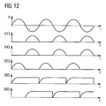
- the output of this operational amplifier OP13 is against reference potential GND to a voltage V13, the time course is shown in Figure 12 in comparison to the time course of the input current I1.
- This voltage V13 is zero during positive half waves of the input current I1 and assumes a positive value during negative half cycles of the input current I1, the signal value being proportional to that multiplied by -1 Signal value of the input current I1 during the negative half cycle.
- This input converter OP13, R13 thus fulfills the function of an inverting half-wave rectifier.
- the output signal of this input transducer is supplied to a current value output stage OP43, which comprises an operational amplifier whose plus input is supplied to the voltage V13, and at the output of which a momentary value signal V43 is available, which is zero during positive half cycles of the input current I1, and during negative halfwaves of this input current I1 has positive values that are proportional to the input current I1 multiplied by -1 during the negative halfwaves.
- a current value output stage OP43 which comprises an operational amplifier whose plus input is supplied to the voltage V13, and at the output of which a momentary value signal V43 is available, which is zero during positive half cycles of the input current I1, and during negative halfwaves of this input current I1 has positive values that are proportional to the input current I1 multiplied by -1 during the negative halfwaves.
- a second instantaneous value output stage OP53 which comprises an operational amplifier OP53, whose positive input is supplied to the input current I1 and whose negative input is coupled to the output thereof.
- a second instantaneous voltage V53 is available, which is zero during the negative half-cycle of the input current I1, and which is proportional to the input current I1 during the positive half-cycle.
- the diagnostic circuit 32 further includes first and second peaking rectifiers 34, 35, the first peaking rectifier 34 having its input current I1 directly supplied, and the second peaking rectifier being supplied with the output signal V13 of the input rectifier OP13, R13.
- the two peak value rectifiers 34, 35 each comprise an input amplifier OP63, OP73, to which the respective input signal I1 or V13 is fed at its plus input, and whose outputs are each followed by a diode D63, D73.
- the cathode connection of diode D63, D73 is fed back to the negative input of op-amp OP63, OP73.
- the operational amplifier OP63, OP73 with downstream diode D63, D73 causes peak rectification, whereby at the cathode terminal of the diode D63 of the first rectifier 34 in each case at the end of the positive half-wave, a value is applied, which is proportional to the maximum value of the measuring current I1 during the positive half-wave.
- a value is applied, which is proportional to the maximum value of the measuring current I1 during the positive half-wave.
- At the cathode terminal of the diode D73 of the second rectifier 35 is at the end of the negative half cycle to a positive voltage proportional to the amplitude of the measuring current I1 during the negative half cycle.
- the diodes D63, D73 in the two peak value rectifier units 34, 35 via a resistor R83, R93 each have a capacitor C83, C93 connected downstream, which serves as a holding member.
- a voltage across these capacitors C83, C93 is amplified by an output amplifier OP83, OP93 to provide a positive peak signal V83 and a negative peak signal V93.
- the positive peak signal V83 is proportional to the positive peak value of the input current I1 during the positive half cycle and the negative peak signal is proportional to the negative amplitude of the measurement current I1 during the negative half cycle.
- the positive peak signal V83, which is detected during the positive half cycle is held during the negative half cycle, referring to FIG. 12, while the negative peak signal V93, which is detected during the negative half cycle, is held during the positive half wave.
- Switches are connected in parallel with the capacitors C83, C93, and the switch S83, which is in parallel with the capacitor C83, is closed for a short time at the beginning of a positive half cycle to discharge the capacitor C83 before a next charging operation.
- a switch S93, which is in parallel with the capacitor C93, is closed at the beginning of a negative half-cycle for a short time, in order to charge the capacitor C93 before a next charging operation.
- Drive signals for these two switches S83, S93 can be derived, for example, by comparing the instantaneous value signals V43 and V53 by means of a comparator, not shown, to generate a square wave signal with a rising edge at the beginning of a negative half-wave and a falling edge at the beginning of a positive half-wave.
- This comparator signal may be supplied to a first delay element (not shown) which, after a rising edge of the comparator signal, closes the switch S93 for a predetermined period of time and, after a falling edge of the comparator signal, closes the switch S83 for a predetermined period of time.
- FIG. 11 Not shown in FIG. 11 are further evaluation units which further process the instantaneous value output signals V43, V53 or the peak value output signals V83, V93.
- This further processing can be done in a well-known manner. For example, to determine whether the positive amplitude of the input current I1 is significantly different from the negative amplitude of the sense current I1, the difference of the peak output signals V83, V93 could easily be determined to provide an error signal if this difference exceeds a predetermined value generate and prevent further control of the lamp.
- the diagnostic circuit also includes a lamp detector comprising a switch S33 connected between the input IN and the reference potential GND.
- This switch S33 is in a manner not shown, for example, to a lamp socket, in which the lamp 10 is inserted, attached and closed when no lamp is inserted into the socket.
- the measuring input IN is at reference potential GND, which is detected by a comparator OP33, which compares the potential at the measuring input with another reference potential REF33, to drive the half-bridge circuit Q1, Q2 or the (non-existent) lamp prevent.
- Figures 13 and 14 show another embodiment of a drive circuit or a lamp ballast for a fluorescent lamp.
- the resistance element R1 is part of a DC current path to which a detector circuit 40 for detecting a current flowing through the DC current path is coupled.
- the DC path in the embodiment of the terminal K1 for the half-bridge circuit Q1., Q2, at which a supply potential for the half-bridge circuit is applied, via a further resistance element R2, the resonance inductor L1, the first lamp filament or lamp electrode 11 and the resistance element R1 to one Terminal for a reference potential Vcc, this reference potential Vcc being, for example, a supply potential of the components of the detector circuit 40 and the control circuit 21 driving the half-bridge circuit Q1, Q2.
- This DC path which runs over the first lamp filament 11 of the fluorescent lamp 10 is only with inserted fluorescent lamp 10 and intact, i. electrically conductive, first lamp filament 11 closed.
- the detector circuit 40 has a current detector 44 which is connected in the DC path and which is connected to an evaluation circuit 45, which generates a first detector signal S45 which is supplied to the control circuit 21.
- a first diode D41 is connected, which allows a current only in the drawn in Figure 13 for the current I1 direction.
- a second diode D42 is present, which is connected between the reference potential GND and the node common to the resistance element R1 and the first diode D41.
- the DC path in conjunction with the detector circuit 40 serves to detect if a fluorescent lamp 10 is present and if the lamp is intact.
- a control of the half-bridge circuit Q1, Q2 by the control circuit 21 is omitted in this drive circuit, when the control circuit via the first detector signal S45 receives the information that the DC current flowing across the DC path is below a predetermined threshold, indicating an unused or non-intact fluorescent lamp 10 indicates.
- the comparison threshold for the detected current is generated in the example by a threshold detector 45 to which the current detector 44 is coupled.
- the resistance elements R1, R2 of the DC current path are selected, for example, such that the DC current flowing through the DC current path when the fluorescent lamp 10 is inserted and intact is approximately between 20 ⁇ A and 200 ⁇ A.
- the detector circuit 40 can be used in particular in connection with the already explained diagnostic circuit 30, as shown in FIG.
- a switch S13 is connected between the resistance element R1 and the remaining components, ie the current-voltage converter 31 and the evaluation circuit 32 of the diagnostic circuit 30, which is also shown in FIG.
- This switch S13 is also controlled by the control circuit 21.
- the control circuit 21 for the half-bridge circuit Q1, Q2, the diagnosis circuit 30 and the detector circuit 40 preferably form a common integrated control circuit for the lamp ballast, which are integrated in a common semiconductor chip.
- the control circuit 21 After interruption of the control of the half-bridge due to wear, the control circuit 21 detects via the first detector signal S45 whether the current flowing through the DC current path is present after a delay time of zero a positive value increases. The rise of this direct current from zero to a positive, above a predetermined threshold value after a delay time after a wear-related shutdown of the half-bridge indicates a change of the fluorescent lamp by a user, the control circuit after detection of such a lamp change the half-bridge Q1, Q2 again.
- the switch S13 can be dispensed with in the embodiment shown in FIG. 14, in which the detector circuit 40 is used without the components 31, 32 of the diagnostic circuit 30 which detect wear.
- a reference voltage source REF41, a resistor R41 connected in series with the reference voltage source REF41 and a further diode D43 are provided in the detector circuit 40, the series circuit with the reference voltage source REF41, the switch SW41, the resistor R41 and the diode D43 between reference potential GND and the resistance element R1 are connected.
- a second threshold detector 46, which supplies a second detector signal S46 to the control circuit 21, is connected to the node common to the resistor R41 and to the diode D43.
- the switch SW41 is also controlled in a manner not shown by the control circuit 21 and before the start of the half-bridge Q1, Q2, when the switch S13 is open, closed.
- the node common to the diode D43 and the resistor R1 is then at a potential which corresponds at least to the reference potential REF41.
- This node which is common to the diode D43 and the resistor R1, constitutes an interface between the integrated control circuit with the components 21, 30, 40 to the "outside world." If this node is connected to a reference potential GND by the manufacturer of the ballast, this is only possible, however if the manufacturer uses the resistive elements R1, R2 is not equipped in the circuit, the control circuit 21 can be informed in this way that the resistance elements R1, R2 are not equipped and that the diagnosis circuit is not to be used in total. This information is communicated to the control circuit 21 via the second detector signal S46 from the second threshold detector 46, which evaluates the potential at the node common to the resistor R41 and the diode D43.
- the described option is useful in integrated control circuits, which can be optionally used for one or more lamps and have a corresponding number of diagnostic circuits to shut down the diagnostic circuits not required.
Landscapes
- Circuit Arrangements For Discharge Lamps (AREA)
- Inverter Devices (AREA)
- Dc-Dc Converters (AREA)
Applications Claiming Priority (1)
| Application Number | Priority Date | Filing Date | Title |
|---|---|---|---|
| DE102004037390A DE102004037390B4 (de) | 2004-08-02 | 2004-08-02 | Ansteuerschaltung für eine Leuchtstofflampe mit einer Diagnoseschaltung und Verfahren zur Diagnose einer Leuchtstofflampe |
Publications (2)
| Publication Number | Publication Date |
|---|---|
| EP1624731A2 true EP1624731A2 (fr) | 2006-02-08 |
| EP1624731A3 EP1624731A3 (fr) | 2007-12-26 |
Family
ID=35134561
Family Applications (1)
| Application Number | Title | Priority Date | Filing Date |
|---|---|---|---|
| EP05013377A Withdrawn EP1624731A3 (fr) | 2004-08-02 | 2005-06-21 | Circuit avec fonction de surveillance pour lampe fluorescente, et méthode de surveillance d' une lampe fluorescente |
Country Status (4)
| Country | Link |
|---|---|
| US (1) | US7378807B2 (fr) |
| EP (1) | EP1624731A3 (fr) |
| CN (2) | CN1747618B (fr) |
| DE (1) | DE102004037390B4 (fr) |
Cited By (1)
| Publication number | Priority date | Publication date | Assignee | Title |
|---|---|---|---|---|
| ITVA20130002A1 (it) * | 2013-01-11 | 2014-07-12 | Tci Telecomunicazioni Italia Srl | Ballast con protezione elettronica |
Families Citing this family (14)
| Publication number | Priority date | Publication date | Assignee | Title |
|---|---|---|---|---|
| US7592753B2 (en) * | 1999-06-21 | 2009-09-22 | Access Business Group International Llc | Inductively-powered gas discharge lamp circuit |
| KR101176086B1 (ko) * | 2006-05-30 | 2012-08-22 | 페어차일드코리아반도체 주식회사 | 형광램프의 수명말기 검출회로 |
| US7821208B2 (en) * | 2007-01-08 | 2010-10-26 | Access Business Group International Llc | Inductively-powered gas discharge lamp circuit |
| WO2008128565A1 (fr) * | 2007-04-19 | 2008-10-30 | Osram Gesellschaft mit beschränkter Haftung | Circuit d'excitation pour lampe fluorescente, procédé de fonctionnement dudit circuit et système comprenant ledit circuit |
| KR101394613B1 (ko) * | 2007-07-04 | 2014-05-14 | 페어차일드코리아반도체 주식회사 | 진단 장치 및 이를 이용하는 램프 안정기 회로 |
| US7834552B2 (en) | 2007-07-17 | 2010-11-16 | Infineon Technologies Austria Ag | Controlling a lamp ballast |
| TWI370706B (en) * | 2008-01-22 | 2012-08-11 | Coretronic Corp | Waveform management systems and methods for ballasts |
| KR101478352B1 (ko) * | 2008-11-28 | 2015-01-06 | 페어차일드코리아반도체 주식회사 | 비정상 스위칭 감시 장치 및 감시 방법 |
| JP2010257659A (ja) * | 2009-04-22 | 2010-11-11 | Panasonic Electric Works Co Ltd | 高圧放電灯点灯装置及びそれを用いた照明器具 |
| US8963442B2 (en) * | 2009-11-04 | 2015-02-24 | International Rectifier Corporation | Driver circuit with an increased power factor |
| KR101145637B1 (ko) * | 2010-06-23 | 2012-05-23 | 현대자동차주식회사 | 전압변환기의 진단장치 및 방법 |
| US8487664B2 (en) * | 2010-11-30 | 2013-07-16 | Infineon Technologies Ag | System and method for driving a switch |
| TW201501572A (zh) * | 2013-06-17 | 2015-01-01 | Skynet Electronic Co Ltd | 燈絲短路型之節能燈 |
| EP3089347B1 (fr) * | 2015-04-27 | 2018-06-27 | ABB Schweiz AG | Procédé permettant d'acquérir des valeurs indicatives d'un courant alternatif d'un onduleur et onduleur et circuit associés |
Family Cites Families (14)
| Publication number | Priority date | Publication date | Assignee | Title |
|---|---|---|---|---|
| CN2144390Y (zh) * | 1992-12-23 | 1993-10-20 | 邓诗燮 | 互锁输出式节能荧光灯电子镇流器 |
| US5475284A (en) * | 1994-05-03 | 1995-12-12 | Osram Sylvania Inc. | Ballast containing circuit for measuring increase in DC voltage component |
| US5808422A (en) * | 1996-05-10 | 1998-09-15 | Philips Electronics North America | Lamp ballast with lamp rectification detection circuitry |
| US6008593A (en) * | 1997-02-12 | 1999-12-28 | International Rectifier Corporation | Closed-loop/dimming ballast controller integrated circuits |
| DE19715341C1 (de) * | 1997-04-12 | 1998-10-15 | Vossloh Schwabe Gmbh | Elektronisches Vorschaltgerät mit automatischem Wiederanlauf |
| US5925990A (en) * | 1997-12-19 | 1999-07-20 | Energy Savings, Inc. | Microprocessor controlled electronic ballast |
| ATE213901T1 (de) * | 1997-12-23 | 2002-03-15 | Tridonic Bauelemente | Verfahren und vorrichtung zum erfassen des in einer gasentladungslampe auftretenden gleichrichteffekts |
| US5973943A (en) * | 1998-01-05 | 1999-10-26 | International Rectifier Corporation | Non zero-voltage switching protection circuit |
| US6008592A (en) * | 1998-06-10 | 1999-12-28 | International Rectifier Corporation | End of lamp life or false lamp detection circuit for an electronic ballast |
| JP2001015289A (ja) * | 1999-04-28 | 2001-01-19 | Mitsubishi Electric Corp | 放電灯点灯装置 |
| US6366032B1 (en) * | 2000-01-28 | 2002-04-02 | Robertson Worldwide, Inc. | Fluorescent lamp ballast with integrated circuit |
| KR100539721B1 (ko) * | 2000-10-20 | 2005-12-29 | 인터내쇼널 렉티파이어 코포레이션 | 역률 보정 기능을 갖는 안정기 제어 집적 회로 |
| DE10206731B4 (de) | 2002-02-18 | 2016-12-22 | Tridonic Gmbh & Co Kg | Lampensensor für ein Vorschaltgerät zum Betrieb einer Gasentladunslampe |
| US6853153B2 (en) * | 2002-02-26 | 2005-02-08 | Analog Microelectronics, Inc. | System and method for powering cold cathode fluorescent lighting |
-
2004
- 2004-08-02 DE DE102004037390A patent/DE102004037390B4/de not_active Expired - Fee Related
-
2005
- 2005-06-21 EP EP05013377A patent/EP1624731A3/fr not_active Withdrawn
- 2005-08-02 CN CN200510088264.8A patent/CN1747618B/zh not_active Expired - Fee Related
- 2005-08-02 CN CN201210032646.9A patent/CN102612241B/zh not_active Expired - Fee Related
- 2005-08-02 US US11/195,376 patent/US7378807B2/en not_active Expired - Lifetime
Cited By (1)
| Publication number | Priority date | Publication date | Assignee | Title |
|---|---|---|---|---|
| ITVA20130002A1 (it) * | 2013-01-11 | 2014-07-12 | Tci Telecomunicazioni Italia Srl | Ballast con protezione elettronica |
Also Published As
| Publication number | Publication date |
|---|---|
| CN1747618B (zh) | 2012-04-25 |
| US7378807B2 (en) | 2008-05-27 |
| CN102612241B (zh) | 2015-08-19 |
| US20060033450A1 (en) | 2006-02-16 |
| CN1747618A (zh) | 2006-03-15 |
| EP1624731A3 (fr) | 2007-12-26 |
| DE102004037390A1 (de) | 2006-03-16 |
| CN102612241A (zh) | 2012-07-25 |
| DE102004037390B4 (de) | 2008-10-23 |
Similar Documents
| Publication | Publication Date | Title |
|---|---|---|
| DE102004037390B4 (de) | Ansteuerschaltung für eine Leuchtstofflampe mit einer Diagnoseschaltung und Verfahren zur Diagnose einer Leuchtstofflampe | |
| EP1519638B1 (fr) | Méthode pour commander une lampe à décharge basse pression | |
| DE102010030134B4 (de) | Ermittlung der Totzeit bei der Ansteuerung einer Halbbrücke | |
| DE102004037388B4 (de) | Verfahren zur Detektion eines Nicht-Nullspannungsschaltbetriebs eines Vorschaltgeräts für Leuchtstofflampen und Vorschaltgerät | |
| DE102007040383A1 (de) | Entladungslampen-Zündschaltung | |
| DE19622803A1 (de) | Lichtstromkreis für Entladungslampe | |
| DE102009023505A1 (de) | Schaltungsanordnung für einen Piezotransformator und dazugehörendes Verfahren | |
| DE10328718A1 (de) | Verfahren zum Betrieb mindestens einer Niederdruckentladungslampe und Betriebsgerät für mindestens eine Niederdruckentladungslampe | |
| US20080265900A1 (en) | Method and Apparatus for Monitoring the Operation of a Gas Discharge Lamp | |
| EP1424881B1 (fr) | Dispositif et méthode pour commander une lampe fluorescente | |
| DE10240110A1 (de) | Entladungslampen-Beleuchtungsschaltung | |
| EP2274960B1 (fr) | Procédé et agencement de circuits pour faire fonctionner au moins une lampe à décharge | |
| EP1040733B1 (fr) | Ballast electronique | |
| EP1945008B1 (fr) | Capteur de lampes pour un appareil de montage destiné au fonctionnement d'une lampe à décharge | |
| EP1651014A1 (fr) | Méthode et circuit utilisant la mesure du courant actif pour alimenter une lampe | |
| DE102004037389C5 (de) | Verfahren zur Ansteuerung einer eine Leuchtstofflampe aufweisenden Last zur Optimierung des Zündvorganges | |
| EP1920644B1 (fr) | Ballast electronique pour lampes a decharge comprenant un circuit de controle de fin de vie | |
| DE102004009994A1 (de) | Überstrom- und Mittenpunktspannungserfassung | |
| DE102006019085A1 (de) | Entladungslampen-Lichtstromkreis | |
| EP2127499B1 (fr) | Montage de commande d'au moins une lampe fluorescente | |
| EP2796012A1 (fr) | Procédé, appareillage d'alimentation et système d'éclairage, avec détection d'effet de redressement de lampes | |
| DE102004039414B4 (de) | Entladungslampenansteuerschaltung | |
| EP1040732B1 (fr) | Procede de detection de changement de lampe et ballast electronique destine au fonctionnement de lampes a decharge a l'aide d'un tel procede de detection de changement de lampe | |
| WO1999034648A1 (de) | Elektronisches vorschaltgerät | |
| DE102010029511B4 (de) | Schaltungsanordnung zum Betreiben einer Entladungslampe |
Legal Events
| Date | Code | Title | Description |
|---|---|---|---|
| PUAI | Public reference made under article 153(3) epc to a published international application that has entered the european phase |
Free format text: ORIGINAL CODE: 0009012 |
|
| AK | Designated contracting states |
Kind code of ref document: A2 Designated state(s): AT BE BG CH CY CZ DE DK EE ES FI FR GB GR HU IE IS IT LI LT LU MC NL PL PT RO SE SI SK TR |
|
| AX | Request for extension of the european patent |
Extension state: AL BA HR LV MK YU |
|
| PUAL | Search report despatched |
Free format text: ORIGINAL CODE: 0009013 |
|
| AK | Designated contracting states |
Kind code of ref document: A3 Designated state(s): AT BE BG CH CY CZ DE DK EE ES FI FR GB GR HU IE IS IT LI LT LU MC NL PL PT RO SE SI SK TR |
|
| AX | Request for extension of the european patent |
Extension state: AL BA HR LV MK YU |
|
| 17P | Request for examination filed |
Effective date: 20080220 |
|
| AKX | Designation fees paid |
Designated state(s): AT DE FR IT NL SE |
|
| 17Q | First examination report despatched |
Effective date: 20081202 |
|
| STAA | Information on the status of an ep patent application or granted ep patent |
Free format text: STATUS: THE APPLICATION IS DEEMED TO BE WITHDRAWN |
|
| 18D | Application deemed to be withdrawn |
Effective date: 20090613 |