EP1626437B1 - Verfahren zur Herstellung von gestapelten Inselstrukturen aus einem Halbleitermaterial in einem anderen Halbleitermaterial - Google Patents
Verfahren zur Herstellung von gestapelten Inselstrukturen aus einem Halbleitermaterial in einem anderen Halbleitermaterial Download PDFInfo
- Publication number
- EP1626437B1 EP1626437B1 EP05107422A EP05107422A EP1626437B1 EP 1626437 B1 EP1626437 B1 EP 1626437B1 EP 05107422 A EP05107422 A EP 05107422A EP 05107422 A EP05107422 A EP 05107422A EP 1626437 B1 EP1626437 B1 EP 1626437B1
- Authority
- EP
- European Patent Office
- Prior art keywords
- islands
- semiconducting material
- germanium
- partial pressure
- semiconductor material
- Prior art date
- Legal status (The legal status is an assumption and is not a legal conclusion. Google has not performed a legal analysis and makes no representation as to the accuracy of the status listed.)
- Expired - Lifetime
Links
Images
Classifications
-
- H—ELECTRICITY
- H10—SEMICONDUCTOR DEVICES; ELECTRIC SOLID-STATE DEVICES NOT OTHERWISE PROVIDED FOR
- H10P—GENERIC PROCESSES OR APPARATUS FOR THE MANUFACTURE OR TREATMENT OF DEVICES COVERED BY CLASS H10
- H10P14/00—Formation of materials, e.g. in the shape of layers or pillars
- H10P14/20—Formation of materials, e.g. in the shape of layers or pillars of semiconductor materials
- H10P14/29—Formation of materials, e.g. in the shape of layers or pillars of semiconductor materials characterised by the substrates
- H10P14/2901—Materials
- H10P14/2902—Materials being Group IVA materials
- H10P14/2905—Silicon, silicon germanium or germanium
-
- B—PERFORMING OPERATIONS; TRANSPORTING
- B82—NANOTECHNOLOGY
- B82Y—SPECIFIC USES OR APPLICATIONS OF NANOSTRUCTURES; MEASUREMENT OR ANALYSIS OF NANOSTRUCTURES; MANUFACTURE OR TREATMENT OF NANOSTRUCTURES
- B82Y10/00—Nanotechnology for information processing, storage or transmission, e.g. quantum computing or single electron logic
-
- H—ELECTRICITY
- H10—SEMICONDUCTOR DEVICES; ELECTRIC SOLID-STATE DEVICES NOT OTHERWISE PROVIDED FOR
- H10D—INORGANIC ELECTRIC SEMICONDUCTOR DEVICES
- H10D62/00—Semiconductor bodies, or regions thereof, of devices having potential barriers
- H10D62/80—Semiconductor bodies, or regions thereof, of devices having potential barriers characterised by the materials
- H10D62/81—Semiconductor bodies, or regions thereof, of devices having potential barriers characterised by the materials of structures exhibiting quantum-confinement effects, e.g. single quantum wells; of structures having periodic or quasi-periodic potential variation
- H10D62/812—Single quantum well structures
- H10D62/814—Quantum box structures
-
- H—ELECTRICITY
- H10—SEMICONDUCTOR DEVICES; ELECTRIC SOLID-STATE DEVICES NOT OTHERWISE PROVIDED FOR
- H10P—GENERIC PROCESSES OR APPARATUS FOR THE MANUFACTURE OR TREATMENT OF DEVICES COVERED BY CLASS H10
- H10P14/00—Formation of materials, e.g. in the shape of layers or pillars
- H10P14/20—Formation of materials, e.g. in the shape of layers or pillars of semiconductor materials
- H10P14/24—Formation of materials, e.g. in the shape of layers or pillars of semiconductor materials using chemical vapour deposition [CVD]
-
- H—ELECTRICITY
- H10—SEMICONDUCTOR DEVICES; ELECTRIC SOLID-STATE DEVICES NOT OTHERWISE PROVIDED FOR
- H10P—GENERIC PROCESSES OR APPARATUS FOR THE MANUFACTURE OR TREATMENT OF DEVICES COVERED BY CLASS H10
- H10P14/00—Formation of materials, e.g. in the shape of layers or pillars
- H10P14/20—Formation of materials, e.g. in the shape of layers or pillars of semiconductor materials
- H10P14/32—Formation of materials, e.g. in the shape of layers or pillars of semiconductor materials characterised by intermediate layers between substrates and deposited layers
- H10P14/3202—Materials thereof
- H10P14/3204—Materials thereof being Group IVA semiconducting materials
- H10P14/3211—Silicon, silicon germanium or germanium
-
- H—ELECTRICITY
- H10—SEMICONDUCTOR DEVICES; ELECTRIC SOLID-STATE DEVICES NOT OTHERWISE PROVIDED FOR
- H10P—GENERIC PROCESSES OR APPARATUS FOR THE MANUFACTURE OR TREATMENT OF DEVICES COVERED BY CLASS H10
- H10P14/00—Formation of materials, e.g. in the shape of layers or pillars
- H10P14/20—Formation of materials, e.g. in the shape of layers or pillars of semiconductor materials
- H10P14/32—Formation of materials, e.g. in the shape of layers or pillars of semiconductor materials characterised by intermediate layers between substrates and deposited layers
- H10P14/3242—Structure
- H10P14/3256—Microstructure
-
- H—ELECTRICITY
- H10—SEMICONDUCTOR DEVICES; ELECTRIC SOLID-STATE DEVICES NOT OTHERWISE PROVIDED FOR
- H10P—GENERIC PROCESSES OR APPARATUS FOR THE MANUFACTURE OR TREATMENT OF DEVICES COVERED BY CLASS H10
- H10P14/00—Formation of materials, e.g. in the shape of layers or pillars
- H10P14/20—Formation of materials, e.g. in the shape of layers or pillars of semiconductor materials
- H10P14/34—Deposited materials, e.g. layers
- H10P14/3402—Deposited materials, e.g. layers characterised by the chemical composition
- H10P14/3404—Deposited materials, e.g. layers characterised by the chemical composition being Group IVA materials
- H10P14/3411—Silicon, silicon germanium or germanium
-
- H—ELECTRICITY
- H10—SEMICONDUCTOR DEVICES; ELECTRIC SOLID-STATE DEVICES NOT OTHERWISE PROVIDED FOR
- H10P—GENERIC PROCESSES OR APPARATUS FOR THE MANUFACTURE OR TREATMENT OF DEVICES COVERED BY CLASS H10
- H10P14/00—Formation of materials, e.g. in the shape of layers or pillars
- H10P14/20—Formation of materials, e.g. in the shape of layers or pillars of semiconductor materials
- H10P14/34—Deposited materials, e.g. layers
- H10P14/3451—Structure
- H10P14/3452—Microstructure
Definitions
- the invention relates to a method for producing stacks of islands of semiconductor material encapsulated in another semiconductor material. It relates in particular to the realization of stacks of germanium islands encapsulated in silicon.
- Integrated circuits made with silicon-based microelectronics technology are becoming more complex and fast.
- the devices and functional groups of these integrated circuits are now connected by metal lines.
- the latter have limitations, in particular an RC time constant and a high heat dissipation which, in spite of the technological evolutions, will not be able to make it possible to continue increasing the operating frequencies of the microprocessors.
- the idea of using optical links as an alternative to metallic interconnects is emerging. Compared to metallic lines, the optical links offer: a gain in speed, a reduction of the signal alteration, a propagation without heat dissipation and the possibility of wavelength multiplexing.
- Optical (fiber) links are already used in networks on a larger or smaller scale (networks local to international networks), the concept of "all-optical" connections from transistors to networks is emerging.
- germanium is deposited by epitaxy either in the form of "thick" layers (several hundred nanometers), or in the form of an alloy with silicon to produce multi-quantum wells (stacking layers silicon and silicon-germanium alloy). These two types of structures constitute the absorption zone of the incident photons in the photo-detectors.
- the properties optical thick layers of pure germanium are degraded by the presence of dislocations (due to the disagreement mesh with the silicon substrate) and difficulties of integration in the devices are encountered (high layer roughness, problematic contact ... ).
- the multi-quantum wells of silicon layers and silicon-germanium alloys they have an absorption coefficient which is too low for effective photo-detection.
- the growth of germanium on silicon according to the Stranski-Krastanov mode is an alternative to the two methods described above.
- An example of photodetector formation consisting of germanium islands is given by El Kurdi et al. in Physica E 16, 523 (2003).
- the Stranski-Krastanov growth mode makes it possible to form islands of germanium of small size, with a relatively homogeneous distribution of this size.
- Two types of islets are usually formed: small pyramids and domes. The prolongation of the deposit leads to the formation of large domes that are plastically relaxed, that is, these domes contain dislocations.
- the small domes, in which the stresses are released elastically, are the desired structures.
- Stacks of germanium island layers can be made by separating the island layers by silicon layers, analogously to the multi-quantum wells. These stacks make it possible to absorb incident photons more efficiently than the multi-quantum wells based on silicon-germanium alloy layers, while posing less integration difficulties than pure germanium.
- the optical properties of the germanium island layers are sensitive to the characteristics of the islets, mainly their size, size distribution, surface density, and composition.
- 6,596,555 have proposed a sequence for the formation of a simple island plan, based on the generation of a larger number of islet formation sites due to a high germane flow at the beginning of deposition. They propose to form stacks by covering this layer of islets with silicon and repeating this sequence as many times as necessary. However, this process requires very short injection times.
- the present invention provides an alternative to US Patent 6,596,555 using deposition parameters that are more easily controllable and reproducible.
- This plan will be called “sacrificial plan” because it can be achieved under growing conditions (pressure and / or temperature) that do not necessarily make it possible to obtain good optical properties.
- the sacrificial plane will make it possible to generate numerous nucleation sites for the following island plans. These subsequent island plans will be realized under growth conditions leading to good optical properties.
- the subject of the invention is therefore a method for producing a stacked structure of island planes of a first semiconductor material encapsulated in a second semiconductor material, on a substrate, comprising alternately depositing island planes of first material. semiconductor and encapsulating layers of second semiconductor material, the island planes of first semiconductor material being made at an optimal growth temperature and under an optimum precursor gas partial pressure to obtain a stacked structure whose optical properties allow a use as optical interconnections within integrated circuits, the method being characterized in that the stacked structure is formed on a plane of islands of third semiconductor material, called the sacrificial plane, encapsulated in a fourth semiconductor material, the islands of the plane sacrificial being carried out under growth conditions making it possible to obtain high densities of small islands, ie at a temperature below the optimum growth temperature and / or under a higher precursor gas partial pressure. at the optimum partial pressure.
- the first semiconductor material and the third semiconductor material may be identical.
- the second semiconductor material and the fourth semiconductor material may also be identical.
- the first semiconductor material is germanium and the second semiconductor material is silicon.
- the islands of germanium can be deposited at a temperature of the order of 650 ° C and a partial pressure of germane of the order of 0.11 Pa (0.83 mTorr).
- the third semiconductor material is germanium and the fourth semiconductor material is silicon.
- the germanium islands of the sacrificial plane can be deposited at a temperature of the order of 650 ° C and at a germane partial pressure of the order of 0.88 Pa (6.56 mTorr). They can also be deposited at a temperature of the order of 550 ° C. and under a germane partial pressure of the order of 0.11 Pa (0.83 mTorr).
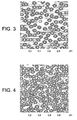
- the figure 2 is a diagram representing the density of these islands of germanium as a function of the partial pressure of germane. On the diagram of the figure 2 curve 1 refers to the pyramids obtained and curve 2 refers to the domes obtained.
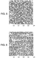
- the figure 3 reproduces an AFM (obtained by an atomic force microscope) image of a surface of germanium islands made on one side of a silicon substrate at the optimum growth temperature (650 ° C) and with a partial pressure of germane standard of 0.11 Pa (0.83 mTorr).
- the density of islands obtained is less than 10 10 / cm 2 .
- the figure 4 reproduces an AFM image of a surface of germanium islands made on one side of a silicon substrate at the optimal growth temperature (650 ° C) and with a high germane partial pressure (0.88 Pa (6.56 mTorr )). It is easy to see, by comparing these two pictures, that the density of the islets shown on the photograph of the figure 4 is higher (some 10 10 / cm 2 ) than the density of the islets shown on the photograph of the figure 3 . We also note that the size of the islets shown on the photograph of the figure 4 is smaller than the size of the islets shown on the snapshot of the figure 3 .
- a stack of silicon-encapsulated islands of germanium islands was made by a first variant of the process according to the invention.
- a stack of silicon-encapsulated islands of germanium islands has also been made on one side of a silicon substrate by a second variant of the process according to the invention.
- a sacrificial plane is first produced at a temperature of 650 ° C. and at a partial pressure of germane of 0.88 Pa (6.56 mTorr).
- the following shots are made at 650 ° C (optimum growth temperature) and at a germane partial pressure of 0.11 Pa (0.83 mTorr) (standard pressure).
- a sacrificial plane is first produced at a temperature of 550 ° C. and at a partial germane pressure of 0.11 Pa (0.83 mTorr) (standard pressure).
- the following shots are made at 650 ° C (optimum growth temperature) and at a germane partial pressure of 0.11 Pa (0.83 mTorr) (standard pressure).
- the figure 5 reproduces an AFM image of the surface of a stack of two planes of germanium islands encapsulated in silicon and made on one side of a silicon substrate, according to a method of the prior art.
- the deposition temperature for these two planes is 650 ° C. and the partial pressure of germane for these two planes is 0.11 Pa (0.83 mTorr).
- the square-shaped structures observed on the AFM snapshot are formed during the encapsulation of the foreground islets.
- the surface density of islands for the second plane is less than 5.10 9 cm -2 . It is reduced by a factor of two compared to the foreground.
- the figure 6 reproduces an AFM image of the surface of a stack of two planes of germanium islands encapsulated in silicon and made on one side of a silicon substrate, according to the method of the present invention.
- the deposition temperature of the sacrificial plane is 650 ° C. and the partial pressure of germane is 0.88 Pa (6.56 mTorr).
- the deposition temperature of the following plane is 650 ° C. and the partial pressure of germane is 0.11 Pa (0.83 mTorr).
- the surface density of islands for the second plane is then twice as high as for the second plane of the previous example (according to the known art) and the islets are also smaller.
- the invention is also applicable to any heteroepitaxy process for making island stacks of semiconductor materials (IV-IV, III-V, etc.).
Landscapes
- Engineering & Computer Science (AREA)
- Chemical & Material Sciences (AREA)
- Nanotechnology (AREA)
- Physics & Mathematics (AREA)
- Mathematical Physics (AREA)
- Theoretical Computer Science (AREA)
- Crystallography & Structural Chemistry (AREA)
- Recrystallisation Techniques (AREA)
- Pharmaceuticals Containing Other Organic And Inorganic Compounds (AREA)
- Crystals, And After-Treatments Of Crystals (AREA)
- Element Separation (AREA)
Claims (8)
- Verfahren zur Herstellung einer Schichtstapel-Struktur von Ebenen von Inseln aus einem ersten Halbleitermaterial, die in einem zweiten Halbleitermaterial gekapselt sind, auf einem Substrat, das Verfahren umfassend das alternierende Abscheiden von Ebenen von Inseln aus erstem Halbleitermaterial und von Kapselungsschichten aus zweitem Halbleitermaterial, wobei die Ebenen von Inseln aus erstem Halbleitermaterial bei einer Temperatur optimalen Wachstums und bei einem optimalen Partialdruck eines Vorläufergases erzeugt werden zur Erzielungs einer Stapelstruktur, deren optische Eigenschaften die Schaffung von opto-elektronischen Bauteilen zur Verbindung integrierter Schaltungen gestatten, das Verfahren dadurch gekennzeichnet, dass die Stapelstruktur auf einer Ebene von Inseln aus einem dritten Halbleitermaterial erzeugt wird, die als opferbare oder verlorene Ebene bezeichnet wird und in einem vierten Halbleitermaterial gekapselt ist, wobei die Inseln der opferbaren Ebene unter Wachstumsbedingungen erzeugt werden, welche die Erzielung hoher Dichten von Inseln kleiner Abmessungen gestatten, das heißt bei einer Temperatur, die niedriger als die optimale Wachstumstemperatur ist und /oder unter einem Partialdruck des Vorläufergases, der über dem optimalen Partialdruck liegt.
- Verfahrren nach Anspruch 1, dadurch gekennzeichnet, dass das erste Halbleitermaterial und das dritte Halbleitermaterial gleich sind.
- Verfahren nach einem der Ansprüche 1 oder 2, dadurch gekennzeichnet, dass das zweite Halbleitermaterial und das vierte Halbleitermaterial gleich sind.
- Verfahren nach einem der Ansprüche 1 bis 3, dadurch gekennzeichnet, dass das erste Halbleitermaterial Germanium und das zweite Halbleitermaterial Silizium ist.
- Verfahren nach Anspruch 4, dadurch gekennzeichnet, dass die Inseln aus Germanium bei einer Temperatur in der Größenordnung von 650 ° C und unter einem Partialdruck von German der Größenordnung von 0,11 Pa (0,83 mTorr) abgeschieden werden.
- Verfahren nach einem der Ansprüche 1 bis 5, dadurch gekennzeichnet, dass das dritte Halbleitermaterial Germanium und das vierte Halbleitermaterial Silizium ist.
- Verfahren nach Anspruch 6, dadurch gekennzeichnet, daß die Germanium-Inseln der opferbaren oder verlorenen Ebene bei einer Temperatur in der Größenordnung von 650 °C und bei einem Partialdruck des German in der Größenordnung von 0,88 Pa (6,56 mTorr) abgeschieden werden.
- Verfahren nach Anspruch 6 , dadurch gekennzeichnet, daß die Germanium-Inseln der opferbaren bzw. verlorenen Ebene bei einer Temperatur in der Größenordnung von 550 ° C und bei einem Partialdruck des German in der Größenordnung von 0,11 Pa (0,83 mTorr) abgeschieden werden.
Applications Claiming Priority (1)
| Application Number | Priority Date | Filing Date | Title |
|---|---|---|---|
| FR0451850A FR2874285B1 (fr) | 2004-08-13 | 2004-08-13 | Procede de realisation d'empilements d'ilots de materiau semi-conducteur encapsules dans un autre materiau semi-conducteur |
Publications (2)
| Publication Number | Publication Date |
|---|---|
| EP1626437A1 EP1626437A1 (de) | 2006-02-15 |
| EP1626437B1 true EP1626437B1 (de) | 2010-07-07 |
Family
ID=34948643
Family Applications (1)
| Application Number | Title | Priority Date | Filing Date |
|---|---|---|---|
| EP05107422A Expired - Lifetime EP1626437B1 (de) | 2004-08-13 | 2005-08-12 | Verfahren zur Herstellung von gestapelten Inselstrukturen aus einem Halbleitermaterial in einem anderen Halbleitermaterial |
Country Status (5)
| Country | Link |
|---|---|
| US (1) | US7494831B2 (de) |
| EP (1) | EP1626437B1 (de) |
| AT (1) | ATE473514T1 (de) |
| DE (1) | DE602005022143D1 (de) |
| FR (1) | FR2874285B1 (de) |
Family Cites Families (7)
| Publication number | Priority date | Publication date | Assignee | Title |
|---|---|---|---|---|
| US5265957A (en) * | 1992-08-11 | 1993-11-30 | Texas Instruments Incorporated | Wireless temperature calibration device and method |
| US5293050A (en) * | 1993-03-25 | 1994-03-08 | International Business Machines Corporation | Semiconductor quantum dot light emitting/detecting devices |
| US5888885A (en) * | 1997-05-14 | 1999-03-30 | Lucent Technologies Inc. | Method for fabricating three-dimensional quantum dot arrays and resulting products |
| FR2812763B1 (fr) * | 2000-08-04 | 2002-10-31 | St Microelectronics Sa | Formation de boites quantiques |
| DE60220803T2 (de) * | 2002-11-29 | 2008-03-06 | MAX-PLANCK-Gesellschaft zur Förderung der Wissenschaften e.V. | Halbleiterstruktur für Infrarotbereich und Herstellungsverfahren |
| WO2005015579A2 (en) * | 2002-12-02 | 2005-02-17 | North Carolina State University | Methods of forming three-dimensional nanodot arrays in a matrix |
| US20050181624A1 (en) * | 2004-02-13 | 2005-08-18 | International Business Machines Corporation | Method of forming quantum dots at predetermined positions on a substrate |
-
2004
- 2004-08-13 FR FR0451850A patent/FR2874285B1/fr not_active Expired - Fee Related
-
2005
- 2005-08-12 DE DE602005022143T patent/DE602005022143D1/de not_active Expired - Lifetime
- 2005-08-12 EP EP05107422A patent/EP1626437B1/de not_active Expired - Lifetime
- 2005-08-12 US US11/202,316 patent/US7494831B2/en active Active
- 2005-08-12 AT AT05107422T patent/ATE473514T1/de not_active IP Right Cessation
Also Published As
| Publication number | Publication date |
|---|---|
| ATE473514T1 (de) | 2010-07-15 |
| DE602005022143D1 (de) | 2010-08-19 |
| US20060035399A1 (en) | 2006-02-16 |
| FR2874285B1 (fr) | 2006-10-13 |
| FR2874285A1 (fr) | 2006-02-17 |
| US7494831B2 (en) | 2009-02-24 |
| EP1626437A1 (de) | 2006-02-15 |
Similar Documents
| Publication | Publication Date | Title |
|---|---|---|
| EP1290721B1 (de) | Verfahren zur herstellung einer galliumnitrid-schicht | |
| EP2255029B1 (de) | Verfahren zur herstellung von nanostrukturen auf metalloxidsubstrat und dünnfilmvorrichtung | |
| EP0617839B1 (de) | Verfahren zur Herstellung von Halbleiterkomponenten, insbesondere auf GaAs oder InP, bei dem das Substrat auf chemischem Wege wiedergewonnen wird | |
| EP0944916A1 (de) | Atomare drähte von grosser länge und stabilität und verfahren zum herstellen dieser drähte | |
| FR2818014A1 (fr) | Pile solaire en silicium-germanium possedant un rendement eleve | |
| EP1178522A1 (de) | Herstellung von Quantenpunkten | |
| WO2006097591A1 (fr) | Procede de fabrication d’une diode electroluminescente a jonction pn nanostructuree et diode obtenue par un tel procede | |
| FR2601506A1 (fr) | Dispositif de conversion photo-electrique | |
| FR2549642A1 (fr) | Cellule solaire | |
| EP4264684A1 (de) | Optoelektronische vorrichtung mit axialen dreidimensionalen leuchtdioden | |
| FR2981195A1 (fr) | Multi-jonctions dans un dispositif semi-conducteur forme par differentes techniques de depot | |
| EP2912682B1 (de) | Verfahren zur herstellung einer halbleitenden struktur | |
| EP3809452B1 (de) | Verfahren für die epitaxie von galliumselenid (gase) auf einem siliziumsubstrat mit der orientierung (111) | |
| EP1626437A1 (de) | Verfahren zur Herstellung von gestapelten Inselstrukturen aus einem Halbleitermaterial in einem anderen Halbleitermaterial | |
| EP3809450A1 (de) | Verfahren zur hetero-integration eines bestimmten halbleitermaterials auf ein silizium-substrat | |
| WO2022136588A1 (fr) | Procédé de réalisation d'une couche à base de matériaux iii-n | |
| WO2021160664A1 (fr) | PROCEDE DE FABRICATION DE NANOSTRUCTURES DE NITRURE D'ALUMINIUM ET DE GALLIUM (AlGaN) | |
| EP3711096B1 (de) | Verbessertes hybrides optisches/elektronisches system | |
| WO2026093361A1 (fr) | Procede de realisation d'un dispositif comportant plusieurs couches minces et dispositif ainsi realise | |
| EP1702354A2 (de) | Einkristall-halbleiterschicht mit heteroaromatischem makronetzwerk | |
| WO2016132062A1 (fr) | Structure pour dispositifs photovoltaïques à bande intermédiaire | |
| FR3028094A1 (fr) | Procede de determination de parametres de depot preferentiels pour une couche mince en materiau iii-v | |
| WO2021209460A1 (fr) | Procédé de fabrication d'un dispositif émetteur de rayonnement | |
| FR3088478A1 (fr) | Procede de fabrication collective d'une pluralite de structures semi-conductrices | |
| FR2731109A1 (fr) | Composant a semiconducteurs iii-v et son procede de realisation |
Legal Events
| Date | Code | Title | Description |
|---|---|---|---|
| PUAI | Public reference made under article 153(3) epc to a published international application that has entered the european phase |
Free format text: ORIGINAL CODE: 0009012 |
|
| AK | Designated contracting states |
Kind code of ref document: A1 Designated state(s): AT BE BG CH CY CZ DE DK EE ES FI FR GB GR HU IE IS IT LI LT LU LV MC NL PL PT RO SE SI SK TR |
|
| AX | Request for extension of the european patent |
Extension state: AL BA HR MK YU |
|
| RIN1 | Information on inventor provided before grant (corrected) |
Inventor name: DAMLENCOURT, JEAN-FRANCOIS Inventor name: VANDELLE, BENOIT |
|
| 17P | Request for examination filed |
Effective date: 20060807 |
|
| AKX | Designation fees paid |
Designated state(s): AT BE BG CH CY CZ DE DK EE ES FI FR GB GR HU IE IS IT LI LT LU LV MC NL PL PT RO SE SI SK TR |
|
| RAP1 | Party data changed (applicant data changed or rights of an application transferred) |
Owner name: COMMISSARIAT A L'ENERGIE ATOMIQUE |
|
| GRAP | Despatch of communication of intention to grant a patent |
Free format text: ORIGINAL CODE: EPIDOSNIGR1 |
|
| RAP1 | Party data changed (applicant data changed or rights of an application transferred) |
Owner name: COMMISSARIAT A L'ENERGIE ATOMIQUE ET AUX ENERGIES |
|
| GRAS | Grant fee paid |
Free format text: ORIGINAL CODE: EPIDOSNIGR3 |
|
| GRAA | (expected) grant |
Free format text: ORIGINAL CODE: 0009210 |
|
| AK | Designated contracting states |
Kind code of ref document: B1 Designated state(s): AT BE BG CH CY CZ DE DK EE ES FI FR GB GR HU IE IS IT LI LT LU LV MC NL PL PT RO SE SI SK TR |
|
| REG | Reference to a national code |
Ref country code: GB Ref legal event code: FG4D Free format text: NOT ENGLISH |
|
| REG | Reference to a national code |
Ref country code: CH Ref legal event code: EP |
|
| REG | Reference to a national code |
Ref country code: IE Ref legal event code: FG4D |
|
| REF | Corresponds to: |
Ref document number: 602005022143 Country of ref document: DE Date of ref document: 20100819 Kind code of ref document: P |
|
| REG | Reference to a national code |
Ref country code: NL Ref legal event code: VDEP Effective date: 20100707 |
|
| PG25 | Lapsed in a contracting state [announced via postgrant information from national office to epo] |
Ref country code: SI Free format text: LAPSE BECAUSE OF FAILURE TO SUBMIT A TRANSLATION OF THE DESCRIPTION OR TO PAY THE FEE WITHIN THE PRESCRIBED TIME-LIMIT Effective date: 20100707 |
|
| LTIE | Lt: invalidation of european patent or patent extension |
Effective date: 20100707 |
|
| PG25 | Lapsed in a contracting state [announced via postgrant information from national office to epo] |
Ref country code: LT Free format text: LAPSE BECAUSE OF FAILURE TO SUBMIT A TRANSLATION OF THE DESCRIPTION OR TO PAY THE FEE WITHIN THE PRESCRIBED TIME-LIMIT Effective date: 20100707 Ref country code: FI Free format text: LAPSE BECAUSE OF FAILURE TO SUBMIT A TRANSLATION OF THE DESCRIPTION OR TO PAY THE FEE WITHIN THE PRESCRIBED TIME-LIMIT Effective date: 20100707 Ref country code: AT Free format text: LAPSE BECAUSE OF FAILURE TO SUBMIT A TRANSLATION OF THE DESCRIPTION OR TO PAY THE FEE WITHIN THE PRESCRIBED TIME-LIMIT Effective date: 20100707 Ref country code: NL Free format text: LAPSE BECAUSE OF FAILURE TO SUBMIT A TRANSLATION OF THE DESCRIPTION OR TO PAY THE FEE WITHIN THE PRESCRIBED TIME-LIMIT Effective date: 20100707 |
|
| REG | Reference to a national code |
Ref country code: IE Ref legal event code: FD4D |
|
| BERE | Be: lapsed |
Owner name: COMMISSARIAT A L'ENERGIE ATOMIQUE ET AUX ENERGIES Effective date: 20100831 |
|
| PG25 | Lapsed in a contracting state [announced via postgrant information from national office to epo] |
Ref country code: PL Free format text: LAPSE BECAUSE OF FAILURE TO SUBMIT A TRANSLATION OF THE DESCRIPTION OR TO PAY THE FEE WITHIN THE PRESCRIBED TIME-LIMIT Effective date: 20100707 Ref country code: CY Free format text: LAPSE BECAUSE OF FAILURE TO SUBMIT A TRANSLATION OF THE DESCRIPTION OR TO PAY THE FEE WITHIN THE PRESCRIBED TIME-LIMIT Effective date: 20100707 Ref country code: IS Free format text: LAPSE BECAUSE OF FAILURE TO SUBMIT A TRANSLATION OF THE DESCRIPTION OR TO PAY THE FEE WITHIN THE PRESCRIBED TIME-LIMIT Effective date: 20101107 Ref country code: PT Free format text: LAPSE BECAUSE OF FAILURE TO SUBMIT A TRANSLATION OF THE DESCRIPTION OR TO PAY THE FEE WITHIN THE PRESCRIBED TIME-LIMIT Effective date: 20101108 Ref country code: BG Free format text: LAPSE BECAUSE OF FAILURE TO SUBMIT A TRANSLATION OF THE DESCRIPTION OR TO PAY THE FEE WITHIN THE PRESCRIBED TIME-LIMIT Effective date: 20101007 |
|
| PG25 | Lapsed in a contracting state [announced via postgrant information from national office to epo] |
Ref country code: SE Free format text: LAPSE BECAUSE OF FAILURE TO SUBMIT A TRANSLATION OF THE DESCRIPTION OR TO PAY THE FEE WITHIN THE PRESCRIBED TIME-LIMIT Effective date: 20100707 Ref country code: LV Free format text: LAPSE BECAUSE OF FAILURE TO SUBMIT A TRANSLATION OF THE DESCRIPTION OR TO PAY THE FEE WITHIN THE PRESCRIBED TIME-LIMIT Effective date: 20100707 Ref country code: MC Free format text: LAPSE BECAUSE OF NON-PAYMENT OF DUE FEES Effective date: 20100831 Ref country code: GR Free format text: LAPSE BECAUSE OF FAILURE TO SUBMIT A TRANSLATION OF THE DESCRIPTION OR TO PAY THE FEE WITHIN THE PRESCRIBED TIME-LIMIT Effective date: 20101008 |
|
| REG | Reference to a national code |
Ref country code: CH Ref legal event code: PL |
|
| PG25 | Lapsed in a contracting state [announced via postgrant information from national office to epo] |
Ref country code: CH Free format text: LAPSE BECAUSE OF NON-PAYMENT OF DUE FEES Effective date: 20100831 Ref country code: IE Free format text: LAPSE BECAUSE OF FAILURE TO SUBMIT A TRANSLATION OF THE DESCRIPTION OR TO PAY THE FEE WITHIN THE PRESCRIBED TIME-LIMIT Effective date: 20100707 Ref country code: DK Free format text: LAPSE BECAUSE OF FAILURE TO SUBMIT A TRANSLATION OF THE DESCRIPTION OR TO PAY THE FEE WITHIN THE PRESCRIBED TIME-LIMIT Effective date: 20100707 Ref country code: LI Free format text: LAPSE BECAUSE OF NON-PAYMENT OF DUE FEES Effective date: 20100831 |
|
| PLBE | No opposition filed within time limit |
Free format text: ORIGINAL CODE: 0009261 |
|
| STAA | Information on the status of an ep patent application or granted ep patent |
Free format text: STATUS: NO OPPOSITION FILED WITHIN TIME LIMIT |
|
| PG25 | Lapsed in a contracting state [announced via postgrant information from national office to epo] |
Ref country code: RO Free format text: LAPSE BECAUSE OF FAILURE TO SUBMIT A TRANSLATION OF THE DESCRIPTION OR TO PAY THE FEE WITHIN THE PRESCRIBED TIME-LIMIT Effective date: 20100707 Ref country code: EE Free format text: LAPSE BECAUSE OF FAILURE TO SUBMIT A TRANSLATION OF THE DESCRIPTION OR TO PAY THE FEE WITHIN THE PRESCRIBED TIME-LIMIT Effective date: 20100707 Ref country code: SK Free format text: LAPSE BECAUSE OF FAILURE TO SUBMIT A TRANSLATION OF THE DESCRIPTION OR TO PAY THE FEE WITHIN THE PRESCRIBED TIME-LIMIT Effective date: 20100707 Ref country code: CZ Free format text: LAPSE BECAUSE OF FAILURE TO SUBMIT A TRANSLATION OF THE DESCRIPTION OR TO PAY THE FEE WITHIN THE PRESCRIBED TIME-LIMIT Effective date: 20100707 |
|
| 26N | No opposition filed |
Effective date: 20110408 |
|
| PG25 | Lapsed in a contracting state [announced via postgrant information from national office to epo] |
Ref country code: ES Free format text: LAPSE BECAUSE OF FAILURE TO SUBMIT A TRANSLATION OF THE DESCRIPTION OR TO PAY THE FEE WITHIN THE PRESCRIBED TIME-LIMIT Effective date: 20101018 |
|
| REG | Reference to a national code |
Ref country code: DE Ref legal event code: R097 Ref document number: 602005022143 Country of ref document: DE Effective date: 20110408 |
|
| PG25 | Lapsed in a contracting state [announced via postgrant information from national office to epo] |
Ref country code: BE Free format text: LAPSE BECAUSE OF NON-PAYMENT OF DUE FEES Effective date: 20100831 |
|
| PG25 | Lapsed in a contracting state [announced via postgrant information from national office to epo] |
Ref country code: HU Free format text: LAPSE BECAUSE OF FAILURE TO SUBMIT A TRANSLATION OF THE DESCRIPTION OR TO PAY THE FEE WITHIN THE PRESCRIBED TIME-LIMIT Effective date: 20110108 Ref country code: LU Free format text: LAPSE BECAUSE OF NON-PAYMENT OF DUE FEES Effective date: 20100812 |
|
| PG25 | Lapsed in a contracting state [announced via postgrant information from national office to epo] |
Ref country code: TR Free format text: LAPSE BECAUSE OF FAILURE TO SUBMIT A TRANSLATION OF THE DESCRIPTION OR TO PAY THE FEE WITHIN THE PRESCRIBED TIME-LIMIT Effective date: 20100707 |
|
| PGFP | Annual fee paid to national office [announced via postgrant information from national office to epo] |
Ref country code: IT Payment date: 20120821 Year of fee payment: 8 |
|
| PG25 | Lapsed in a contracting state [announced via postgrant information from national office to epo] |
Ref country code: IT Free format text: LAPSE BECAUSE OF NON-PAYMENT OF DUE FEES Effective date: 20130812 |
|
| REG | Reference to a national code |
Ref country code: FR Ref legal event code: PLFP Year of fee payment: 12 |
|
| REG | Reference to a national code |
Ref country code: FR Ref legal event code: PLFP Year of fee payment: 13 |
|
| REG | Reference to a national code |
Ref country code: FR Ref legal event code: PLFP Year of fee payment: 14 |
|
| PGFP | Annual fee paid to national office [announced via postgrant information from national office to epo] |
Ref country code: GB Payment date: 20200820 Year of fee payment: 16 Ref country code: FR Payment date: 20200831 Year of fee payment: 16 Ref country code: DE Payment date: 20200806 Year of fee payment: 16 |
|
| REG | Reference to a national code |
Ref country code: DE Ref legal event code: R119 Ref document number: 602005022143 Country of ref document: DE |
|
| GBPC | Gb: european patent ceased through non-payment of renewal fee |
Effective date: 20210812 |
|
| PG25 | Lapsed in a contracting state [announced via postgrant information from national office to epo] |
Ref country code: GB Free format text: LAPSE BECAUSE OF NON-PAYMENT OF DUE FEES Effective date: 20210812 Ref country code: FR Free format text: LAPSE BECAUSE OF NON-PAYMENT OF DUE FEES Effective date: 20210831 Ref country code: DE Free format text: LAPSE BECAUSE OF NON-PAYMENT OF DUE FEES Effective date: 20220301 |