EP1634366B1 - Frequenzgeregelter resonanzwandler - Google Patents
Frequenzgeregelter resonanzwandler Download PDFInfo
- Publication number
- EP1634366B1 EP1634366B1 EP04734447.8A EP04734447A EP1634366B1 EP 1634366 B1 EP1634366 B1 EP 1634366B1 EP 04734447 A EP04734447 A EP 04734447A EP 1634366 B1 EP1634366 B1 EP 1634366B1
- Authority
- EP
- European Patent Office
- Prior art keywords
- frequency
- resonant circuit
- resonant
- time period
- predetermined time
- Prior art date
- Legal status (The legal status is an assumption and is not a legal conclusion. Google has not performed a legal analysis and makes no representation as to the accuracy of the status listed.)
- Expired - Lifetime
Links
Images


Classifications
-
- H—ELECTRICITY
- H02—GENERATION; CONVERSION OR DISTRIBUTION OF ELECTRIC POWER
- H02M—APPARATUS FOR CONVERSION BETWEEN AC AND AC, BETWEEN AC AND DC, OR BETWEEN DC AND DC, AND FOR USE WITH MAINS OR SIMILAR POWER SUPPLY SYSTEMS; CONVERSION OF DC OR AC INPUT POWER INTO SURGE OUTPUT POWER; CONTROL OR REGULATION THEREOF
- H02M3/00—Conversion of DC power input into DC power output
- H02M3/22—Conversion of DC power input into DC power output with intermediate conversion into AC
- H02M3/24—Conversion of DC power input into DC power output with intermediate conversion into AC by static converters
- H02M3/28—Conversion of DC power input into DC power output with intermediate conversion into AC by static converters using discharge tubes with control electrode or semiconductor devices with control electrode to produce the intermediate AC
- H02M3/325—Conversion of DC power input into DC power output with intermediate conversion into AC by static converters using discharge tubes with control electrode or semiconductor devices with control electrode to produce the intermediate AC using devices of a triode or a transistor type requiring continuous application of a control signal
- H02M3/335—Conversion of DC power input into DC power output with intermediate conversion into AC by static converters using discharge tubes with control electrode or semiconductor devices with control electrode to produce the intermediate AC using devices of a triode or a transistor type requiring continuous application of a control signal using semiconductor devices only
- H02M3/337—Conversion of DC power input into DC power output with intermediate conversion into AC by static converters using discharge tubes with control electrode or semiconductor devices with control electrode to produce the intermediate AC using devices of a triode or a transistor type requiring continuous application of a control signal using semiconductor devices only in push-pull configuration
- H02M3/3372—Conversion of DC power input into DC power output with intermediate conversion into AC by static converters using discharge tubes with control electrode or semiconductor devices with control electrode to produce the intermediate AC using devices of a triode or a transistor type requiring continuous application of a control signal using semiconductor devices only in push-pull configuration of the parallel type
- H02M3/3374—Conversion of DC power input into DC power output with intermediate conversion into AC by static converters using discharge tubes with control electrode or semiconductor devices with control electrode to produce the intermediate AC using devices of a triode or a transistor type requiring continuous application of a control signal using semiconductor devices only in push-pull configuration of the parallel type with preregulator, e.g. current injected push-pull
-
- H—ELECTRICITY
- H02—GENERATION; CONVERSION OR DISTRIBUTION OF ELECTRIC POWER
- H02J—ELECTRIC POWER NETWORKS; CIRCUIT ARRANGEMENTS OR SYSTEMS FOR SUPPLYING OR DISTRIBUTING ELECTRIC POWER; SYSTEMS FOR STORING ELECTRIC ENERGY
- H02J1/00—Circuit arrangements for DC mains or DC distribution networks
- H02J1/002—Circuit arrangements for DC mains or DC distribution networks using intermediate DC-AC-DC conversion
-
- H—ELECTRICITY
- H02—GENERATION; CONVERSION OR DISTRIBUTION OF ELECTRIC POWER
- H02J—ELECTRIC POWER NETWORKS; CIRCUIT ARRANGEMENTS OR SYSTEMS FOR SUPPLYING OR DISTRIBUTING ELECTRIC POWER; SYSTEMS FOR STORING ELECTRIC ENERGY
- H02J1/00—Circuit arrangements for DC mains or DC distribution networks
- H02J1/08—Three-wire DC power distribution systems; Systems having more than three wires
-
- H—ELECTRICITY
- H02—GENERATION; CONVERSION OR DISTRIBUTION OF ELECTRIC POWER
- H02J—ELECTRIC POWER NETWORKS; CIRCUIT ARRANGEMENTS OR SYSTEMS FOR SUPPLYING OR DISTRIBUTING ELECTRIC POWER; SYSTEMS FOR STORING ELECTRIC ENERGY
- H02J50/00—Circuit arrangements or systems for wireless supply or distribution of electric power
- H02J50/10—Circuit arrangements or systems for wireless supply or distribution of electric power using inductive coupling
- H02J50/12—Circuit arrangements or systems for wireless supply or distribution of electric power using inductive coupling of the resonant type
-
- H—ELECTRICITY
- H02—GENERATION; CONVERSION OR DISTRIBUTION OF ELECTRIC POWER
- H02M—APPARATUS FOR CONVERSION BETWEEN AC AND AC, BETWEEN AC AND DC, OR BETWEEN DC AND DC, AND FOR USE WITH MAINS OR SIMILAR POWER SUPPLY SYSTEMS; CONVERSION OF DC OR AC INPUT POWER INTO SURGE OUTPUT POWER; CONTROL OR REGULATION THEREOF
- H02M1/00—Details of apparatus for conversion
- H02M1/0067—Converter structures employing plural converter units, other than for parallel operation of the units on a single load
- H02M1/008—Plural converter units for generating at two or more independent and non-parallel outputs, e.g. systems with plural point of load switching regulators
-
- H—ELECTRICITY
- H02—GENERATION; CONVERSION OR DISTRIBUTION OF ELECTRIC POWER
- H02M—APPARATUS FOR CONVERSION BETWEEN AC AND AC, BETWEEN AC AND DC, OR BETWEEN DC AND DC, AND FOR USE WITH MAINS OR SIMILAR POWER SUPPLY SYSTEMS; CONVERSION OF DC OR AC INPUT POWER INTO SURGE OUTPUT POWER; CONTROL OR REGULATION THEREOF
- H02M7/00—Conversion of AC power input into DC power output; Conversion of DC power input into AC power output
- H02M7/42—Conversion of DC power input into AC power output without possibility of reversal
- H02M7/44—Conversion of DC power input into AC power output without possibility of reversal by static converters
- H02M7/48—Conversion of DC power input into AC power output without possibility of reversal by static converters using discharge tubes with control electrode or semiconductor devices with control electrode
- H02M7/4815—Resonant converters
- H02M7/4818—Resonant converters with means for adaptation of resonance frequency, e.g. by modification of capacitance or inductance of resonance circuits
-
- Y—GENERAL TAGGING OF NEW TECHNOLOGICAL DEVELOPMENTS; GENERAL TAGGING OF CROSS-SECTIONAL TECHNOLOGIES SPANNING OVER SEVERAL SECTIONS OF THE IPC; TECHNICAL SUBJECTS COVERED BY FORMER USPC CROSS-REFERENCE ART COLLECTIONS [XRACs] AND DIGESTS
- Y02—TECHNOLOGIES OR APPLICATIONS FOR MITIGATION OR ADAPTATION AGAINST CLIMATE CHANGE
- Y02B—CLIMATE CHANGE MITIGATION TECHNOLOGIES RELATED TO BUILDINGS, e.g. HOUSING, HOUSE APPLIANCES OR RELATED END-USER APPLICATIONS
- Y02B70/00—Technologies for an efficient end-user side electric power management and consumption
- Y02B70/10—Technologies improving the efficiency by using switched-mode power supplies [SMPS], i.e. efficient power electronics conversion e.g. power factor correction or reduction of losses in power supplies or efficient standby modes
Definitions
- This invention relates to resonant converters.
- the invention has particular application to Inductively Coupled Power Transfer (ICPT) power supplies, but the invention is not limited to this application.
- ICPT Inductively Coupled Power Transfer
- Converters are widely used for various power conversion and control applications, including converting sources of direct current (DC) electrical energy into alternating current (AC) power supplies.
- DC direct current
- AC alternating current
- current-fed resonant converters are widely used for various DC and AC powers supplies, due to their efficient and compact features.
- ICPT Inductively Coupled Power Transfer
- resonant converter power supplies in ICPT systems. These systems (which are also known as contactless power supplies) are known to have significant advantages in applications such as the materials handling, lighting and transportation industries. There are many applications in both high and low power systems in which use of these power supplies is particularly advantageous.
- ICPT systems have a primary conductive path supplied with current from a power supply which is usually a resonant converter such as a current-fed resonant converter.
- a power supply which is usually a resonant converter such as a current-fed resonant converter.
- One or more secondary devices (which may be referred to as pick-ups) are provided adjacent to, but electrically isolated from, the primary conductive path.
- the pick-ups have a pick up coil in which a voltage is induced by the magnetic field associated with the primary path, and supply a load such as an electric motor, a light, or a sensor, for example.
- the pick-up coil is tuned using a tuning capacitor to increase power transfer to the pick-up.
- US Patent 5,898,579 discloses switching a plurality of capacitors into or out of a converter resonant circuit to control the circuit frequency in a stepwise fashion.
- US Patent Application US 2003/0006880 discloses a device for contactless transmission of data or power in which a difference between a resonant frequency and an excitation frequency is measured and an impedance is connected into the resonant circuit as a function thereof in a manner controlled by a charging current.
- European Patent Application EP0430358 discloses a circuit arrangement for operating a discharge lamp.
- a measuring circuit has a switching element for generating a control signal which is dependent on a phase difference between a voltage across a load circuit and a current through the load circuit.
- the converter may include phase sensing means to sense the phase of a voltage or current in the resonant circuit whereby the control means may actuate the second switching means to allow the reactive element to be electrically connected to or disconnected from the resonant circuit dependant on the sensed phase.
- the reactive element may comprise an inductor or a capacitor which may be a component that is connected in series or parallel with the resonant circuit. If the reactive element is an inductor, it may comprise the primary conductive path of an ICPT system or comprise the induction element of an induction heating device. If the reactive element is a capacitor it may comprise the resonant circuit tuning capacitor.
- Frequency sensing means may be used to sense the frequency of the resonant circuit whereby the control means may actuate the second switch means to allow the reactive element to be electrically connected to or disconnected from the resonant circuit dependant on the sensed frequency to alter the frequency of the resonant circuit.
- the phase sensing means may be used to sense the circuit frequency.
- the control means may compare the sensed frequency with a nominal frequency and vary the predetermined time period to alter the resonant circuit frequency toward the nominal frequency.
- control means is capable of varying the predetermined time period between substantially 0 electrical degrees and substantially 180 electrical degrees.
- range is between substantially 90 electrical degrees and substantially 150 electrical degrees.
- capacitive reactive element the element may be disconnected from the resonance circuit with the predetermined time period being in a range between substantially 0 electrical degrees and substantially 90 electrical degrees.
- a current fed push-pull resonant converter including an input for connection to a substantially direct current electrical supply, a resonant circuit including a primary conductive-path of an ICPT system, first switching means to selectively provide current from the input to the resonant circuit, second switching means associated with a reactive component of the resonant circuit, and switch control means operable to control the second switching means to vary the effective reactance of the reactive element.
- first switching means to selectively provide current from the input to the resonant circuit
- second switching means associated with a reactive component of the resonant circuit
- switch control means operable to control the second switching means to vary the effective reactance of the reactive element. This may be used to provide a power supply for an ICPT system.
- ICPT system including:
- the primary conductive path may be provided beneath a substantially planar surface and may have at least one region about which there is a greater magnetic field strength than one or more other regions of the path.
- the primary conductive path may include one or more lumped inductances or one or more distributed inductances. It may also be mounted adjacent to an amorphous magnetic material to provide a desired magnetic flux path.
- the pick-up may include an amorphous magnetic material adjacent to the pick-up coil to provide a desired magnetic flux path.
- the pick-up may be battery-free. It may also include a super-capacitor.
- the methods described herein may include the step of sensing the frequency of the resonant circuit, comparing the sensed frequency with a nominal frequency and varying the predetermined time period to alter the resonant circuit frequency toward the nominal frequency.
- the system generally comprises two electrically isolated parts.
- the first part consists of a power supply such as a resonant converter 2 which has inputs 4 for connection to a source of electrical energy.
- the inputs 4 may be connected to a 50 Hz mains supply.
- the first part also includes a primary conductive path 6 which is supplied with alternating current from the resonant converter 2.
- the primary conductive path 6 is usually in the form of an elongated "track" or cable along which one or more of the second parts are located.
- the primary conductive path 6 may comprise a coil of conductive material.
- the main function of the converter is to supply a nominally constant high frequency (e.g. 40 kHz) AC current in the track loop.
- the second part consists of one or more pickups 8 each of which includes a pickup coil 10.
- the pickup also includes a controller 12 to control the transfer of power from the track loop to the pickup.
- a suitable controller may include a shorting switch to substantially decouple the pick-up from the primary conductive path as described in US patent specification 5,293,308 (Boys ) assigned to Auckland UniServices Limited. The power is supplied to a load 14.
- the resonant converter 2 is frequently a current fed parallel resonant converter. These are widely used for practical ICPT power supplies because they are more efficient and compact. For economic reasons, a large DC inductor is usually used in series with the voltage source to form a quasi current source (in the steady state) instead of using closed loop current control.
- Figure 2 shows the basic structure of a known push/pull current fed parallel resonant converter. It consists of a capacitor C in parallel with an inductor L and a series load R which can be the equivalent resistor referred back from the secondary power pick-up circuits.
- a DC inductor Ld smoothes the input current and the splitting transformer K, together with switch devices S1 and S2 (for example IGBT's) allow the input DC current from the "current source" to be divided into two directions so that the injected AC current into the resonant tank becomes half of the DC current. This occurs because the inductance of the splitting transformer windings Lsp is very large compared to the inductance of the resonant inductor L.
- the switch devices S1 and S2 are selectively or periodically switched by a controller as known to those skilled in the art to provide current to the resonant circuit.
- the switching frequency which is the same as the frequency of the square wave current, needs to be reduced to some extent so as to draw the phase back and keep ZVS in operation. This implies that the load effect on the actual ZVS frequency is larger than the zero phase angle resonant frequency.
- the actual ZVS operating frequency is lower than the zero phase angle resonant frequency at the same loading condition.
- the present invention allows these problems with frequency shift to be overcome.
- an inductor L is provided with two switches S1 and S2 connected in series with the inductor at either end of the inductor.
- Anti-parallel diodes D1 and D2 are provided across the switches and a voltage source Vs is provided.
- the preferred switches are semi-conductor switches such as MOSFETs or IGBTs, MCT's or BJT's. This is because these switches are capable of sufficiently fast operation to handle high frequencies such as 10 kHz to 100 kHz which is typical in ICPT systems. Since these switches allow only unidirectional current flow control two of them are used. Those skilled in the art will realise that another embodiment could use an appropriate single switch rather than two switches.
- the switches S1 and S2 are controlled by being switched on alternately (using appropriate gate drivers the design of which is known to those skilled in the art, as reported by Boys J.T. and Green A. in "Inductively coupled power transmission- concept, design and application", IPENNZ Transactions, No.22 (1), pp.1-9, 1995 the contents of which are incorporated herein by reference) with a phase delay angle according to the change of the voltage source direction.
- a phase delay angle is the same for both the switches, so that the outward current wave form is symmetrical.
- the IGBT's are each turned off when the inductor current goes to zero. Therefore, zero current switching is achieved automatically which minimises the switch losses and electromagnetic interference (EMI).
- EMI electromagnetic interference
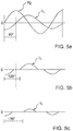
- FIGS 5a to 5c typical current wave forms for the inductor current I L with reference to the source voltage Vs are shown.
- the magnitude of the inductor current is dependent on the switch activation phase delay angle.
- the phase of the voltage source Vs is detected, for example by using a zero-crossing detector.
- the phase delay angle for switch activation in the following examples is measured from the detection of a Vs zero crossing.
- the delay angles are between 0° and 90°, as shown in Figure 5a
- the current is continuous so the maximum current flows through the inductor.
- the delay angle is between 90° and 180°
- the inductor current is discontinuous.
- the magnitude of the fundamental current I L1 flowing in the inductor reduces as the delay angle is increased.
- I L 1 V s ⁇ L 2 ⁇ ⁇ 2 ⁇ + sin 2 ⁇ where ( ⁇ /2 ⁇ ).
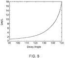
- FIG. 6 the relationship between the ratio of the effective or equivalent inductance to the actual inductance, and the delay angle, is shown.
- the equivalent inductance of the controlled inductor is equal to its self-inductance (i.e. the ratio is 1) when the delay angle is 90°.
- the equivalent inductance increases with corresponding increases in the delay angle.
- the inductor current would be zero, i.e. the equivalent inductance would be infinity. This is because the active switches will not be able to conduct since the applied voltage is negative.
- the equivalent inductance increases very sharply. This makes it unsuitable for a practical controller design.
- the harmonic components become larger compared to the fundamental current because of the large discontinuous period. As a consequence, the equation above becomes less accurate in calculating the equivalent inductance with increasing delay angles.
- control may be achieved by controlling the phase delay angle between approximately 90° and approximately 150°, since we have found that a delay angle over 150° is essentially equivalent to switching off the inductor.
- phase controlled variable inductor can be connected in series with the resonant track inductor, In practice the frequency control based on such a configuration is difficult to design, as the voltage source reference is not very stable and additional capacitors have to be put in parallel with the variable inductor to achieve effective control. We have found that placement of the variable inductor in parallel with the resonant tuning capacitor is a good option. Since the output of the inverting network Vac has a voltage source property and has very small harmonic components, it can be treated as the voltage reference Vs previously shown in Figure 4 . An example of one embodiment of a power supply including our variable inductor design is shown in Figure 7 . As shown in that figure, the phase controlled variable inductor is placed in parallel with the resonant capacitor.
- variable inductor is controlled so that when the delay angle is at 90° or less the inductor is completely "on" and the frequency of the system is at the high end of the available range. This is because the inductor cancels some capacitance of the tuning capacitor so the total equivalent capacitance reduces, resulting in a higher resonant frequency.
- the inductor when the delay angle is close to or over 180°, the inductor is effectively switched off so that the operating frequency of the system is at the lower end of the available range.
- 150° delay effectively defines the other end of the operating frequency range.
- the phase delay provides a predetermined time period before connection occurs in each half cycle, allowing control.
- variable inductor can be dynamically controlled by the switches S1 and S2 ( Figure 4 ) to change the delay angle and thus regulate the frequency to its normal or nominal value (or to a nominal value that may be selected). In this way, the undesirable effects of frequency change are substantially eliminated.
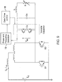
- the control mechanism is shown diagrammatically in figure 7 by phase detection unit 16 (which may comprise a zero-crossing detector) to detect zero crossings of the resonant circuit voltage and the direction of such crossings, or at least whether the voltage waveform is in the positive or negative half cycle. This information is supplied to the switch control unit 18.
- the zero crossing detection also provides a measurement of the frequency of the resonant circuit.
- control unit 18 which may include a microprocessor for controlling the switches (S1 and S2 in figure 4 ) across the variable inductor. Therefore, the frequency of the resonant circuit, as sensed, increases above the nominal resonant frequency of the circuit beyond a predetermined threshold then the phase delay angle is increased by a predetermined quantum to reduce the frequency.
- This control strategy may be implemented using techniques known to those skilled in the art.
- phase controlled variable inductor of the present invention was added in parallel with the parallel tuning capacitor. The results have shown that if the phase controlled inductor is designed such that at 120° delay, the system is running at its nominal 10 kHz, then at 90° delay the operating frequency is about 10.7 kHz and at 150° delay it is about 9.3 kHz. Under all the actual parameter variations and loading conditions range from no load to maximum load off this system, we have found that the operating frequency can be adjusted back to 10 kHz by changing the phase delay angle.
- a variable capacitance may be used as a variable reactive component to maintain the desired frequency of the resonant circuit in a converter. Therefore, an example of a further embodiment of a power supply according to the invention is shown in Figure 9 . Referring to that figure, circuit elements that are the same as or similar to those described with reference to the embodiment shown in Figure 7 , are labelled using the same reference numerals. As can be seen, the primary difference is the use of a variable capacitance 20, rather than a variable inductance.
- the controlled variable capacitor 20 may be placed in parallel with the resonant capacitor C. Alternatively, a variable capacitance may be used to completely replace the tuning capacitor.
- the variable capacitor includes a capacitor Cv and switches 24 and 26, which may be controlled to allow selected conduction of the capacitor Cv thus to vary the effective of capacitance of the tank circuit. Because the original tuning capacitor and the new variable capacitor Cv are in parallel, zero voltage switching techniques are preferably used to ensure smooth transients, as well as minimise the power losses and EMI. Detection means (not shown) detect current output by the supply shown in Figure 9 and this information is used by control means (not shown) to control switches 24 and 26 to dynamically vary the effective or equivalent capacitance and thus the frequency of the tank circuit. In this way the output frequency may be controlled to be substantially constant.
- variable capacitance Cv is arranged in parallel with the tuning capacitor C allows an adequate range of capacitance to be provided to allow reasonable control.
- the tuning capacitor C may be selected to be approximately one half of the capacitance actually required to provide resonance at the intended primary current frequency.
- the variable capacitor Cv may also comprise a capacitor of the same magnitude (i.e. one half of the capacitance required to provide resonance at the intended primary current frequency).
- the sum of the capacitance of tuning capacitor C and variable capacitor Cv is chosen to be greater than the capacitance required to provide the tank circuit with its desired natural resonant frequency (i.e. the nominal resonant frequency for the supply).
- variable capacitor Cv can be selectively “switched out” of the circuit to provide an overall equivalent capacitance for the circuit which allows it to operate at the nominal resonant frequency, if desired. Also, depending upon how "much" of the variable capacitor is effectively switched out of the circuit will allow the tank circuit to have a natural frequency which may be varied from below the nominal resonant frequency to some value above the nominal resonant frequency.
- Phase detector 16 and control unit 18 function in a similar way to their equivalents described above with reference to Figure 7 .
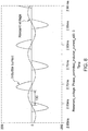
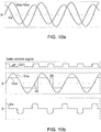
- Figures 10a and 10b show typical voltage and current waveforms of the controlled variable capacitor.
- the two switches that connect Cv to the circuit are always on, corresponding to the situation when the control phase angle (with reference to switching off) is zero electrical degrees, the current would be 90 electrical degrees leading the total resonant voltage across the two capacitors, as shown in Fig 10a .
- the phase angle is controlled between 0-90 degrees, capacitor Cv will be disconnected for a period.
- Figure 10b shows waveforms for the gate (switch) control signal, the voltage across Cv (Vcv), the voltage across Cs (Vcs), and the current through Cv (icv) for the situation when the phase angle is about 30 degrees.
- the switches When the switches are off, the voltage across Cv is kept constant and its current is zero.
- the switches When the switches are controlled to be on, its voltage is equal to the total resonant voltage and a current flows through capacitor Cv.
- the phase angle provides a predetermined time period before which disconnection occurs. If the phase angle is equal to or over 90 degrees, the capacitor is essentially off all the time. Therefore, by controlling the phase angle between 0 to 90 electrical degrees, the conduction period of the capacitor Cv is controlled, so the effective capacitance varies between its maximum value and zero.
- the invention may be used to energise a primary conductive path that may take a variety of different forms.
- a generally planar housing 30 is shown, within which a conductor 32 is disposed.
- the conductor 32 may be provided in the form of a loop or coil of conductive material.
- a number of turns of conductive material are provided and the conductor connection cables 34 exit the unit at an appropriate location to be connected to a power supply including a converter as described in one or more of the foregoing embodiments.
- the cables 34 may terminate in a plug or socket for electrical connection with a corresponding socket or plug associated with the power supply.
- the converter may be provided within the housing. Therefore, the housing may include external conductors for connection to a mains alternating current power supply, and a converter within the housing may rectify and filter the mains supply to provide an appropriate DC source which the converter then switches across the resonant circuit to provide the required AC supply for the conductor 32.
- the pad 30 may comprise a pad which is commonly used for a "point and click" device such as a mouse, or could comprise part of a desktop surface or similar surfaces.
- the housing 30 may be provided as part of a food tray or work surface (such as a folding food tray) in a vehicle such as an aircraft, train, bus or the like. Housing 30 could also be part of stone seats, wall tiles (used for heating) or towel rack (used for drying) in spas, saunas, bathrooms etc. It could be also used for animal cages to provide power to implants inside the animals such as rabbits, mice etc.
- the body of the housing is preferably constructed from a nonconductive material, but may include amorphous magnetic material 36 in one or more parts of the apparatus or in the apparatus as a whole. Such material can provide appropriate flux path(s) so that secondary devices may be placed in the vicinity of the housing 30, most preferably on the surface 38 of the housing, and be powered by mutual induction from the coil 32. Housing 30 can also work under water.
- Apparatus which may include secondary pickup devices for use in conjunction with the housing 30 may include a variety of devices which would normally be powered by one or more batteries, but may also include other devices for which it is convenient to have cordless operation. Such devices may include "point and click" devices (e.g. a mouse), cellular telephone devices, PDA's, notebooks or laptops, electric toothbrushes, electric shavers etc.
- These devices may include rechargeable cells or batteries of cells which the pickup recharges by power which is induced in the pickup coil from coil 32.
- the devices e.g. a mouse
- the devices may not require a battery as such because the device is only used in the vicinity of coil 32. Therefore the supply may be used to power battery and non-battery equipped pick-ups.
- the unit 30 may alternatively or in addition to conductor 32 include specific region for location of a device to which energy is to be supplied.
- one or more ferrite cores may be provided within the unit 30 with various markings on the upper surface 38 to indicate where a power receiving device should be placed.
- the upper surface 38 may be formed or contoured (for example by being appropriately moulded) to receive or accommodate the power receiving device. Therefore the invention is applicable to both loosely and closely coupled systems.
- the power supply provided by the invention allows this flexibility because the variations in load that occur as a result of coupling strength can be accommodated by the supply. If a "step-wise" approach is used for power supply frequency control, then load variations have to be limited to make the system function effectively.
- the use of the power supply embodiments discussed above to power the primary conductive path 32 has the advantage that a number of different devices may be placed on housing 30 to be powered by the coil 32. These multiple devices, which increase the load on the power supply, would normally tend to affect the power supply frequency.
- the dynamic tank circuit tuning provided by the invention means that multiple loads or changes in load do not affect system performance.
- the primary conductive path 32 within housing 30 may take a variety of different forms. In particular, a separate housing as such is not required. In some circumstances all that may be required is a conductor 32 which is provided in or on an underside of an appropriate surface such as a desktop for example. Also, rather than having the primary conductor arranged as a coil, a number of different configurations are possible. For example, a conductive path may be etched or printed on appropriate substrates such as a printed circuit board and the conductive path(s) may be arranged so as to provide a desired flux path or a plurality of desired flux paths which may be stationary or moving. For example, the flux paths may be designed to pad "rotate" so that a pick-up device may be placed in a variety of different positions or orientations adjacent to conductive path 32 and still receive sufficient energy to supply the required load.
- FIG 12 another embodiment of a primary conductive path for an ICPT power supply is shown.
- the primary conductive path is generally referenced 40, and a supplied by power supply 42 which may include a converter according to one or more of embodiments described above.
- the primary conductive path 40 may simply comprise a loop of conductive material. This material is preferably a multi-strand conductive material such as copper wire for example. However, as shown in figure 12 , it may be preferable in applications where pickups remain stationary relative to the primary conductive path 40 for the primary conductive path to be adapted to optimise power transfer to those pick-ups.
- An example of use of a primary conductive path to supply pick-ups that remain stationary relative to the path includes use of an ICPT system in a boat, a swimming pool or bath, a building, or a vehicle. To take the example of a boat, the primary conductive path may be provided in the boat during manufacture.
- the primary conductive path remains physically and electrically isolated so as not to be prone to damage and it is hidden so it does not interfere with the appearance of the structure. Power can be delivered to pick-up devices fitted in or on the boat without requiring the integrity of the boat structure to be compromised. In particular the hull does not need to be penetrated to install equipment such as depth or speed sensors. Alternatively, the primary conductive path may be retrofitted to a boat after manufacture.
- the primary conductive path may be modified in various predetermined positions about the boat structure. For example, in the vicinity of pickup 44 (which may comprise a navigation light for example), the conductive path may be widened at location 46 to provide an elongated or distributed region of increased magnetic field to facilitate power transfer to the pickup 44. Similarly, at location 48, one or more turns of conductive material may be included in the primary conductor (for example by looping the primary conductor) to facilitate data transfer to the pickup which may need a more significant energy requirement, for example an instrument panel that may be powered by pickup 50. Therefore a "hotspot" or region of relatively intense magnetic field strength is created.
- a further "hotspot” may be provided at location 52 in the primary conductive path for powering more than one pickup, such as pickups 54 and 56. If required, more than one "hotspot” may be provided as shown by regions 58 and 60 which can power a pickup 62 that has a more significant power requirement such as a battery charging device for example.
- regions 58 and 60 which can power a pickup 62 that has a more significant power requirement such as a battery charging device for example.
- simple elongated regions of primary conductive path that are unmodified, such as region 64 can be used to supply devices that may have a low power requirement and which may need to be moved about relative to the primary conductive path.
- the position of a navigation light supplied by pickup 66 and provided on the mast of the boat may need to be changed from time to time, so a simple length of primary conductor 64 may be provided on the mast of the boat, so that the pickup characteristic is uniform along the relevant portion of the mast.
- bioengineering applications such as implants for biological research or drug tests, waterproof applications, explosion proof applications, the mining industry (e.g. lights, sensors), the forestry industry (e.g. sensors), moving sensor applications (e.g. robots, optical sensors), heating systems (e.g. seat heating, towel drying).
- mining industry e.g. lights, sensors
- forestry industry e.g. sensors
- moving sensor applications e.g. robots, optical sensors
- heating systems e.g. seat heating, towel drying.
- the invention may be used to supply pick-ups that include batteries or which are battery-free.
- the pick-ups may include a super-capacitor as an energy storage device, which can be charge/discharged very quickly, and is very safe and almost maintenance free having a long life span..
- the invention provides a converter that has a frequency controlled resonant circuit, having advantages in a number of different applications, particularly ICPT power supplies for closely coupled or loosely coupled systems.
- the reactive element that is selectively phase controlled may comprise the circuit resonant element itself such as the converter tuning capacitor or the primary conductive path of an ICPT system.
- controlled variable reactive elements may be used in series tuned circuits as well as the parallel tuned circuits described by way of example above.
Landscapes
- Engineering & Computer Science (AREA)
- Power Engineering (AREA)
- Computer Networks & Wireless Communication (AREA)
- Inverter Devices (AREA)
- Dc-Dc Converters (AREA)
Claims (31)
- Resonanzwandler (2), aufweisend einen Eingang (4) zum Anschluss an eine im Wesentlichenelektrische Gleichstrom-Versorgung (Vd), einen Resonanzkreis, erste Schaltmittel zum selektiven Bereitstellen von Strom vom Eingang an den Resonanzkreis, zweite Schaltmittel (S1, S2), die einem reaktiven Element (Lv, Cv) des Resonanzkreises zugeordnet sind, und Schaltersteuermittel (18), die zum Steuern der zweiten Schaltmittel (S1, S2) betriebsfähig sind, um die effektive Reaktanz des reaktiven Elements (Lv, Cv) zu variieren, dadurch gekennzeichnet, dass Phasenerfassungsmittel (16) die Phase einer Spannung im Resonanzkreis erfassen, wodurch die Steuermittel (18) die zweiten Schaltmittel (S1, S2) betätigen können, um es dem reaktiven Element (Lv, Cv) zu ermöglichen, elektrisch an den Resonanzkreis angeschlossen oder davon getrennt zu werden, in einem vorbestimmten Zeitraum, nachdem das Phasenerfassungsmittel einen Spannungs-Nulldurchgang erfasst, um die effektive Reaktanz des reaktiven Elements (Lv, Cv) zu variieren und dadurch die Resonanzfrequenz des Resonanzkreises zu variieren.
- Resonanzwandler (2) nach Anspruch 1, wobei das reaktive Element einen Induktor (Lv) aufweist.
- Resonanzwandler (2) nach Anspruch 2, aufweisend Frequenzerfassungsmittel zum Erfassen der Frequenz des Resonanzkreises, wodurch die Steuermittel (18) die zweiten Schaltmittel (S1, S2) betätigen können, um es dem Induktor (Lv) zu ermöglichen, elektrisch an den Resonanzkreis angeschlossen oder davon getrennt zu werden, abhängig von der erfassten Frequenz, um die Frequenz des Resonanzkreises zu ändern.
- Resonanzwandler (2) nach Anspruch 2, wobei die Phasenerfassungsmittel (16) die Frequenz des Resonanzkreises erfassen, wodurch die Steuermittel (18) die zweiten Schaltmittel (S1, S2) betätigen können, um es dem Induktor (Lv) zu ermöglichen, elektrisch an den Resonanzkreis angeschlossen oder davon getrennt zu werden, abhängig von der erfassten Frequenz, um die Frequenz des Resonanzkreises zu ändern.
- Resonanzwandler (2) nach Anspruch 3 oder Anspruch 4, wobei das Steuermittel (18) betriebsfähig ist, um die erfasste Frequenz mit einer Nennfrequenz zu vergleichen und den vorbestimmten Zeitraum zu variieren, um die Frequenz des Resonanzkreises hin zur Nennfrequenz zu ändern.
- Resonanzwandler (2) nach Anspruch 5, wobei das Steuermittel (18) dafür ausgelegt ist, die zweiten Schaltmittel (S1, S2) zu aktivieren, um den Induktor (Lv) am Resonanzkreis anzuschließen, nach dem Verstreichen des vorbestimmten Zeitraums, der auf einen Spannungs-Nulldurchgang folgt, und es den zweiten Schaltmitteln (S1, S2) zu ermöglichen, deaktiviert zu werden, wenn die Spannung wieder im Wesentlichen null erreicht.
- Resonanzwandler (2) nach Anspruch 6, wobei das Steuermittel (18) in der Lage ist, den vorbestimmten Zeitraum zwischen im Wesentlichen 0 elektrischen Grad und im Wesentlichen 180 elektrischen Grad zu variieren, oder wobei das Steuermittel (18) in der Lage ist, den vorbestimmten Zeitraum zwischen im Wesentlichen 90 elektrischen Grad und im Wesentlichen 150 elektrischen Grad zu variieren.
- Resonanzwandler (2) nach einem der Ansprüche 2-7, wobei der Induktor (Lv) parallel zu einem Abstimmkondensator (C) des Resonanzkreises angeschlossen ist, oder wobei der Induktor (Lv) zwei Anschlussklemmen hat und die zweiten Schaltmittel (S1, S2) zwei steuerbare Halbleiter-Schaltelemente aufweisen, wobei ein Schaltelement zwischen jeder Anschlussklemme und dem Resonanzkreis angeschlossen ist, wobei vorzugsweise jedes Schaltelement eine quer darüber angeschlossene anti-parallele Diode (D1, D2) hat.
- Resonanzwandler (2) nach Anspruch 2, wobei der Induktor (Lv) eine primäre Leiterbahn eines induktiv gekoppelten Energieübertragungssystems (ICPT; inductively coupled power transfer) aufweist, oder wobei der Induktor (Lv) eine Induktionsheizspule eines Induktionsheizsystems aufweist.
- Resonanzwandler (2) nach Anspruch 1, wobei das reaktive Element (Lv, Cv) einen Kondensator (Cv) aufweist.
- Resonanzwandler (2) nach Anspruch 10, aufweisend Frequenzerfassungsmittel zum Erfassen der Frequenz des Resonanzkreises, wodurch die Steuermittel (18) die zweiten Schaltmittel (S1, S2) betätigen können, um es dem Kondensator (Cv) zu ermöglichen, elektrisch an den Resonanzkreis angeschlossen oder davon getrennt zu werden, abhängig von der erfassten Frequenz, um die Frequenz des Resonanzkreises zu ändern.
- Resonanzwandler (2) nach Anspruch 10, wobei die Phasenerfassungsmittel (16) die Frequenz des Resonanzkreises erfassen, wodurch die Steuermittel (18) die zweiten Schaltmittel (S1, S2) betätigen können, um es dem Kondensator (Cv) zu ermöglichen, elektrisch an den Resonanzkreis angeschlossen oder davon getrennt zu werden, abhängig von der erfassten Frequenz, um die Frequenz des Resonanzkreises zu ändern.
- Resonanzwandler (2) nach Anspruch 11 oder Anspruch 12, wobei das Steuermittel (18) betriebsfähig ist, um die erfasste Frequenz mit einer Nennfrequenz zu vergleichen und den vorbestimmten Zeitraum zu variieren, um die Frequenz des Resonanzkreises hin zur Nennfrequenz zu ändern.
- Resonanzwandler nach einem der Ansprüche 10 bis 13, wobei das Steuermittel (18) dafür ausgelegt ist, die zweiten Schaltmittel (S1, S2) zu aktivieren, um den Kondensator (Cv) vom Resonanzkreis zu trennen, nach dem Verstreichen des vorbestimmten Zeitraums, der auf einen Spannungs-Nulldurchgang folgt, und wobei das Steuermittel (18) in der Lage ist, den vorbestimmten Zeitraum zwischen im Wesentlichen 0 elektrischen Grad und im Wesentlichen 90 elektrischen Grad zu variieren.
- Resonanzwandler (2) nach einem der Ansprüche 12 bis 14, wobei der Kondensator (Cv) parallel zu einem Abstimmkondensator (C) des Resonanzkreises angeschlossen ist.
- Resonanzwandler (2) nach einem der Ansprüche 12 bis 15, wobei der Kondensator (Cv) zwei Anschlussklemmen hat und die zweiten Schaltmittel (S1, S2) zwei steuerbare Halbleiter-Schaltelemente aufweisen, wobei ein Schaltelement zwischen jeder Anschlussklemme und dem Resonanzkreis angeschlossen ist, und wobei jedes Schaltelement eine quer darüber angeschlossene anti-parallele Diode (D1, D2) hat.
- Resonanzwandler (2) nach Anspruch 8 oder Anspruch 16, wobei die Halbleiter-Schaltelemente IGBTs, MOSFETs, BJTs oder andere Halbleiter-Schalter umfassen.
- Resonanzwandler nach Anspruch 1, wobei der Wandler einen stromgespeisten Push-Pull-Resonanzwandler umfasst und der Resonanzkreis eine primäre Leiterbahn eines induktiv gekoppelten Energieübertragungssystems aufweist.
- Induktiv gekoppeltes Energieübertragungssystem, aufweisend:a. eine Energieversorgung, aufweisend einen Resonanzwandler nach Anspruch 1 mit einem Resonanzkreis, der eine primäre Leiterbahn eines induktiv gekoppelten Energieübertragungssystems aufweist;b. einen oder mehrere sekundäre Aufnahmekreise zum Empfangen von Energie von der primären Leiterbahn, wobei jede Aufnahme einen Aufnahme-Resonanzkreis hat, der eine Aufnahmespule und einen Abstimmkondensator aufweist, wodurch Energie von der primären Leiterbahn durch wechselseitige Induktion zwischen der primären Leiterbahn und der Spule an die Aufnahme übertragen werden kann.
- Induktiv gekoppeltes Energieübertragungssystem nach Anspruch 19, wobei die primäre Leiterbahn (6, 64) eine oder mehrere Windungen von elektrisch leitfähigem Material (32) aufweist, und wobei die primäre Leiterbahn (6) unterhalb einer im Wesentlichen planaren Oberfläche (38) vorgesehen ist.
- Induktiv gekoppeltes Energieübertragungssystem nach Anspruch 19, wobei die primäre Leiterbahn (6, 64) mindestens einen Bereich (48, 52, 58 60) aufweist, um den eine höhere Magnetfeldstärke als um einen oder mehrere andere Bereiche der Bahn besteht, oder wobei die primäre Leiterbahn eine oder mehrere konzentrierte Induktivitäten (48, 52) oder eine oder mehrere verteilte Induktivitäten (58, 60) aufweist.
- Induktiv gekoppeltes Energieübertragungssystem nach einem der Ansprüche 19 bis 21, wobei die primäre Leiterbahn (6, 64) benachbart zu einem amorphen magnetischen Material (36) angebracht ist, um einen gewünschten Magnetflussweg bereitzustellen.
- Induktiv gekoppeltes Energieübertragungssystem nach einem der Ansprüche 19 bis 22, wobei die Aufnahme (8, 44, 50, 54, 56, 62, 66) ein amorphes magnetisches Material (36) benachbart zur Aufnahmespule (10) aufweist, um einen gewünschten Magnetflussweg bereitzustellen.
- Induktiv gekoppeltes Energieübertragungssystem nach einem der Ansprüche 19 bis 23, wobei die Aufnahme (8, 44, 50, 54, 56, 62, 66) frei von Batterien ist, oder wobei die Aufnahme einen Superkondensator aufweist.
- Verfahren zur Frequenzstabilisierung für einen Resonanzwandler (2) mit einem Resonanzkreis, der ein induktives reaktives Element (L, Lv) und ein kapazitives reaktives Element (C, Cv) aufweist, dadurch gekennzeichnet, dass das Verfahren die Schritte des Erfassens der Phase einer Spannung im Resonanzkreis und des selektiven Schaltens eines der reaktiven Elemente in den oder aus dem Resonanzkreis aufweist, in einem vorbestimmten Zeitraum, nachdem das Phasenerfassungsmittel einen Spannungs-Nulldurchgang erfasst, um die effektive Induktivität oder Kapazität des reaktiven Elements zu ändern, um dadurch die Resonanzfrequenz des Resonanzkreises zu steuern.
- Verfahren nach Anspruch 25, wobei das Erfassen der Frequenz des Resonanzkreises ein Aktivieren eines Schaltmittels (S1, S2) aufweist, um das reaktive Element (S1, S2) elektrisch an den Resonanzkreis anzuschließen oder davon zu trennen, abhängig von der erfassten Frequenz, um die Frequenz des Resonanzkreises zu ändern.
- Verfahren nach Anspruch 25 oder Anspruch 26, aufweisend ein Vergleichen der erfassten Frequenz mit einer Nennfrequenz und ein Variieren des vorbestimmten Zeitraums, um die Frequenz des Resonanzkreises hin zur Nennfrequenz zu ändern.
- Verfahren nach einem der Ansprüche 25 bis 27, wobei das reaktive Element einen Induktor (Lv) aufweist und das Verfahren ein Aktivieren der Schaltmittel (S1, S2) aufweist, um das reaktive Element (Lv) an den Resonanzkreis anzuschließen, nachdem der vorbestimmte Zeitraum, der auf einen Spannungs-Nulldurchgang folgt verstrichen ist, und ein Ermöglichen für die zweiten Schaltmittel (S1, S2), deaktiviert zu werden, wenn die Spannung wieder im Wesentlichen null erreicht, und aufweisend ein Auswählen des vorbestimmten Zeitraums aus einem Bereich zwischen im Wesentlichen 0 elektrischen Grad und im Wesentlichen 180 elektrischen Grad.
- Verfahren nach Anspruch 28, aufweisend ein Auswählen des vorbestimmten Zeitraums aus einem Bereich zwischen im Wesentlichen 90 elektrischen Grad und im Wesentlichen 150 elektrischen Grad.
- Verfahren nach einem der Ansprüche 25 bis 27, wobei das reaktive Element einen Kondensator (Cv) aufweist und das Verfahren ein Aktivieren der Schaltmittel (S1, S2) aufweist, um das reaktive Element (Cv) vom Resonanzkreis zu trennen, nachdem der vorbestimmte Zeitraum, der auf einen Spannungs-Nulldurchgang folgt verstrichen ist, und wobei das Schaltmittel (S1, S2) das reaktive Element (Cv) an den Resonanzkreis anschließt, in einem vorbestimmten Intervall vor einem Spannungs-Nulldurchgang, wobei das vorbestimmte Intervall im Wesentlichen die gleiche Dauer wie der vorbestimmte Zeitraum hat.
- Verfahren nach Anspruch 30, aufweisend ein Auswählen des vorbestimmten Zeitraums aus einem Bereich zwischen 0 elektrischen Grad und 90 elektrischen Grad.
Applications Claiming Priority (3)
| Application Number | Priority Date | Filing Date | Title |
|---|---|---|---|
| NZ52611603 | 2003-05-23 | ||
| NZ52986903 | 2003-11-27 | ||
| PCT/NZ2004/000097 WO2004105226A1 (en) | 2003-05-23 | 2004-05-21 | Frequency controlled resonant converter |
Publications (3)
| Publication Number | Publication Date |
|---|---|
| EP1634366A1 EP1634366A1 (de) | 2006-03-15 |
| EP1634366A4 EP1634366A4 (de) | 2007-11-07 |
| EP1634366B1 true EP1634366B1 (de) | 2017-05-03 |
Family
ID=33479074
Family Applications (1)
| Application Number | Title | Priority Date | Filing Date |
|---|---|---|---|
| EP04734447.8A Expired - Lifetime EP1634366B1 (de) | 2003-05-23 | 2004-05-21 | Frequenzgeregelter resonanzwandler |
Country Status (7)
| Country | Link |
|---|---|
| US (2) | US8050068B2 (de) |
| EP (1) | EP1634366B1 (de) |
| JP (1) | JP4778432B2 (de) |
| CN (1) | CN1813396B (de) |
| AU (2) | AU2004241916A1 (de) |
| CA (1) | CA2526713C (de) |
| WO (1) | WO2004105226A1 (de) |
Cited By (1)
| Publication number | Priority date | Publication date | Assignee | Title |
|---|---|---|---|---|
| US11848632B2 (en) | 2020-08-28 | 2023-12-19 | Schneider Electric Industries Sas | Linear motor system and method for operating |
Families Citing this family (93)
| Publication number | Priority date | Publication date | Assignee | Title |
|---|---|---|---|---|
| US7522878B2 (en) | 1999-06-21 | 2009-04-21 | Access Business Group International Llc | Adaptive inductive power supply with communication |
| US7212414B2 (en) | 1999-06-21 | 2007-05-01 | Access Business Group International, Llc | Adaptive inductive power supply |
| US7385357B2 (en) * | 1999-06-21 | 2008-06-10 | Access Business Group International Llc | Inductively coupled ballast circuit |
| NZ535390A (en) | 2004-09-16 | 2007-10-26 | Auckland Uniservices Ltd | Inductively powered mobile sensor system |
| TWI265364B (en) * | 2005-04-08 | 2006-11-01 | Delta Electronics Inc | Switching system and switching method thereof |
| NZ539771A (en) * | 2005-04-29 | 2007-10-26 | Auckland Uniservices Ltd | Tuning methods and apparatus for inductively coupled power transfer (ICPT) systems |
| NZ541629A (en) * | 2005-08-03 | 2008-02-29 | Auckland Uniservices Ltd | Resonant inverter which includes two or more inductive elements that form part of a resonant circuit of the inverter |
| TW200733523A (en) * | 2005-10-25 | 2007-09-01 | Koninkl Philips Electronics Nv | Power converter |
| US7952322B2 (en) | 2006-01-31 | 2011-05-31 | Mojo Mobility, Inc. | Inductive power source and charging system |
| US8169185B2 (en) | 2006-01-31 | 2012-05-01 | Mojo Mobility, Inc. | System and method for inductive charging of portable devices |
| US11201500B2 (en) | 2006-01-31 | 2021-12-14 | Mojo Mobility, Inc. | Efficiencies and flexibilities in inductive (wireless) charging |
| CN101427452B (zh) | 2006-04-25 | 2012-10-03 | 皇家飞利浦电子股份有限公司 | 用于确定开关点的电力逆变器控制设备 |
| NZ547604A (en) * | 2006-05-30 | 2008-09-26 | John Talbot Boys | Inductive power transfer system pick-up circuit |
| US11329511B2 (en) | 2006-06-01 | 2022-05-10 | Mojo Mobility Inc. | Power source, charging system, and inductive receiver for mobile devices |
| US7948208B2 (en) | 2006-06-01 | 2011-05-24 | Mojo Mobility, Inc. | Power source, charging system, and inductive receiver for mobile devices |
| HUE053507T2 (hu) * | 2006-12-20 | 2021-07-28 | Primozone Production Ab | Nagyfeszültségû transzformátor |
| US10069341B2 (en) | 2007-08-21 | 2018-09-04 | Auckland Uniservices Limited | Inductively powered mobile sensor system |
| JP2009201211A (ja) * | 2008-02-20 | 2009-09-03 | Asyst Technologies Japan Inc | 電力供給システム |
| US20110050164A1 (en) | 2008-05-07 | 2011-03-03 | Afshin Partovi | System and methods for inductive charging, and improvements and uses thereof |
| GB2461578A (en) | 2008-07-04 | 2010-01-06 | Bombardier Transp Gmbh | Transferring electric energy to a vehicle |
| GB2461577A (en) | 2008-07-04 | 2010-01-06 | Bombardier Transp Gmbh | System and method for transferring electric energy to a vehicle |
| JP4911148B2 (ja) * | 2008-09-02 | 2012-04-04 | ソニー株式会社 | 非接触給電装置 |
| WO2010027282A2 (en) * | 2008-09-05 | 2010-03-11 | Fisher & Paykel Healthcare Limited | Contactless power transfer in a system for providing respiratory gases to a user for therapeutic purposes |
| KR101710147B1 (ko) * | 2008-09-11 | 2017-02-24 | 오클랜드 유니서비시즈 리미티드 | 유도 결합 ac 전력 전송 |
| GB2463692A (en) | 2008-09-19 | 2010-03-24 | Bombardier Transp Gmbh | An arrangement for providing a vehicle with electric energy |
| GB2463693A (en) | 2008-09-19 | 2010-03-24 | Bombardier Transp Gmbh | A system for transferring electric energy to a vehicle |
| JP5174628B2 (ja) * | 2008-11-20 | 2013-04-03 | オリンパス株式会社 | 電力供給装置 |
| CA2752573A1 (en) * | 2009-02-13 | 2010-08-19 | Witricity Corporation | Wireless energy transfer in lossy environments |
| JP5533856B2 (ja) | 2009-03-30 | 2014-06-25 | 富士通株式会社 | 無線電力供給システム、無線送電装置、および無線受電装置 |
| IN2012DN01947A (de) * | 2009-08-07 | 2015-08-21 | Auckland Uniservices Ltd | |
| WO2011033660A1 (ja) * | 2009-09-18 | 2011-03-24 | 株式会社 東芝 | 無線電力伝送装置 |
| JP5691458B2 (ja) * | 2010-03-31 | 2015-04-01 | 日産自動車株式会社 | 非接触給電装置及び非接触給電方法 |
| JP6144195B2 (ja) * | 2010-05-19 | 2017-07-12 | オークランド ユニサービシズ リミテッドAuckland Uniservices Limited | 誘導電力転送システム1次トラックトポロジー |
| EP2580844A4 (de) | 2010-06-11 | 2016-05-25 | Mojo Mobility Inc | Interoperabilität unterstützendes system für drahtlose stromübertragung sowie mehrpolige magneten zur verwendung damit |
| US9356659B2 (en) | 2011-01-18 | 2016-05-31 | Mojo Mobility, Inc. | Chargers and methods for wireless power transfer |
| US11342777B2 (en) | 2011-01-18 | 2022-05-24 | Mojo Mobility, Inc. | Powering and/or charging with more than one protocol |
| US9496732B2 (en) | 2011-01-18 | 2016-11-15 | Mojo Mobility, Inc. | Systems and methods for wireless power transfer |
| US9178369B2 (en) | 2011-01-18 | 2015-11-03 | Mojo Mobility, Inc. | Systems and methods for providing positioning freedom, and support of different voltages, protocols, and power levels in a wireless power system |
| US10115520B2 (en) | 2011-01-18 | 2018-10-30 | Mojo Mobility, Inc. | Systems and method for wireless power transfer |
| DE102011016027A1 (de) | 2011-04-04 | 2012-10-04 | Markus Rehm | Großsignal VCO |
| JP5338862B2 (ja) | 2011-06-29 | 2013-11-13 | 株式会社ダイフク | 無接触給電設備 |
| KR20130039031A (ko) * | 2011-10-11 | 2013-04-19 | 한국전자통신연구원 | 무선 전력 송신 장치, 무선 전력 수신 장치 그리고 무선 전력 송수신 장치 |
| JP6005170B2 (ja) * | 2011-10-21 | 2016-10-12 | クアルコム,インコーポレイテッド | 受動負荷の静的または動的調整のための負荷インピーダンス検出 |
| US9647572B2 (en) | 2011-11-10 | 2017-05-09 | Powerbyproxi Limited | Method for controlling a converter |
| EP2798730B1 (de) | 2011-12-28 | 2017-11-08 | DET International Holding Limited | Bidirektionaler resonanter gleichstrom-wechselstrom-umrichter |
| JP5696058B2 (ja) | 2012-01-13 | 2015-04-08 | 株式会社東芝 | 受電装置、送電装置および制御装置 |
| CN103259429A (zh) * | 2012-02-16 | 2013-08-21 | 阳光电源股份有限公司 | 一种逆变电源装置 |
| US9998179B2 (en) * | 2012-03-09 | 2018-06-12 | Auckland Uniservices Limited | Shorting period control in inductive power transfer systems |
| US9722447B2 (en) | 2012-03-21 | 2017-08-01 | Mojo Mobility, Inc. | System and method for charging or powering devices, such as robots, electric vehicles, or other mobile devices or equipment |
| US9196417B2 (en) | 2012-05-04 | 2015-11-24 | Det International Holding Limited | Magnetic configuration for high efficiency power processing |
| US9494631B2 (en) * | 2012-05-04 | 2016-11-15 | Det International Holding Limited | Intelligent current analysis for resonant converters |
| EP3264564A1 (de) | 2012-05-04 | 2018-01-03 | DET International Holding Limited | Mehrfachresonanzzellen für induktive ladekissen |
| US20130314188A1 (en) | 2012-05-04 | 2013-11-28 | Ionel Jitaru | Magnetic Structure for Large Air Gap |
| US10553351B2 (en) | 2012-05-04 | 2020-02-04 | Delta Electronics (Thailand) Public Co., Ltd. | Multiple cells magnetic structure for wireless power |
| JP6525874B2 (ja) * | 2012-08-31 | 2019-06-05 | オークランド ユニサービシズ リミテッドAuckland Uniservices Limited | 効率の改善された非自己同調無線電力伝送システム |
| JP5741962B2 (ja) | 2012-11-30 | 2015-07-01 | 株式会社デンソー | 非接触給電装置 |
| US9837846B2 (en) | 2013-04-12 | 2017-12-05 | Mojo Mobility, Inc. | System and method for powering or charging receivers or devices having small surface areas or volumes |
| JP2016535578A (ja) | 2013-08-19 | 2016-11-10 | ハートウェア,インコーポレイテッド | マルチバンドワイヤレス電力システム |
| CN104426358B (zh) * | 2013-09-05 | 2020-02-21 | 联想(北京)有限公司 | 一种供电电路以及电子设备 |
| JP6450766B2 (ja) * | 2013-09-12 | 2019-01-09 | オークランド ユニサービシズ リミテッドAuckland Uniservices Limited | 自己同調を有する共振電力供給 |
| US10236720B2 (en) | 2013-09-26 | 2019-03-19 | Semiconductor Components Industries, Llc | Wireless power transfer system and driving method thereof |
| WO2015084587A1 (en) | 2013-12-03 | 2015-06-11 | Massachusetts Institute Of Technology | Method and apparatus for wirelessly charging portable electronic devices |
| CN106062906B (zh) * | 2014-01-22 | 2019-06-04 | 苹果公司 | 感应功率传输装置及其控制方法 |
| JP6356437B2 (ja) * | 2014-03-03 | 2018-07-11 | 東海旅客鉄道株式会社 | 受電装置 |
| DE102014205598A1 (de) * | 2014-03-26 | 2015-10-01 | Robert Bosch Gmbh | Überwachungsvorrichtung für mindestens eine zur induktiven Energieübertragung ausgelegte elektrische Vorrichtung und Verfahren zum Überwachen zumindest einer Teilumgebung mindestens einer zur induktiven Energieübertragung ausgelegten elektrischen Vorrichtung |
| US9866280B2 (en) | 2014-05-23 | 2018-01-09 | Samsung Electronics Co., Ltd. | Mobile communication device with wireless communications unit and wireless power receiver |
| US9977858B2 (en) * | 2014-07-03 | 2018-05-22 | The Boeing Company | Electromagnetic interference filters for power converter applications |
| US10149933B2 (en) | 2014-07-25 | 2018-12-11 | Minnetronix, Inc. | Coil parameters and control |
| US9855376B2 (en) | 2014-07-25 | 2018-01-02 | Minnetronix, Inc. | Power scaling |
| US10521041B2 (en) * | 2014-08-13 | 2019-12-31 | Texas Instruments Incorporated | Resonant line driver including energy transfer inductor for driving capacitive-load lines |
| US20170279313A1 (en) * | 2014-08-21 | 2017-09-28 | Powerbyproxi Limited | Inductive power transmitter |
| US20160065088A1 (en) * | 2014-08-28 | 2016-03-03 | Shenzhen Wisepower Innovation Technology Co., Ltd | Push pull inverter |
| US10342908B2 (en) | 2015-01-14 | 2019-07-09 | Minnetronix, Inc. | Distributed transformer |
| US10406267B2 (en) | 2015-01-16 | 2019-09-10 | Minnetronix, Inc. | Data communication in a transcutaneous energy transfer system |
| DE102016106657A1 (de) | 2015-04-14 | 2016-10-20 | Minnetronix, Inc. | Repeater-resonanzkreis |
| US10498160B2 (en) | 2015-08-03 | 2019-12-03 | Massachusetts Institute Of Technology | Efficiency maximization for device-to-device wireless charging |
| KR102612384B1 (ko) * | 2016-02-08 | 2023-12-12 | 위트리시티 코포레이션 | Pwm 커패시터 제어 |
| US9979273B2 (en) | 2016-05-19 | 2018-05-22 | Abb Schweiz Ag | Resonant converters with variable inductor |
| WO2018048312A1 (en) | 2016-09-06 | 2018-03-15 | Powerbyproxi Limited | An inductive power transmitter |
| SG10201708314TA (en) * | 2016-10-28 | 2018-05-30 | Gen Electric | System and method for actively controlling output voltage of a wireless power transfer system |
| CN110999029A (zh) | 2017-05-30 | 2020-04-10 | 无线先进车辆电气化有限公司 | 单点馈电多垫式无线充电 |
| FR3077439B1 (fr) * | 2018-01-31 | 2020-11-20 | Valeo Equip Electr Moteur | Dispositif de transmission de puissance sans contact par couplage inductif a resonance pour recharger un vehicule automobile |
| US11018526B2 (en) | 2018-02-08 | 2021-05-25 | Massachusetts Institute Of Technology | Detuning for a resonant wireless power transfer system including cooperative power sharing |
| US10651687B2 (en) | 2018-02-08 | 2020-05-12 | Massachusetts Institute Of Technology | Detuning for a resonant wireless power transfer system including cryptography |
| EP3644484A1 (de) * | 2018-10-25 | 2020-04-29 | ABB Schweiz AG | Stromrichteranordnung mit dämpfungselement für elektrisches überschwingen |
| CN109546759A (zh) * | 2018-12-26 | 2019-03-29 | 北京酷能科技有限公司 | 谐波电流抑制电路 |
| US11444485B2 (en) | 2019-02-05 | 2022-09-13 | Mojo Mobility, Inc. | Inductive charging system with charging electronics physically separated from charging coil |
| JP7341249B2 (ja) * | 2019-03-15 | 2023-09-08 | ヴァレオ エキプマン エレクトリク モトゥール | 自動車両を再充電するために共振誘導結合を介して非接触で電力を伝送する装置 |
| CN110816321B (zh) * | 2019-08-12 | 2022-11-11 | 华为技术有限公司 | 一种无线充电发射装置,发射方法及无线充电系统 |
| WO2021137065A1 (en) * | 2019-12-30 | 2021-07-08 | Folquer Holdings Limited | An electric power system and a method of transmitting electric power from a power source to a device via a single-wire |
| GB2597735B (en) * | 2020-07-31 | 2024-06-26 | Energy Res Lab Ltd | Power supply apparatus |
| EP4189822A1 (de) | 2020-07-31 | 2023-06-07 | Energy Research Lab Ltd | Wechselrichter |
| CN115173664B (zh) * | 2022-07-15 | 2025-08-29 | 东南大学 | 基于时变磁感原理的发电装置及方法 |
Family Cites Families (24)
| Publication number | Priority date | Publication date | Assignee | Title |
|---|---|---|---|---|
| US5075599A (en) | 1989-11-29 | 1991-12-24 | U.S. Philips Corporation | Circuit arrangement |
| JP2961897B2 (ja) * | 1990-12-10 | 1999-10-12 | 日本電気株式会社 | スイッチング電源装置 |
| US5293308A (en) * | 1991-03-26 | 1994-03-08 | Auckland Uniservices Limited | Inductive power distribution system |
| US5450305A (en) * | 1991-08-12 | 1995-09-12 | Auckland Uniservices Limited | Resonant power supplies |
| EP0640254B1 (de) * | 1992-05-10 | 2001-08-01 | Auckland Uniservices Limited | System zur berührungslosen energieübertragung |
| GB2293702A (en) | 1994-09-27 | 1996-04-03 | Marconi Gec Ltd | Contactless electrical power coupling and converter |
| US5953642A (en) * | 1994-10-26 | 1999-09-14 | Siemens Aktiengesellschaft | System for contactless power and data transmission |
| DE4438286C2 (de) * | 1994-10-26 | 2002-09-12 | Siemens Ag | System zur kontaktlosen Energie- und Datenübertragung |
| US5684678A (en) * | 1995-12-08 | 1997-11-04 | Delco Electronics Corp. | Resonant converter with controlled inductor |
| DE19621076C2 (de) | 1996-05-24 | 2001-06-28 | Siemens Ag | Vorrichtung und Verfahren zum kontaktlosen Übertragen von Energie oder Daten |
| JPH09326736A (ja) * | 1996-06-03 | 1997-12-16 | Mitsubishi Electric Corp | ワイヤレス送受信システム用2次側回路装置およびワイヤレス送受信システム用誘導コイル |
| WO1998034319A1 (fr) * | 1997-02-03 | 1998-08-06 | Sony Corporation | Equipement et procede pour le transfert d'energie electrique |
| DE19735624C1 (de) * | 1997-08-18 | 1998-12-10 | Daimler Benz Ag | Verfahren und Anordnung zur induktiven Übertragung elektrischer Leistung auf mehrere bewegte Verbraucher |
| NZ329195A (en) | 1997-11-17 | 2000-07-28 | Auckland Uniservices Ltd | Loosely coupled inductive power transfer using resonant pickup circuit, inductor core chosen to saturate under overload conditions |
| US5909362A (en) * | 1998-01-12 | 1999-06-01 | Eldec Corporation | Resonant power converter |
| US6173899B1 (en) * | 1998-04-03 | 2001-01-16 | Alexander Rozin | Method and system for contactless energy transmission and data exchange between a terminal and IC card |
| JP2000116145A (ja) | 1998-09-29 | 2000-04-21 | Denso Corp | 共振形電力変換装置 |
| US7212414B2 (en) * | 1999-06-21 | 2007-05-01 | Access Business Group International, Llc | Adaptive inductive power supply |
| NZ337716A (en) | 1999-09-09 | 2002-10-25 | Auckland Uniservices Ltd | Series resonant inductive pickup where power can be regulated by time-regulated opening and closing a switch |
| DE19961228A1 (de) * | 1999-12-18 | 2001-06-28 | Philips Corp Intellectual Pty | Konverter mit Resonanzkreiselementen |
| JP4021151B2 (ja) * | 2001-03-06 | 2007-12-12 | 株式会社東芝 | 誘導加熱調理器 |
| US6430064B1 (en) * | 2001-06-29 | 2002-08-06 | Aichi Electric Co. Ltd. | Non-contact power supply device |
| US6487095B1 (en) * | 2001-10-31 | 2002-11-26 | International Business Machines Corporation | Multiphase zero-volt-switching resonant DC-DC regulator |
| US6906495B2 (en) | 2002-05-13 | 2005-06-14 | Splashpower Limited | Contact-less power transfer |
-
2004
- 2004-05-21 EP EP04734447.8A patent/EP1634366B1/de not_active Expired - Lifetime
- 2004-05-21 CN CN2004800181548A patent/CN1813396B/zh not_active Expired - Lifetime
- 2004-05-21 JP JP2006532160A patent/JP4778432B2/ja not_active Expired - Lifetime
- 2004-05-21 US US10/558,338 patent/US8050068B2/en active Active
- 2004-05-21 AU AU2004241916A patent/AU2004241916A1/en not_active Abandoned
- 2004-05-21 WO PCT/NZ2004/000097 patent/WO2004105226A1/en not_active Ceased
- 2004-05-21 CA CA2526713A patent/CA2526713C/en not_active Expired - Lifetime
-
2010
- 2010-11-10 AU AU2010241353A patent/AU2010241353B2/en not_active Expired
-
2011
- 2011-08-11 US US13/208,020 patent/US20110299313A1/en not_active Abandoned
Non-Patent Citations (1)
| Title |
|---|
| None * |
Cited By (1)
| Publication number | Priority date | Publication date | Assignee | Title |
|---|---|---|---|---|
| US11848632B2 (en) | 2020-08-28 | 2023-12-19 | Schneider Electric Industries Sas | Linear motor system and method for operating |
Also Published As
| Publication number | Publication date |
|---|---|
| JP2006529079A (ja) | 2006-12-28 |
| WO2004105226A1 (en) | 2004-12-02 |
| US8050068B2 (en) | 2011-11-01 |
| AU2004241916A1 (en) | 2004-12-02 |
| AU2010241353A1 (en) | 2010-12-02 |
| EP1634366A1 (de) | 2006-03-15 |
| CN1813396B (zh) | 2010-04-28 |
| CN1813396A (zh) | 2006-08-02 |
| US20110299313A1 (en) | 2011-12-08 |
| CA2526713C (en) | 2012-10-02 |
| EP1634366A4 (de) | 2007-11-07 |
| US20080211478A1 (en) | 2008-09-04 |
| AU2010241353B2 (en) | 2011-10-06 |
| JP4778432B2 (ja) | 2011-09-21 |
| CA2526713A1 (en) | 2004-12-02 |
Similar Documents
| Publication | Publication Date | Title |
|---|---|---|
| EP1634366B1 (de) | Frequenzgeregelter resonanzwandler | |
| EP1634355B1 (de) | Verfahren und vorrichtungen zur steuerung induktiv gekoppelter energietransfersysteme | |
| US7310245B2 (en) | Electric power transmission device and electric power transmission method | |
| Samanta et al. | A new inductive power transfer topology using direct AC–AC converter with active source current waveshaping | |
| Jang et al. | A contactless electrical energy transmission system for portable-telephone battery chargers | |
| US7781916B2 (en) | Parallel-tuned pick-up system with multiple voltage outputs | |
| EP1858146A1 (de) | Gleichstrom-gleichstrom-wandler | |
| WO2000057543A8 (en) | High frequency switch-mode dc powered computer system | |
| KR20110110783A (ko) | 단상과 3상 동작을 위한 컨버터, dc 전압원 및 배터리충전기 | |
| NZ526115A (en) | Methods and apparatus for detuning a pick-up of a contactless power supply | |
| KR20120069349A (ko) | 스위칭 손실을 줄이는 직류-직류 전압 변환기, 상기 직류-직류 전압 변환기를 포함하는 무선전력 수신 장치 | |
| US9054602B2 (en) | Resonant circuit with constant current characteristics | |
| AU2011265542A1 (en) | Frequency controlled resonant converter | |
| JP2009254031A (ja) | 非接触給電装置 | |
| JP2010136519A (ja) | 非接触給電装置 | |
| Gunji et al. | Operating point setting method for wireless power transfer with constant voltage load | |
| US20250373083A1 (en) | Switch configuration control for wireless charging circuits | |
| Jang et al. | A new soft-switched contactless battery charger with robust local controllers | |
| US20250357799A1 (en) | Switching circuits to reduce leakage current in inductive charging | |
| CN120958686A (zh) | 非接触受电装置、非接触供电系统及其方法 | |
| Rodriguez et al. | Capability analysis for an inductively coupled power transfer system |
Legal Events
| Date | Code | Title | Description |
|---|---|---|---|
| PUAI | Public reference made under article 153(3) epc to a published international application that has entered the european phase |
Free format text: ORIGINAL CODE: 0009012 |
|
| 17P | Request for examination filed |
Effective date: 20051223 |
|
| AK | Designated contracting states |
Kind code of ref document: A1 Designated state(s): AT BE BG CH CY CZ DE DK EE ES FI FR GB GR HU IE IT LI LU MC NL PL PT RO SE SI SK TR |
|
| AX | Request for extension of the european patent |
Extension state: AL LT LV MK |
|
| RAX | Requested extension states of the european patent have changed |
Extension state: LT Payment date: 20051223 Extension state: MK Payment date: 20051223 Extension state: AL Payment date: 20051223 Extension state: LV Payment date: 20051223 |
|
| A4 | Supplementary search report drawn up and despatched |
Effective date: 20071005 |
|
| 17Q | First examination report despatched |
Effective date: 20080121 |
|
| RIC1 | Information provided on ipc code assigned before grant |
Ipc: H02M 7/217 20060101AFI20150804BHEP Ipc: H02M 3/337 20060101ALI20150804BHEP |
|
| REG | Reference to a national code |
Ref country code: DE Ref legal event code: R079 Ref document number: 602004051198 Country of ref document: DE Free format text: PREVIOUS MAIN CLASS: H02M0007523000 Ipc: H02M0007480000 |
|
| GRAJ | Information related to disapproval of communication of intention to grant by the applicant or resumption of examination proceedings by the epo deleted |
Free format text: ORIGINAL CODE: EPIDOSDIGR1 |
|
| GRAP | Despatch of communication of intention to grant a patent |
Free format text: ORIGINAL CODE: EPIDOSNIGR1 |
|
| RIC1 | Information provided on ipc code assigned before grant |
Ipc: H02M 7/48 20070101AFI20161220BHEP Ipc: H02J 50/12 20160101ALI20161220BHEP Ipc: H02M 3/337 20060101ALI20161220BHEP |
|
| GRAP | Despatch of communication of intention to grant a patent |
Free format text: ORIGINAL CODE: EPIDOSNIGR1 |
|
| INTG | Intention to grant announced |
Effective date: 20170208 |
|
| GRAS | Grant fee paid |
Free format text: ORIGINAL CODE: EPIDOSNIGR3 |
|
| GRAA | (expected) grant |
Free format text: ORIGINAL CODE: 0009210 |
|
| AK | Designated contracting states |
Kind code of ref document: B1 Designated state(s): AT BE BG CH CY CZ DE DK EE ES FI FR GB GR HU IE IT LI LU MC NL PL PT RO SE SI SK TR |
|
| AX | Request for extension of the european patent |
Extension state: AL LT LV MK |
|
| REG | Reference to a national code |
Ref country code: GB Ref legal event code: FG4D |
|
| REG | Reference to a national code |
Ref country code: AT Ref legal event code: REF Ref document number: 891014 Country of ref document: AT Kind code of ref document: T Effective date: 20170515 Ref country code: CH Ref legal event code: EP |
|
| REG | Reference to a national code |
Ref country code: IE Ref legal event code: FG4D |
|
| REG | Reference to a national code |
Ref country code: DE Ref legal event code: R096 Ref document number: 602004051198 Country of ref document: DE |
|
| REG | Reference to a national code |
Ref country code: FR Ref legal event code: PLFP Year of fee payment: 14 |
|
| REG | Reference to a national code |
Ref country code: NL Ref legal event code: MP Effective date: 20170503 |
|
| REG | Reference to a national code |
Ref country code: AT Ref legal event code: MK05 Ref document number: 891014 Country of ref document: AT Kind code of ref document: T Effective date: 20170503 |
|
| REG | Reference to a national code |
Ref country code: LT Ref legal event code: MG9D |
|
| PG25 | Lapsed in a contracting state [announced via postgrant information from national office to epo] |
Ref country code: AT Free format text: LAPSE BECAUSE OF FAILURE TO SUBMIT A TRANSLATION OF THE DESCRIPTION OR TO PAY THE FEE WITHIN THE PRESCRIBED TIME-LIMIT Effective date: 20170503 Ref country code: FI Free format text: LAPSE BECAUSE OF FAILURE TO SUBMIT A TRANSLATION OF THE DESCRIPTION OR TO PAY THE FEE WITHIN THE PRESCRIBED TIME-LIMIT Effective date: 20170503 Ref country code: GR Free format text: LAPSE BECAUSE OF FAILURE TO SUBMIT A TRANSLATION OF THE DESCRIPTION OR TO PAY THE FEE WITHIN THE PRESCRIBED TIME-LIMIT Effective date: 20170804 Ref country code: ES Free format text: LAPSE BECAUSE OF FAILURE TO SUBMIT A TRANSLATION OF THE DESCRIPTION OR TO PAY THE FEE WITHIN THE PRESCRIBED TIME-LIMIT Effective date: 20170503 |
|
| PG25 | Lapsed in a contracting state [announced via postgrant information from national office to epo] |
Ref country code: SE Free format text: LAPSE BECAUSE OF FAILURE TO SUBMIT A TRANSLATION OF THE DESCRIPTION OR TO PAY THE FEE WITHIN THE PRESCRIBED TIME-LIMIT Effective date: 20170503 Ref country code: PL Free format text: LAPSE BECAUSE OF FAILURE TO SUBMIT A TRANSLATION OF THE DESCRIPTION OR TO PAY THE FEE WITHIN THE PRESCRIBED TIME-LIMIT Effective date: 20170503 Ref country code: NL Free format text: LAPSE BECAUSE OF FAILURE TO SUBMIT A TRANSLATION OF THE DESCRIPTION OR TO PAY THE FEE WITHIN THE PRESCRIBED TIME-LIMIT Effective date: 20170503 Ref country code: BG Free format text: LAPSE BECAUSE OF FAILURE TO SUBMIT A TRANSLATION OF THE DESCRIPTION OR TO PAY THE FEE WITHIN THE PRESCRIBED TIME-LIMIT Effective date: 20170803 |
|
| REG | Reference to a national code |
Ref country code: CH Ref legal event code: PL |
|
| PG25 | Lapsed in a contracting state [announced via postgrant information from national office to epo] |
Ref country code: DK Free format text: LAPSE BECAUSE OF FAILURE TO SUBMIT A TRANSLATION OF THE DESCRIPTION OR TO PAY THE FEE WITHIN THE PRESCRIBED TIME-LIMIT Effective date: 20170503 Ref country code: EE Free format text: LAPSE BECAUSE OF FAILURE TO SUBMIT A TRANSLATION OF THE DESCRIPTION OR TO PAY THE FEE WITHIN THE PRESCRIBED TIME-LIMIT Effective date: 20170503 Ref country code: CZ Free format text: LAPSE BECAUSE OF FAILURE TO SUBMIT A TRANSLATION OF THE DESCRIPTION OR TO PAY THE FEE WITHIN THE PRESCRIBED TIME-LIMIT Effective date: 20170503 Ref country code: SK Free format text: LAPSE BECAUSE OF FAILURE TO SUBMIT A TRANSLATION OF THE DESCRIPTION OR TO PAY THE FEE WITHIN THE PRESCRIBED TIME-LIMIT Effective date: 20170503 Ref country code: RO Free format text: LAPSE BECAUSE OF FAILURE TO SUBMIT A TRANSLATION OF THE DESCRIPTION OR TO PAY THE FEE WITHIN THE PRESCRIBED TIME-LIMIT Effective date: 20170503 |
|
| REG | Reference to a national code |
Ref country code: DE Ref legal event code: R097 Ref document number: 602004051198 Country of ref document: DE |
|
| REG | Reference to a national code |
Ref country code: IE Ref legal event code: MM4A |
|
| PG25 | Lapsed in a contracting state [announced via postgrant information from national office to epo] |
Ref country code: LI Free format text: LAPSE BECAUSE OF NON-PAYMENT OF DUE FEES Effective date: 20170531 Ref country code: CH Free format text: LAPSE BECAUSE OF NON-PAYMENT OF DUE FEES Effective date: 20170531 |
|
| PLBE | No opposition filed within time limit |
Free format text: ORIGINAL CODE: 0009261 |
|
| STAA | Information on the status of an ep patent application or granted ep patent |
Free format text: STATUS: NO OPPOSITION FILED WITHIN TIME LIMIT |
|
| PG25 | Lapsed in a contracting state [announced via postgrant information from national office to epo] |
Ref country code: LU Free format text: LAPSE BECAUSE OF NON-PAYMENT OF DUE FEES Effective date: 20170521 |
|
| 26N | No opposition filed |
Effective date: 20180206 |
|
| REG | Reference to a national code |
Ref country code: BE Ref legal event code: MM Effective date: 20170531 |
|
| PG25 | Lapsed in a contracting state [announced via postgrant information from national office to epo] |
Ref country code: IE Free format text: LAPSE BECAUSE OF NON-PAYMENT OF DUE FEES Effective date: 20170521 |
|
| REG | Reference to a national code |
Ref country code: FR Ref legal event code: PLFP Year of fee payment: 15 |
|
| PG25 | Lapsed in a contracting state [announced via postgrant information from national office to epo] |
Ref country code: SI Free format text: LAPSE BECAUSE OF FAILURE TO SUBMIT A TRANSLATION OF THE DESCRIPTION OR TO PAY THE FEE WITHIN THE PRESCRIBED TIME-LIMIT Effective date: 20170503 |
|
| PG25 | Lapsed in a contracting state [announced via postgrant information from national office to epo] |
Ref country code: BE Free format text: LAPSE BECAUSE OF NON-PAYMENT OF DUE FEES Effective date: 20170531 |
|
| PG25 | Lapsed in a contracting state [announced via postgrant information from national office to epo] |
Ref country code: MC Free format text: LAPSE BECAUSE OF FAILURE TO SUBMIT A TRANSLATION OF THE DESCRIPTION OR TO PAY THE FEE WITHIN THE PRESCRIBED TIME-LIMIT Effective date: 20170503 Ref country code: HU Free format text: LAPSE BECAUSE OF FAILURE TO SUBMIT A TRANSLATION OF THE DESCRIPTION OR TO PAY THE FEE WITHIN THE PRESCRIBED TIME-LIMIT; INVALID AB INITIO Effective date: 20040521 |
|
| PG25 | Lapsed in a contracting state [announced via postgrant information from national office to epo] |
Ref country code: CY Free format text: LAPSE BECAUSE OF NON-PAYMENT OF DUE FEES Effective date: 20170503 |
|
| PG25 | Lapsed in a contracting state [announced via postgrant information from national office to epo] |
Ref country code: TR Free format text: LAPSE BECAUSE OF FAILURE TO SUBMIT A TRANSLATION OF THE DESCRIPTION OR TO PAY THE FEE WITHIN THE PRESCRIBED TIME-LIMIT Effective date: 20170503 |
|
| PG25 | Lapsed in a contracting state [announced via postgrant information from national office to epo] |
Ref country code: PT Free format text: LAPSE BECAUSE OF FAILURE TO SUBMIT A TRANSLATION OF THE DESCRIPTION OR TO PAY THE FEE WITHIN THE PRESCRIBED TIME-LIMIT Effective date: 20170503 |
|
| P01 | Opt-out of the competence of the unified patent court (upc) registered |
Effective date: 20230529 |
|
| PGFP | Annual fee paid to national office [announced via postgrant information from national office to epo] |
Ref country code: IT Payment date: 20230331 Year of fee payment: 20 Ref country code: FR Payment date: 20230405 Year of fee payment: 20 Ref country code: DE Payment date: 20230414 Year of fee payment: 20 |
|
| PGFP | Annual fee paid to national office [announced via postgrant information from national office to epo] |
Ref country code: GB Payment date: 20230405 Year of fee payment: 20 |
|
| REG | Reference to a national code |
Ref country code: DE Ref legal event code: R071 Ref document number: 602004051198 Country of ref document: DE |
|
| REG | Reference to a national code |
Ref country code: GB Ref legal event code: PE20 Expiry date: 20240520 |
|
| PG25 | Lapsed in a contracting state [announced via postgrant information from national office to epo] |
Ref country code: GB Free format text: LAPSE BECAUSE OF EXPIRATION OF PROTECTION Effective date: 20240520 |
|
| PG25 | Lapsed in a contracting state [announced via postgrant information from national office to epo] |
Ref country code: GB Free format text: LAPSE BECAUSE OF EXPIRATION OF PROTECTION Effective date: 20240520 |