EP1646093A2 - Reflektierende Elektrode sowie lichtemittierenden Diode aus einem Verbindungshalbleiter damit - Google Patents
Reflektierende Elektrode sowie lichtemittierenden Diode aus einem Verbindungshalbleiter damit Download PDFInfo
- Publication number
- EP1646093A2 EP1646093A2 EP05253838A EP05253838A EP1646093A2 EP 1646093 A2 EP1646093 A2 EP 1646093A2 EP 05253838 A EP05253838 A EP 05253838A EP 05253838 A EP05253838 A EP 05253838A EP 1646093 A2 EP1646093 A2 EP 1646093A2
- Authority
- EP
- European Patent Office
- Prior art keywords
- electrode
- layer
- electrode layer
- compound semiconductor
- alloy
- Prior art date
- Legal status (The legal status is an assumption and is not a legal conclusion. Google has not performed a legal analysis and makes no representation as to the accuracy of the status listed.)
- Withdrawn
Links
Images



Classifications
-
- H—ELECTRICITY
- H10—SEMICONDUCTOR DEVICES; ELECTRIC SOLID-STATE DEVICES NOT OTHERWISE PROVIDED FOR
- H10H—INORGANIC LIGHT-EMITTING SEMICONDUCTOR DEVICES HAVING POTENTIAL BARRIERS
- H10H20/00—Individual inorganic light-emitting semiconductor devices having potential barriers, e.g. light-emitting diodes [LED]
- H10H20/80—Constructional details
- H10H20/83—Electrodes
- H10H20/832—Electrodes characterised by their material
- H10H20/835—Reflective materials
-
- B—PERFORMING OPERATIONS; TRANSPORTING
- B82—NANOTECHNOLOGY
- B82Y—SPECIFIC USES OR APPLICATIONS OF NANOSTRUCTURES; MEASUREMENT OR ANALYSIS OF NANOSTRUCTURES; MANUFACTURE OR TREATMENT OF NANOSTRUCTURES
- B82Y20/00—Nanooptics, e.g. quantum optics or photonic crystals
-
- H—ELECTRICITY
- H01—ELECTRIC ELEMENTS
- H01S—DEVICES USING THE PROCESS OF LIGHT AMPLIFICATION BY STIMULATED EMISSION OF RADIATION [LASER] TO AMPLIFY OR GENERATE LIGHT; DEVICES USING STIMULATED EMISSION OF ELECTROMAGNETIC RADIATION IN WAVE RANGES OTHER THAN OPTICAL
- H01S5/00—Semiconductor lasers
- H01S5/04—Processes or apparatus for excitation, e.g. pumping, e.g. by electron beams
- H01S5/042—Electrical excitation ; Circuits therefor
- H01S5/0425—Electrodes, e.g. characterised by the structure
- H01S5/04252—Electrodes, e.g. characterised by the structure characterised by the material
- H01S5/04253—Electrodes, e.g. characterised by the structure characterised by the material having specific optical properties, e.g. transparent electrodes
-
- H—ELECTRICITY
- H01—ELECTRIC ELEMENTS
- H01S—DEVICES USING THE PROCESS OF LIGHT AMPLIFICATION BY STIMULATED EMISSION OF RADIATION [LASER] TO AMPLIFY OR GENERATE LIGHT; DEVICES USING STIMULATED EMISSION OF ELECTROMAGNETIC RADIATION IN WAVE RANGES OTHER THAN OPTICAL
- H01S5/00—Semiconductor lasers
- H01S5/04—Processes or apparatus for excitation, e.g. pumping, e.g. by electron beams
- H01S5/042—Electrical excitation ; Circuits therefor
- H01S5/0425—Electrodes, e.g. characterised by the structure
- H01S5/04256—Electrodes, e.g. characterised by the structure characterised by the configuration
- H01S5/04257—Electrodes, e.g. characterised by the structure characterised by the configuration having positive and negative electrodes on the same side of the substrate
-
- H—ELECTRICITY
- H01—ELECTRIC ELEMENTS
- H01S—DEVICES USING THE PROCESS OF LIGHT AMPLIFICATION BY STIMULATED EMISSION OF RADIATION [LASER] TO AMPLIFY OR GENERATE LIGHT; DEVICES USING STIMULATED EMISSION OF ELECTROMAGNETIC RADIATION IN WAVE RANGES OTHER THAN OPTICAL
- H01S5/00—Semiconductor lasers
- H01S5/10—Construction or shape of the optical resonator, e.g. extended or external cavity, coupled cavities, bent-guide, varying width, thickness or composition of the active region
- H01S5/1078—Construction or shape of the optical resonator, e.g. extended or external cavity, coupled cavities, bent-guide, varying width, thickness or composition of the active region with means to control the spontaneous emission, e.g. reducing or reinjection
-
- H—ELECTRICITY
- H01—ELECTRIC ELEMENTS
- H01S—DEVICES USING THE PROCESS OF LIGHT AMPLIFICATION BY STIMULATED EMISSION OF RADIATION [LASER] TO AMPLIFY OR GENERATE LIGHT; DEVICES USING STIMULATED EMISSION OF ELECTROMAGNETIC RADIATION IN WAVE RANGES OTHER THAN OPTICAL
- H01S5/00—Semiconductor lasers
- H01S5/20—Structure or shape of the semiconductor body to guide the optical wave ; Confining structures perpendicular to the optical axis, e.g. index or gain guiding, stripe geometry, broad area lasers, gain tailoring, transverse or lateral reflectors, special cladding structures, MQW barrier reflection layers
- H01S5/2004—Confining in the direction perpendicular to the layer structure
- H01S5/2018—Optical confinement, e.g. absorbing-, reflecting- or waveguide-layers
- H01S5/2027—Reflecting region or layer, parallel to the active layer, e.g. to modify propagation of the mode in the laser or to influence transverse modes
-
- H—ELECTRICITY
- H01—ELECTRIC ELEMENTS
- H01S—DEVICES USING THE PROCESS OF LIGHT AMPLIFICATION BY STIMULATED EMISSION OF RADIATION [LASER] TO AMPLIFY OR GENERATE LIGHT; DEVICES USING STIMULATED EMISSION OF ELECTROMAGNETIC RADIATION IN WAVE RANGES OTHER THAN OPTICAL
- H01S5/00—Semiconductor lasers
- H01S5/30—Structure or shape of the active region; Materials used for the active region
- H01S5/34—Structure or shape of the active region; Materials used for the active region comprising quantum well or superlattice structures, e.g. single quantum well [SQW] lasers, multiple quantum well [MQW] lasers or graded index separate confinement heterostructure [GRINSCH] lasers
- H01S5/343—Structure or shape of the active region; Materials used for the active region comprising quantum well or superlattice structures, e.g. single quantum well [SQW] lasers, multiple quantum well [MQW] lasers or graded index separate confinement heterostructure [GRINSCH] lasers in AIIIBV compounds, e.g. AlGaAs-laser, InP-based laser
- H01S5/34333—Structure or shape of the active region; Materials used for the active region comprising quantum well or superlattice structures, e.g. single quantum well [SQW] lasers, multiple quantum well [MQW] lasers or graded index separate confinement heterostructure [GRINSCH] lasers in AIIIBV compounds, e.g. AlGaAs-laser, InP-based laser with a well layer based on Ga(In)N or Ga(In)P, e.g. blue laser
-
- H—ELECTRICITY
- H10—SEMICONDUCTOR DEVICES; ELECTRIC SOLID-STATE DEVICES NOT OTHERWISE PROVIDED FOR
- H10D—INORGANIC ELECTRIC SEMICONDUCTOR DEVICES
- H10D64/00—Electrodes of devices having potential barriers
- H10D64/01—Manufacture or treatment
- H10D64/011—Manufacture or treatment of electrodes ohmically coupled to a semiconductor
- H10D64/0116—Manufacture or treatment of electrodes ohmically coupled to a semiconductor to Group III-V semiconductors
-
- H—ELECTRICITY
- H10—SEMICONDUCTOR DEVICES; ELECTRIC SOLID-STATE DEVICES NOT OTHERWISE PROVIDED FOR
- H10H—INORGANIC LIGHT-EMITTING SEMICONDUCTOR DEVICES HAVING POTENTIAL BARRIERS
- H10H20/00—Individual inorganic light-emitting semiconductor devices having potential barriers, e.g. light-emitting diodes [LED]
- H10H20/80—Constructional details
- H10H20/81—Bodies
- H10H20/822—Materials of the light-emitting regions
- H10H20/824—Materials of the light-emitting regions comprising only Group III-V materials, e.g. GaP
- H10H20/825—Materials of the light-emitting regions comprising only Group III-V materials, e.g. GaP containing nitrogen, e.g. GaN
Definitions
- the present invention relates to a reflective electrode and a compound semiconductor light emitting device having the same, and more particularly, to a reflective electrode having low contact resistance, high reflectance, and improved electric conductivity and a compound semiconductor light emitting device having the same.
- Compound semiconductor light emitting devices can convert an electrical signal to light using a characteristic of a compound semiconductor.
- laser light of a semiconductor laser diode such as a light emitting diode (LED) or a laser diode (LD)
- LED light emitting diode
- LD laser diode
- a semiconductor laser is widely used as a light source for transmitting data, recording data, or reading data in a device such as compact disc players (CDP) or digital versatile disc players (DVDP), or optical communications.
- CDP compact disc players
- DVDP digital versatile disc players
- the compound semiconductor light emitting device can be classified as a top-emitting light emitting diode (TLED) and a flip-chip light emitting diodes (FCLED) according to the direction of light emission.
- TLED top-emitting light emitting diode
- FCLED flip-chip light emitting diodes
- the TLED has a light emitting structure in which light is emitted through a p-type electrode that forms an ohmic contact with the p-type compound semiconductor layer.
- the p-type electrode has a structure of sequentially stacked of a nickel (Ni) layer and a gold (Au) layer on the p-type compound semiconductor layer.
- Ni nickel
- Au gold
- the p-type electrode formed of Ni layer/Au layer is semitransparent, and a TLED to which the p-type electrode is applied has a low light utilization efficiency and low brightness.
- the FCLED has a light emitting structure in which light generated from an active layer is reflected by a reflective electrode formed on the p-type compound semiconductor layer and the reflected light is emitted through a substrate.
- the reflective electrode can be formed of a material having a superior light reflection characteristic, such as silver (Ag), aluminum (Al), or rhodium (Rh).
- a FCLED to which the reflective electrode is applied has high light utilization efficiency and high brightness.
- the reflective electrode has high contact resistance on the p-type compound semiconductor layer. Therefore, there are drawbacks in that the FCLED to which the reflective electrode is applied has a short life time and the characteristic of the FCLED is unstable.
- a reflective electrode formed on a p-type compound semiconductor layer of a compound semiconductor light emitting device, comprising a first electrode layer formed one of a Ag and Ag-alloy and forms an ohmic contact with the p-type compound semiconductor layer, a third electrode layer formed of a material selected from the group consisting of Ni, Ni-alloy, Zn, Zn-alloy, Cu, Cu-alloy, Ru, Ir, and Rh on the first electrode layer, and a fourth electrode layer formed of a light reflective material on the third electrode layer.
- a compound semiconductor light emitting device comprising an n-type electrode, a p-type electrode, and at least an n-type compound semiconductor layer, an active layer, and a p-type compound semiconductor layer between the n-type and p-type electrodes
- the p-type electrode includes a first electrode layer formed one of a Ag and Ag-alloy and forms an ohmic contact with the p-type compound semiconductor layer, a third electrode layer formed of a material selected from the group consisting of Ni, Ni-alloy, Zn, Zn-alloy, Cu, Cu-alloy, Ru, Ir, and Rh on the first electrode layer, and a fourth electrode layer formed of a light reflective material on the third electrode layer.
- the Ag-alloy includes at least a material selected from the group consisting of Mg, Zn, Sc, Hf, Zr, Te, Se, Ta, W, Nb, Cu, Si, Ni, Co, Mo, Cr, Mn, Hg, Pr, and La.
- the thickness of the first electrode layer and the third electrode layer may be respectively in a range of 0.1-500 nm.
- the light reflective material is a material selected from the group consisting of Ag, Ag-alloy, Al, Al-alloy, and Rh.
- the thickness of the fourth electrode layer may be in a range of 10-5000 nm.
- the compound semiconductor light emitting device can further include a fifth electrode layer on the fourth electrode layer to prevent an agglomeration phenomenon that can occur during an annealing process on a surface of the fourth electrode layer.
- the fifth electrode layer can be formed of a material selected from the group consisting of Cu, Cu/Ru, Cu/Ir, Cu-alloy, Cu-alloy/Ru, and Cu-alloy/Ir.
- the thickness of the fifth electrode layer may be in a range of 1-500 nm.
- the compound semiconductor light emitting device can further include a second electrode layer formed one of Ni and Ni-alloy between the first electrode layer and the third electrode layer.
- the thickness of the second electrode layer may be in a range of 0.1-500 nm.
- the first electrode layer/third electrode layer, for example Ag/Ni, included in the reflective electrode of the compound semiconductor light emitting device has a superior ohmic contact characteristic, low light absorbance, and high light transmittance. Therefore, a compound semiconductor light emitting device having the reflective electrode according to the present invention has a low operating voltage, an improved optical power, and an improved current-voltage characteristic. The power consumption of the compound semiconductor light emitting device is low, thereby improving light emission efficiency of the compound semiconductor light emitting device.
- the present invention aims to provide a reflective electrode having low contact resistance, high reflectance, and improved electric conductivity and a compound semiconductor light emitting device having the same.
- FIG. 1 is a cross-sectional view illustrating a reflective electrode according to a first embodiment of the present invention.
- a reflective electrode 22 is formed on a p-type compound semiconductor layer 20.
- the reflective electrode 22 according to a first embodiment of the present invention includes sequentially formed a first electrode layer 22a, a third electrode layer 22c, and a fourth electrode layer 22d on the p-type compound semiconductor layer 20.
- the first electrode layer 22a forms an ohmic contact with the p-type compound semiconductor layer 20.
- the first electrode layer 22a is formed one of Ag and Ag alloy with a thickness of 0.1-500 nm.
- the Ag alloy includes at least one selected from the group consisting of Mg, Zn, Sc, Hf, Zr, Te, Se, Ta, W, Nb, Cu, Si, Ni, Co, Mo, Cr, Mn, Hg, Pr and La.
- the aforementioned Ag and the alloy metal elements increase the characteristic of ohmic contact of the first electrode layer 22a. More specifically, the aforementioned Ag and the alloy metal elements increase the effective carrier concentration of the p-type compound semiconductor layer 20 and have high reactivity with compounds that constitute the p-type compound semiconductor layer 20 except nitrogen.
- the p-type compound semiconductor layer 20 is a GaN group compound
- the aforementioned Ag and the alloy metal elements preferentially react with Ga than nitrogen.
- gallium vacancies are formed on a surface of the p-type compound semiconductor layer 20 as the result of reaction between Ga of the p-type compound semiconductor layer 20 and Ag or between Ga of the p-type compound semiconductor layer 20 and one of the aforementioned alloy metal elements.
- the gallium vacancies formed on the p-type compound semiconductor layer 20 act as a p-type dopant, i.e., an accepter, and increase effective carrier concentration of a surface of the p-type compound semiconductor layer 20.
- the third electrode layer 22c is formed of one material selected from the group consisting of Ni, Ni-alloy, Zn, Zn-alloy, Cu, Cu-alloy, Ru, Ir, and Rh with a thickness of 0.1-500 nm.
- the fourth electrode layer 22d is formed of a light reflective material with a thickness of 10-5000 nm.
- the light reflective material can be a material selected form the group consisting of Ag, Ag-alloy, Al, Al-alloy, and Rh, wherein the Ag-alloy includes all alloy materials that include Ag and the Al-alloy includes all alloy materials that include Al.
- the first electrode layer 22a, the third electrode layer 22c, and the fourth electrode layer 22d can be formed by an electron beam, an e-beam & thermal evaporator, physical vapor deposition (PVD), chemical vapor deposition (CVD), plasma laser deposition (PLD) or a dual-type thermal evaporator.
- deposition temperature is 20-1500 °C and pressure of the reactor is from atmospheric pressure to 10 -12 torr.
- An annealing process is performed to the resultant product after forming the fourth electrode layer 22d. More specifically, the resultant product on which the fourth electrode layer 22d is formed is annealed in the presence of a gas including at least one selected from the group consisting of nitrogen, argon, helium, oxygen, hydrogen, and air at a temperature range of 200-700 °C for 10 seconds to 2 hours.
- a gas including at least one selected from the group consisting of nitrogen, argon, helium, oxygen, hydrogen, and air at a temperature range of 200-700 °C for 10 seconds to 2 hours.
- the annealing process can further be performed after forming the third electrode layer 22c. That is, the annealing process can be performed respectively after forming the third electrode layer 22c and the fourth electrode layer 22d. Accordingly, two times of annealing can be performed while manufacturing the reflective electrode 22.
- the first electrode layer/third electrode layer, for example Ag/Ni, included in the reflective electrode 22 according to the present invention has high ohmic contact characteristic, low light absorbance, and high light transmittance. Therefore, the reflective electrode 22 according to the present invention has low contact resistance, high reflectance, and improved electric conductivity, thereby having high current-voltage characteristic.
- FIG. 2 is a cross-sectional view illustrating a reflective electrode according to a second embodiment of the present invention.
- a reflective electrode 23 according to the second embodiment of the present invention further comprises a fifth electrode layer 22e on the fourth electrode layer 22d of FIG. 1.
- the fifth electrode layer 22e is formed of a material selected from the group consisting of Cu, Cu/Ru(Cu layer/Ru layer), Cu/Ir(Cu layer/Ir layer), Cu-alloy, Cu-alloy/Ru(Cu-alloy layer/Ru layer), and Cu-alloy/Ir(Cu-alloy layer/Ir layer) with a thickness of 1-500 nm.
- the Cu-alloy denotes all alloy materials that include Cu.
- the fifth electrode layer 22e can act as an agglomeration preventing layer for preventing the agglomeration of metal elements on a surface of the fourth electrode layer 22d during an annealing process.
- the p-type compound semiconductor layer 20 has a different surface energy from the metal elements that constitute the fourth electrode layer 22d, such as Ag, Ag-alloy, Al, Al-alloy, and Rh. It is well known that an agglomeration occurs on a surface of metal elements, that is, on a surface of the fourth electrode layer 22d during annealing due to the difference in surface energy of the metal elements. If there is an agglomeration on a surface of the fourth electrode layer 22d, the reflectance of the fourth electrode layer 22d is reduced, thereby reducing the light emitting of the compound semiconductor light emitting device to which the reflective electrode 22 is applied.
- the metal elements that constitute the fourth electrode layer 22d such as Ag, Ag-alloy, Al, Al-alloy, and Rh.
- the materials for forming the fifth electrode layer 22e has a relatively small surface energy difference with the p-type compound semiconductor layer 20 and has high electric conductivity. Therefore, the fifth electrode layer 22e formed on the fourth electrode layer 22d can act as an agglomeration preventing layer (APL) and an electrode.
- APL agglomeration preventing layer
- the fifth electrode layer 22e can be formed by an electron beam, an e-beam & thermal evaporator, physical vapor deposition (PVD), chemical vapor deposition (CVD), plasma laser deposition (PLD) or a dual-type thermal evaporator.
- deposition temperature is 20-1500 °C and pressure of the reactor is from atmospheric pressure to 10 -12 torr.
- An annealing process is performed to the resultant product after forming the fifth electrode layer 22e. More specifically, the resultant product on which the fifth electrode layer 22e is formed is annealed in the presence of a gas including at least one selected from the group consisting of nitrogen, argon, helium, oxygen, hydrogen, and air at a temperature range of 200-700 °C for 10 seconds to 2 hours.
- a gas including at least one selected from the group consisting of nitrogen, argon, helium, oxygen, hydrogen, and air at a temperature range of 200-700 °C for 10 seconds to 2 hours.
- FIG. 3 is a cross-sectional view illustrating a reflective electrode according to a third embodiment of the present invention.
- a reflective electrode 24 according to the third embodiment of the present invention further comprises a second electrode layer 22b between the first electrode layer 22a and the third electrode layer 22c in the reflective electrode 22 of FIG. 1.
- the second electrode layer 22b is formed of Ni or Ni-alloy with a thickness of 0.1-500 nm.
- the electric conductivity of the reflective electrode 24 can be increased by further including the second electrode layer 22b in the reflective electrode 24.
- the second electrode layer 22b can be formed by an electron beam, an e-beam & thermal evaporator, physical vapor deposition (PVD), chemical vapor deposition (CVD), plasma laser deposition (PLD) or a dual-type thermal evaporator.
- deposition temperature is 20-1500 °C and pressure of the reactor is from atmospheric pressure to 10 -12 torr.
- FIG. 4 is a cross-sectional view illustrating a compound semiconductor light emitting device having the reflective electrode according to the first embodiment of the present invention.
- a semiconductor light emitting device that includes the reflective electrode 22 according to a first embodiment of the present invention includes n-type and p-type electrodes 120 and 108 and at least an n-type compound semiconductor layer 102, an active layer 104, and a p-type compound semiconductor layer 106 between the n-type and p-type electrodes 120 and 108.
- the reflective electrode 22 of FIG. 1 is used as the p-type electrode 108. That is, the p-type electrode 108 includes the first electrode layer 22a, the third electrode layer 22c, and the fourth electrode layer 22d of FIG. 1, and the functions and effect have already described.
- the n-type compound semiconductor layer 102 includes a first compound semiconductor layer as a lower contact layer having a step difference stacked on an upper surface of a substrate 100 and a lower clad layer stacked on an upper surface of the first compound semiconductor layer.
- the n-type electrode 120 is disposed on a portion where the step difference of the first compound semiconductor layer is formed.
- the first compound semiconductor layer can be a nitride compound semiconductor layer of an III-V n-GaN group, preferably, an n-GaN layer.
- the present invention is not limited thereto and the compound semiconductor layer can be a different compound semiconductor layer of the III-V group that can generate a laser.
- the lower clad layer is preferably a p-GaN/AlGaN layer having a predetermined reflective index, but can be a different compound semiconductor layer that can generate a laser.
- the active layer 104 can be any material layer that can generate a laser, and preferably, a material layer that can generate a laser having a small critical current value and a stable cross mode characteristic.
- the active layer 104 is preferably a nitride compound semiconductor layer of an III-V GaN group which includes Al in a predetermined ratio as In x Al y Ga 1-x-y N (0 ⁇ x ⁇ 1, 0 ⁇ y ⁇ 1, and x+y ⁇ 1).
- the active layer 104 can have a structure of one of a multi quantum well and a single quantum well and the structure of the active layer 104 does not limit the technical sprit of the present invention.
- An upper waveguide layer and a lower waveguide layer can further be formed on upper and lower surfaces of the active layer 104.
- the upper and lower waveguide layers are formed of a material having less reflective index than that of the active layer 104, and preferably formed of a compound semiconductor layer of an III-V GaN group.
- the lower waveguide layer is an n-GaN layer and the upper waveguide layer is a p-GaN layer.
- the p-type compound semiconductor layer 106 is stacked on an upper surface of the active layer 104 and includes an upper clad layer having a less reflective index than the active layer 104 and a second compound semiconductor layer stacked on an upper surface of the clad layer as an ohmic contact layer.
- the second compound semiconductor layer is a nitride compound semiconductor layer of an III-V GaN group, and preferably, a p-GaN layer.
- the present invention is not limited thereto and the second compound semiconductor layer can be a different compound semiconductor layer of the III-V group that can generate a laser.
- the upper clad layer can be a p-GaN/AIGaN layer having a predetermined reflective index, but can be a different compound semiconductor layer that can generate a laser.
- n-type electrode 120 is formed on the portion of the step difference of the first compound semiconductor layer which is a lower ohmic contact layer.
- the n-type electrode 120 can be formed on the substrate 100 facing the p-type electrode 108.
- the substrate 100 is preferably formed of silicon carbide (SiC) or gallium nitride (GaN).
- the first electrode layer/third electrode layer, for example Ag/Ni, included in the reflective electrode of the compound semiconductor light emitting device has a superior ohmic contact characteristic, low light absorbance, and high light transmittance. Therefore, a compound semiconductor light emitting device having the reflective electrode according to the present invention has a low operating voltage, an improved optical power, and an improved current-voltage characteristic. The power consumption of the compound semiconductor light emitting device is low, thereby improving light emission efficiency of the compound semiconductor light emitting device.
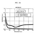
- FIGS. 5A and 5B are graphs of measured light absorbance and light transmittance respectively with respect to first electrode layer/third electrode layer (Ag/Ni) that includes a reflective electrode according to the present invention.
- the first electrode layer (Ag) and the third electrode layer (Ni) are formed in a thickness of 5 nm, respectively.
- the graphs also include the light transmittance and light absorbance of a conventional electrode layer (Ni/Au).
- the light absorbance of the Ag/Ni electrode layer is remarkably lower than that of the conventional Ni/Au electrode layer at a wavelength range of 400-800 nm.
- the light transmittance of the Ag/Ni electrode layer at the wavelength of 400 nm is more than 90 % which is greater than the light transmittance, i.e., less than 80 %, of the conventional Ni/Au electrode layer.
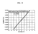
- FIG. 6 is a graph of measured current-voltage characteristic with respect to a reflective electrode (Ag/Ni-Zn alloy/Ag) according to the first embodiment of the present invention.
- the reflective electrode of the first embodiment includes first electrode layer formed of Ag, the third electrode layer formed of Ni-Zn alloy, and the fourth electrode layer formed of Ag sequentially formed on the substrate.
- Each of the first electrode layer, the third electrode layer, and the fourth electrode layer has a thickness of 2 nm, 4 nm, and 250 nm, respectively.
- Two reflective electrodes separated from each other with a distance of 4 nm were formed on the substrate, and the current-voltage characteristics between the two electrodes were measured.
- An annealing process was performed during manufacturing the reflective electrode (Ag/Ni-Zn alloy/Ag). The annealing process was performed after forming the first electrode layer and the third electrode layer at the presence of air for one minute, and another annealing process was performed after forming the fourth electrode layer at the same conditions.
- a surface of a precursor (a specimen) in which a p-type compound semiconductor layer formed of GaN as the main component is formed on a substrate is washed with trichloroethylene, acetone, methanol, and distilled water in an ultrasonic bath at 60 °C for 5 minutes each. Then, the precursor was hard baked for 10 minutes at 100 °C to remove remained moisture.
- a photoresist was spin coated on the p-type compound semiconductor layer at 4500 rpm.
- the specimen was soft baked at 85 °C for 15 minutes. After aligning a mask with the specimen, the specimen was exposed to an ultraviolet ray with an intensity of 22.8 mW for 15 second to develop a mask pattern.
- the specimen was developed by soaking in a developing solution diluted 4:1 in distilled water for approximately 25 second.
- the specimen was soaked in a BOE solution to remove a contaminant layer on the specimen.
- Ag was placed on a reaction object mounting stage in an electron-beam evaporator chamber, and a first electrode layer was deposited with Ag using the electron-beam evaporator.
- the resultant product was annealed in a rapid thermal annealing (RTA) furnace at temperature of 430-530 °C for one minute in the presence of air.
- RTA rapid thermal annealing
- a fourth electrode layer was deposited with Ag on the third electrode layer in the electron-beam evaporator.
- the resultant product on which the fourth electrode layer is formed was annealed under the same conditions as the first annealing.
- This embodiment can be applied to the method of manufacturing the light emitting device depicted in FIG. 4.
- the reflective electrode according to the present invention has low contact resistance, high reflectance, and an improved electric conductivity, thereby having a high current-voltage characteristic.
- the compound semiconductor light emitting device having the reflective electrode has low operating voltage, improved optical power, and an improved current-voltage characteristic.
- the power consumption of the compound semiconductor light emitting device is low, thereby improving light emitting efficiency of the compound semiconductor light emitting device.
- the first electrode layer according to the present invention can be applied to a light emitting diode (LED) or a laser diode (LD).
- LED light emitting diode
- LD laser diode
Landscapes
- Physics & Mathematics (AREA)
- Optics & Photonics (AREA)
- Engineering & Computer Science (AREA)
- Nanotechnology (AREA)
- Chemical & Material Sciences (AREA)
- Condensed Matter Physics & Semiconductors (AREA)
- General Physics & Mathematics (AREA)
- Electromagnetism (AREA)
- Biophysics (AREA)
- Crystallography & Structural Chemistry (AREA)
- Life Sciences & Earth Sciences (AREA)
- Geometry (AREA)
- Led Devices (AREA)
- Electrodes Of Semiconductors (AREA)
Applications Claiming Priority (1)
| Application Number | Priority Date | Filing Date | Title |
|---|---|---|---|
| KR1020040079963A KR100773538B1 (ko) | 2004-10-07 | 2004-10-07 | 반사 전극 및 이를 구비하는 화합물 반도체 발광소자 |
Publications (2)
| Publication Number | Publication Date |
|---|---|
| EP1646093A2 true EP1646093A2 (de) | 2006-04-12 |
| EP1646093A3 EP1646093A3 (de) | 2008-10-22 |
Family
ID=36179807
Family Applications (1)
| Application Number | Title | Priority Date | Filing Date |
|---|---|---|---|
| EP05253838A Withdrawn EP1646093A3 (de) | 2004-10-07 | 2005-06-21 | Reflektierende Elektrode sowie lichtemittierenden Diode aus einem Verbindungshalbleiter damit |
Country Status (5)
| Country | Link |
|---|---|
| US (1) | US7973325B2 (de) |
| EP (1) | EP1646093A3 (de) |
| JP (1) | JP2006108683A (de) |
| KR (1) | KR100773538B1 (de) |
| CN (1) | CN1758455A (de) |
Cited By (1)
| Publication number | Priority date | Publication date | Assignee | Title |
|---|---|---|---|---|
| WO2009122371A1 (en) * | 2008-04-04 | 2009-10-08 | Philips Lumileds Lighting Company, Llc | Reflective contact for a semiconductor light emitting device |
Families Citing this family (26)
| Publication number | Priority date | Publication date | Assignee | Title |
|---|---|---|---|---|
| KR100624416B1 (ko) * | 2003-12-23 | 2006-09-18 | 삼성전자주식회사 | 플립칩형 질화물계 발광소자 및 그 제조방법 |
| US7960746B2 (en) * | 2004-01-06 | 2011-06-14 | Samsung Led Co., Ltd. | Low resistance electrode and compound semiconductor light emitting device including the same |
| KR100836494B1 (ko) | 2006-12-26 | 2008-06-09 | 엘지이노텍 주식회사 | 반도체 발광소자 |
| US7888700B2 (en) * | 2007-03-08 | 2011-02-15 | Eastman Kodak Company | Quantum dot light emitting device |
| KR101047729B1 (ko) * | 2008-07-22 | 2011-07-08 | 엘지이노텍 주식회사 | 발광 소자 패키지 및 그 제조방법 |
| KR101018197B1 (ko) * | 2008-10-22 | 2011-02-28 | 삼성엘이디 주식회사 | 반도체 발광소자 |
| JP2010109013A (ja) * | 2008-10-28 | 2010-05-13 | Sanyo Electric Co Ltd | 半導体レーザ素子およびその製造方法 |
| KR101139142B1 (ko) * | 2008-11-06 | 2012-04-26 | 파나소닉 주식회사 | 질화물계 반도체 소자 및 그 제조 방법 |
| KR101068864B1 (ko) | 2008-12-03 | 2011-09-30 | 삼성엘이디 주식회사 | 반도체 발광소자 및 그 제조방법 |
| WO2010113237A1 (ja) * | 2009-04-03 | 2010-10-07 | パナソニック株式会社 | 窒化物系半導体素子およびその製造方法 |
| US20100327300A1 (en) | 2009-06-25 | 2010-12-30 | Koninklijke Philips Electronics N.V. | Contact for a semiconductor light emitting device |
| KR101171722B1 (ko) | 2009-12-25 | 2012-08-06 | 파나소닉 주식회사 | 질화물계 반도체 소자 및 그의 제조방법 |
| FR2957718B1 (fr) * | 2010-03-16 | 2012-04-20 | Commissariat Energie Atomique | Diode electroluminescente hybride a rendement eleve |
| US8933543B2 (en) | 2010-04-02 | 2015-01-13 | Panasonic Intellectual Property Management Co., Ltd. | Nitride semiconductor element having m-plane angled semiconductor region and electrode including Mg and Ag |
| CN102214762A (zh) * | 2010-04-06 | 2011-10-12 | 尚安品有限公司 | 发光二极管芯片及其封装结构 |
| KR101289602B1 (ko) * | 2011-04-21 | 2013-07-24 | 영남대학교 산학협력단 | 발광 다이오드 |
| EP2791983A4 (de) | 2011-12-12 | 2015-08-12 | Sensor Electronic Tech Inc | Uv-reflexionskontakt |
| US9818912B2 (en) | 2011-12-12 | 2017-11-14 | Sensor Electronic Technology, Inc. | Ultraviolet reflective contact |
| WO2013126458A1 (en) * | 2012-02-24 | 2013-08-29 | Skyworks Solutions, Inc. | Improved structures, devices and methods releated to copper interconnects for compound semiconductors |
| US9768357B2 (en) | 2013-01-09 | 2017-09-19 | Sensor Electronic Technology, Inc. | Ultraviolet reflective rough adhesive contact |
| WO2014110197A1 (en) | 2013-01-09 | 2014-07-17 | Sensor Electronic Technology, Inc. | Ultraviolet reflective rough adhesive contact |
| US10276749B2 (en) | 2013-01-09 | 2019-04-30 | Sensor Electronic Technology, Inc. | Ultraviolet reflective rough adhesive contact |
| EP2881982B1 (de) | 2013-12-05 | 2019-09-04 | IMEC vzw | Verfahren zur Herstellung CMOS-kompatibler Kontaktschichten in Halbleitervorrichtungen |
| CN104319621B (zh) * | 2014-10-29 | 2017-05-10 | 山东华光光电子股份有限公司 | 一种半导体激光器芯片欧姆接触金属电极及其制备方法 |
| JP2016174047A (ja) * | 2015-03-16 | 2016-09-29 | 株式会社東芝 | 半導体発光素子 |
| CN117448819B (zh) * | 2023-12-22 | 2024-03-19 | 墨卓生物科技(浙江)有限公司 | 一种用于芯片的金属电极及其制作方法 |
Citations (1)
| Publication number | Priority date | Publication date | Assignee | Title |
|---|---|---|---|---|
| WO2001047038A1 (en) | 1999-12-22 | 2001-06-28 | Lumileds Lighting U.S., Llc | Multi-layer highly reflective ohmic contacts for light-emitting semiconductor devices |
Family Cites Families (24)
| Publication number | Priority date | Publication date | Assignee | Title |
|---|---|---|---|---|
| JP2658009B2 (ja) * | 1991-07-23 | 1997-09-30 | 豊田合成株式会社 | 窒化ガリウム系化合物半導体発光素子 |
| JP2778349B2 (ja) | 1992-04-10 | 1998-07-23 | 日亜化学工業株式会社 | 窒化ガリウム系化合物半導体の電極 |
| JPH0645651A (ja) | 1992-05-22 | 1994-02-18 | Sanyo Electric Co Ltd | n型SiC用電極とその形成方法 |
| US5777350A (en) * | 1994-12-02 | 1998-07-07 | Nichia Chemical Industries, Ltd. | Nitride semiconductor light-emitting device |
| JP3620926B2 (ja) * | 1995-06-16 | 2005-02-16 | 豊田合成株式会社 | p伝導形3族窒化物半導体の電極及び電極形成方法及び素子 |
| JP3292044B2 (ja) | 1996-05-31 | 2002-06-17 | 豊田合成株式会社 | p伝導形3族窒化物半導体の電極パッド及びそれを有した素子及び素子の製造方法 |
| JPH114020A (ja) * | 1997-04-15 | 1999-01-06 | Toshiba Corp | 半導体発光素子及びその製造方法、並びに半導体発光装置 |
| DE69839300T2 (de) * | 1997-12-15 | 2009-04-16 | Philips Lumileds Lighting Company, LLC, San Jose | Licht-emittierende Vorrichtung |
| JP4118371B2 (ja) | 1997-12-15 | 2008-07-16 | フィリップス ルミレッズ ライティング カンパニー リミテッド ライアビリティ カンパニー | 電極に銀を有する窒化物半導体発光装置およびその製造方法ならびに半導体光電子装置 |
| JPH11220171A (ja) * | 1998-02-02 | 1999-08-10 | Toyoda Gosei Co Ltd | 窒化ガリウム系化合物半導体素子 |
| DE19921987B4 (de) * | 1998-05-13 | 2007-05-16 | Toyoda Gosei Kk | Licht-Abstrahlende Halbleitervorrichtung mit Gruppe-III-Element-Nitrid-Verbindungen |
| US6936859B1 (en) | 1998-05-13 | 2005-08-30 | Toyoda Gosei Co., Ltd. | Light-emitting semiconductor device using group III nitride compound |
| US6514782B1 (en) | 1999-12-22 | 2003-02-04 | Lumileds Lighting, U.S., Llc | Method of making a III-nitride light-emitting device with increased light generating capability |
| US6573537B1 (en) | 1999-12-22 | 2003-06-03 | Lumileds Lighting, U.S., Llc | Highly reflective ohmic contacts to III-nitride flip-chip LEDs |
| JP4024994B2 (ja) | 2000-06-30 | 2007-12-19 | 株式会社東芝 | 半導体発光素子 |
| JP2003168823A (ja) | 2001-09-18 | 2003-06-13 | Toyoda Gosei Co Ltd | Iii族窒化物系化合物半導体発光素子 |
| JP2004006498A (ja) * | 2002-05-31 | 2004-01-08 | Toyoda Gosei Co Ltd | Iii族窒化物系化合物半導体発光素子 |
| KR20040006056A (ko) * | 2002-07-09 | 2004-01-24 | 엘지이노텍 주식회사 | 발광 다이오드 및 그 플립칩 공정방법 |
| DE10244200A1 (de) * | 2002-09-23 | 2004-04-08 | Osram Opto Semiconductors Gmbh | Strahlungsemittierendes Halbleiterbauelement |
| TWI243488B (en) | 2003-02-26 | 2005-11-11 | Osram Opto Semiconductors Gmbh | Electrical contact-area for optoelectronic semiconductor-chip and its production method |
| JP4062171B2 (ja) * | 2003-05-28 | 2008-03-19 | ソニー株式会社 | 積層構造の製造方法 |
| US6969874B1 (en) * | 2003-06-12 | 2005-11-29 | Sandia Corporation | Flip-chip light emitting diode with resonant optical microcavity |
| KR100624416B1 (ko) | 2003-12-23 | 2006-09-18 | 삼성전자주식회사 | 플립칩형 질화물계 발광소자 및 그 제조방법 |
| KR100631840B1 (ko) * | 2004-06-03 | 2006-10-09 | 삼성전기주식회사 | 플립칩용 질화물 반도체 발광소자 |
-
2004
- 2004-10-07 KR KR1020040079963A patent/KR100773538B1/ko not_active Expired - Fee Related
-
2005
- 2005-06-21 EP EP05253838A patent/EP1646093A3/de not_active Withdrawn
- 2005-06-22 CN CNA2005100786405A patent/CN1758455A/zh active Pending
- 2005-06-22 US US11/157,971 patent/US7973325B2/en not_active Expired - Fee Related
- 2005-10-04 JP JP2005291769A patent/JP2006108683A/ja active Pending
Patent Citations (1)
| Publication number | Priority date | Publication date | Assignee | Title |
|---|---|---|---|---|
| WO2001047038A1 (en) | 1999-12-22 | 2001-06-28 | Lumileds Lighting U.S., Llc | Multi-layer highly reflective ohmic contacts for light-emitting semiconductor devices |
Cited By (1)
| Publication number | Priority date | Publication date | Assignee | Title |
|---|---|---|---|---|
| WO2009122371A1 (en) * | 2008-04-04 | 2009-10-08 | Philips Lumileds Lighting Company, Llc | Reflective contact for a semiconductor light emitting device |
Also Published As
| Publication number | Publication date |
|---|---|
| KR20060031079A (ko) | 2006-04-12 |
| CN1758455A (zh) | 2006-04-12 |
| KR100773538B1 (ko) | 2007-11-07 |
| US7973325B2 (en) | 2011-07-05 |
| JP2006108683A (ja) | 2006-04-20 |
| EP1646093A3 (de) | 2008-10-22 |
| US20060081867A1 (en) | 2006-04-20 |
Similar Documents
| Publication | Publication Date | Title |
|---|---|---|
| US7973325B2 (en) | Reflective electrode and compound semiconductor light emitting device including the same | |
| US7491979B2 (en) | Reflective electrode and compound semiconductor light emitting device including the same | |
| US7180094B2 (en) | Nitride-based light emitting device and method of manufacturing the same | |
| EP1810351B1 (de) | Gan-halbleiter-verbundleuchtelement | |
| US7541207B2 (en) | Light emitting device and method of manufacturing the same | |
| KR100682870B1 (ko) | 다층전극 및 이를 구비하는 화합물 반도체 발광소자 | |
| KR20050022242A (ko) | 질화물계 발광소자 및 그 제조방법 | |
| JP5130436B2 (ja) | GaN系半導体発光素子及びその製造方法 | |
| US7095042B2 (en) | Electrode structure, semiconductor light-emitting device having the same and method of manufacturing the same | |
| KR100764458B1 (ko) | 전극층, 이를 구비하는 발광소자 및 전극층 제조방법 |
Legal Events
| Date | Code | Title | Description |
|---|---|---|---|
| PUAI | Public reference made under article 153(3) epc to a published international application that has entered the european phase |
Free format text: ORIGINAL CODE: 0009012 |
|
| 17P | Request for examination filed |
Effective date: 20050629 |
|
| AK | Designated contracting states |
Kind code of ref document: A2 Designated state(s): AT BE BG CH CY CZ DE DK EE ES FI FR GB GR HU IE IS IT LI LT LU MC NL PL PT RO SE SI SK TR |
|
| AX | Request for extension of the european patent |
Extension state: AL BA HR LV MK YU |
|
| PUAL | Search report despatched |
Free format text: ORIGINAL CODE: 0009013 |
|
| AK | Designated contracting states |
Kind code of ref document: A3 Designated state(s): AT BE BG CH CY CZ DE DK EE ES FI FR GB GR HU IE IS IT LI LT LU MC NL PL PT RO SE SI SK TR |
|
| AX | Request for extension of the european patent |
Extension state: AL BA HR LV MK YU |
|
| AKX | Designation fees paid | ||
| REG | Reference to a national code |
Ref country code: DE Ref legal event code: 8566 |
|
| STAA | Information on the status of an ep patent application or granted ep patent |
Free format text: STATUS: THE APPLICATION IS DEEMED TO BE WITHDRAWN |
|
| 18D | Application deemed to be withdrawn |
Effective date: 20090423 |