EP1648207A2 - Kapazitive/Resistive Vorrichtungen, organische dielektrische Laminate hoher Dielektrizitätskonstante und Leiterplatten mit solchen Vorrichtungen, und Verfahren zu deren Herstellung - Google Patents
Kapazitive/Resistive Vorrichtungen, organische dielektrische Laminate hoher Dielektrizitätskonstante und Leiterplatten mit solchen Vorrichtungen, und Verfahren zu deren Herstellung Download PDFInfo
- Publication number
- EP1648207A2 EP1648207A2 EP05020896A EP05020896A EP1648207A2 EP 1648207 A2 EP1648207 A2 EP 1648207A2 EP 05020896 A EP05020896 A EP 05020896A EP 05020896 A EP05020896 A EP 05020896A EP 1648207 A2 EP1648207 A2 EP 1648207A2
- Authority
- EP
- European Patent Office
- Prior art keywords
- dielectric
- capacitive
- electrode
- resistive device
- resistor element
- Prior art date
- Legal status (The legal status is an assumption and is not a legal conclusion. Google has not performed a legal analysis and makes no representation as to the accuracy of the status listed.)
- Granted
Links
Images


Classifications
-
- H—ELECTRICITY
- H01—ELECTRIC ELEMENTS
- H01C—RESISTORS
- H01C17/00—Apparatus or processes specially adapted for manufacturing resistors
- H01C17/06—Apparatus or processes specially adapted for manufacturing resistors adapted for coating resistive material on a base
- H01C17/065—Apparatus or processes specially adapted for manufacturing resistors adapted for coating resistive material on a base by thick film techniques, e.g. serigraphy
- H01C17/06506—Precursor compositions therefor, e.g. pastes, inks, glass frits or green body
- H01C17/06513—Precursor compositions therefor, e.g. pastes, inks, glass frits or green body characterised by the resistive component
- H01C17/06533—Precursor compositions therefor, e.g. pastes, inks, glass frits or green body characterised by the resistive component composed of oxides
-
- H—ELECTRICITY
- H05—ELECTRIC TECHNIQUES NOT OTHERWISE PROVIDED FOR
- H05K—PRINTED CIRCUITS; CASINGS OR CONSTRUCTIONAL DETAILS OF ELECTRIC APPARATUS; MANUFACTURE OF ASSEMBLAGES OF ELECTRICAL COMPONENTS
- H05K1/00—Printed circuits
- H05K1/16—Printed circuits incorporating printed electric components, e.g. printed resistors, capacitors or inductors
-
- H—ELECTRICITY
- H01—ELECTRIC ELEMENTS
- H01C—RESISTORS
- H01C17/00—Apparatus or processes specially adapted for manufacturing resistors
- H01C17/06—Apparatus or processes specially adapted for manufacturing resistors adapted for coating resistive material on a base
- H01C17/065—Apparatus or processes specially adapted for manufacturing resistors adapted for coating resistive material on a base by thick film techniques, e.g. serigraphy
- H01C17/06506—Precursor compositions therefor, e.g. pastes, inks, glass frits or green body
- H01C17/06573—Precursor compositions therefor, e.g. pastes, inks, glass frits or green body characterised by the permanent binder
- H01C17/06586—Precursor compositions therefor, e.g. pastes, inks, glass frits or green body characterised by the permanent binder composed of organic material
-
- H—ELECTRICITY
- H01—ELECTRIC ELEMENTS
- H01C—RESISTORS
- H01C7/00—Non-adjustable resistors formed as one or more layers or coatings; Non-adjustable resistors made from powdered conducting material or powdered semi-conducting material with or without insulating material
- H01C7/003—Thick film resistors
- H01C7/005—Polymer thick films
-
- H—ELECTRICITY
- H01—ELECTRIC ELEMENTS
- H01G—CAPACITORS; CAPACITORS, RECTIFIERS, DETECTORS, SWITCHING DEVICES, LIGHT-SENSITIVE OR TEMPERATURE-SENSITIVE DEVICES OF THE ELECTROLYTIC TYPE
- H01G4/00—Fixed capacitors; Processes of their manufacture
- H01G4/40—Structural combinations of fixed capacitors with other electric elements, the structure mainly consisting of a capacitor, e.g. RC combinations
-
- H—ELECTRICITY
- H05—ELECTRIC TECHNIQUES NOT OTHERWISE PROVIDED FOR
- H05K—PRINTED CIRCUITS; CASINGS OR CONSTRUCTIONAL DETAILS OF ELECTRIC APPARATUS; MANUFACTURE OF ASSEMBLAGES OF ELECTRICAL COMPONENTS
- H05K1/00—Printed circuits
- H05K1/16—Printed circuits incorporating printed electric components, e.g. printed resistors, capacitors or inductors
- H05K1/162—Printed circuits incorporating printed electric components, e.g. printed resistors, capacitors or inductors incorporating printed capacitors
-
- H—ELECTRICITY
- H05—ELECTRIC TECHNIQUES NOT OTHERWISE PROVIDED FOR
- H05K—PRINTED CIRCUITS; CASINGS OR CONSTRUCTIONAL DETAILS OF ELECTRIC APPARATUS; MANUFACTURE OF ASSEMBLAGES OF ELECTRICAL COMPONENTS
- H05K1/00—Printed circuits
- H05K1/16—Printed circuits incorporating printed electric components, e.g. printed resistors, capacitors or inductors
- H05K1/167—Printed circuits incorporating printed electric components, e.g. printed resistors, capacitors or inductors incorporating printed resistors
-
- H—ELECTRICITY
- H05—ELECTRIC TECHNIQUES NOT OTHERWISE PROVIDED FOR
- H05K—PRINTED CIRCUITS; CASINGS OR CONSTRUCTIONAL DETAILS OF ELECTRIC APPARATUS; MANUFACTURE OF ASSEMBLAGES OF ELECTRICAL COMPONENTS
- H05K2201/00—Indexing scheme relating to printed circuits covered by H05K1/00
- H05K2201/02—Fillers; Particles; Fibers; Reinforcement materials
- H05K2201/0203—Fillers and particles
- H05K2201/0206—Materials
- H05K2201/0209—Inorganic, non-metallic particles
-
- H—ELECTRICITY
- H05—ELECTRIC TECHNIQUES NOT OTHERWISE PROVIDED FOR
- H05K—PRINTED CIRCUITS; CASINGS OR CONSTRUCTIONAL DETAILS OF ELECTRIC APPARATUS; MANUFACTURE OF ASSEMBLAGES OF ELECTRICAL COMPONENTS
- H05K2201/00—Indexing scheme relating to printed circuits covered by H05K1/00
- H05K2201/09—Shape and layout
- H05K2201/09209—Shape and layout details of conductors
- H05K2201/0929—Conductive planes
- H05K2201/09309—Core having two or more power planes; Capacitive laminate of two power planes
-
- H—ELECTRICITY
- H05—ELECTRIC TECHNIQUES NOT OTHERWISE PROVIDED FOR
- H05K—PRINTED CIRCUITS; CASINGS OR CONSTRUCTIONAL DETAILS OF ELECTRIC APPARATUS; MANUFACTURE OF ASSEMBLAGES OF ELECTRICAL COMPONENTS
- H05K2201/00—Indexing scheme relating to printed circuits covered by H05K1/00
- H05K2201/09—Shape and layout
- H05K2201/09209—Shape and layout details of conductors
- H05K2201/09654—Shape and layout details of conductors covering at least two types of conductors provided for in H05K2201/09218 - H05K2201/095
- H05K2201/09763—Printed component having superposed conductors, but integrated in one circuit layer
-
- H—ELECTRICITY
- H05—ELECTRIC TECHNIQUES NOT OTHERWISE PROVIDED FOR
- H05K—PRINTED CIRCUITS; CASINGS OR CONSTRUCTIONAL DETAILS OF ELECTRIC APPARATUS; MANUFACTURE OF ASSEMBLAGES OF ELECTRICAL COMPONENTS
- H05K3/00—Apparatus or processes for manufacturing printed circuits
- H05K3/40—Forming printed elements for providing electric connections to or between printed circuits
- H05K3/42—Plated through-holes or plated via connections
- H05K3/429—Plated through-holes specially for multilayer circuits, e.g. having connections to inner circuit layers
-
- Y—GENERAL TAGGING OF NEW TECHNOLOGICAL DEVELOPMENTS; GENERAL TAGGING OF CROSS-SECTIONAL TECHNOLOGIES SPANNING OVER SEVERAL SECTIONS OF THE IPC; TECHNICAL SUBJECTS COVERED BY FORMER USPC CROSS-REFERENCE ART COLLECTIONS [XRACs] AND DIGESTS
- Y10—TECHNICAL SUBJECTS COVERED BY FORMER USPC
- Y10T—TECHNICAL SUBJECTS COVERED BY FORMER US CLASSIFICATION
- Y10T29/00—Metal working
- Y10T29/49—Method of mechanical manufacture
- Y10T29/49002—Electrical device making
- Y10T29/49117—Conductor or circuit manufacturing
- Y10T29/49124—On flat or curved insulated base, e.g., printed circuit, etc.
- Y10T29/49155—Manufacturing circuit on or in base
Definitions
- Capacitors and resistors may be used in series for transmission line termination of signal traces extending between integrated circuit (IC) devices.
- the capacitors and resistors are used to match the impedance of an IC device to a line, or to reduce or eliminate signal reflection.
- Some circuits are continuous load and use a resistor in parallel with the line.
- Non-continuous load circuits have a resistor and capacitor in series and are useful for low power lcs.
- FIG. 1 schematically illustrates a non-continuous load termination of IC devices 10 and 20 known in the prior art.
- the distance from a to b is typically short.
- the value of the resistor R is chosen to match the line impedance and is typically about 45-80 ohms.
- the value of the capacitor C is chosen so that the RC time constant of the resistor R and the capacitor C in series is greater than the rise time of a signal and less than the total time of the signal pulse. Typical capacitance values are on the order of 30 picoFarads.
- FIG. 2 is a cross section view of a portion of a printed circuit board 25 having a SMT resistor 40 and a SMT capacitor 50 connected to an IC device 30 to form a conventional SMT RC transmission line termination for the IC 30.
- the signal line carrying the signal to the IC 30 is connected to a circuit trace 60 connecting the IC device 30 to the resistor 40.
- the capacitor 50 is coupled to a circuit trace 70 by one of a pair of solder pads 52 and solder joints 58.
- the resistor 40 is coupled to the circuit trace 70 by a solder pad 42 and a solder joint 48.
- the capacitor 50 is coupled to a via hole 80 by the other solder pad 58 and a circuit trace 59.
- This arrangement places the resistor 40 and the capacitor 50 in series with the signal line and connected to ground through a plated through-hole via 80.
- This conventional surface mount approach requires use of valuable surface real estate. Further, the requirement for solder joints reduces reliability and increases costs of fabrication.
- a capacitive/resistive device comprises a first electrode, a dielectric disposed over the first electrode, a resistor element disposed over a second electrode and adjacent to the dielectric wherein the dielectric comprises a polymer filled with a high dielectric constant powder phase.
- the capacitive/resistive device can be embedded in organic dielectric laminates, and incorporated in printed wiring boards.
- both the resistor and the capacitor functions may be integrated into a single buried laminate, reducing the cost and difficulty in creating the resistor and capacitor functions.
- the capacitive/resistive device is incorporated in a printed wiring board, embedding the capacitive/resistive device also frees up valuable real estate. Further, solder joints associated with SMT devices may be eliminated, thereby improving reliability.
- the capacitive/resistive device can be processed using conventional etching processes, further reducing production costs.
- FIG. 1 is a schematic illustration of a conventional (prior art) non-continuous load termination having a resistor and capacitor in series;
- FIG. 2 is a cross section view of a printed wiring board having a conventional (prior art) SMT RC transmission line termination for an integrated circuit device;
- FIG. 3 is a section view of a portion of a printed wiring board having an embedded capacitive/resistive device according to a second embodiment
- FIGS. 4A-4F illustrate a method according to the present invention of making a laminate structure including the capacitive/resistive device illustrated in FIG. 3.
- Embodiments of the present invention are addressed to capacitive/resistive devices that may be buried in the substrate of a printed wiring board (PWB). Providing the capacitive and resistive functions within the PWB substrate conserves valuable surface real estate on the printed wiring board. The embodiments of the present invention also require fewer solder joints than conventional SMT termination arrangements.
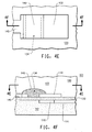
- FIG. 3 is a section view of a portion of a printed wiring board 2000.
- the printed wiring board section 2000 includes an RC transmission line termination in which the resistor function and the capacitor function are integrated into a single capacitive/resistive device 200.
- the device 200 comprises a bottom electrode 210, a dielectric 220, a resistor element 230, a top electrode or top plate 240, and a conductive trace 245.
- the device 200 provides a resistive and a capacitive function in a single laminate structure, generally indicated by the bracket 201.
- the device 200 is coupled to an IC device 270 by the conductive circuit trace 245, a plated through hole via 250 extending through a dielectric layer 280, and a conductive circuit trace 260.
- the IC device 270 may be connected to the conductive circuit trace 260 by a solder pad 272 and a solder joint 274.
- a conductive circuit trace 211 may extend from the bottom electrode 210 for connection to ground or other circuitry.
- FIGS. 4A-4F illustrate a method of making a laminate including the device 200.
- FIG. 4A is a section view in front elevation of a first stage of manufacture in which first and second metallic foils 212, 242 are provided.
- the second metallic foil 242 is provided with a layer of resistor material 232.
- the resistor material 232 can be, for example, NiP, CrSi, NiCr or other electrically resistive materials that can be plated, sputtered or otherwise deposited over the surface of the second metallic foil 242.
- the first and second metallic foils 212, 242 can be made from, for example, copper, copper-based materials, and other metals.
- a high dielectric constant slurry may be cast or coated onto the first foil 212 and cured, forming a first dielectric layer 222.
- a similar, second dielectric layer 226 may be formed in a similar manner on the second foil 242, over the surface of the layer of resistor material 232.
- Slurry materials may comprise, for example, a polymer-solvent solution with a high dielectric constant ("high K") filler or functional phase.
- high K high dielectric constant
- Suitable polymers for slurry or solution may include, for example, epoxies or polyimide resins.
- High K functional phases may be defined as materials with dielectric constants of greater than 500 and may include perovskites of the general formula ABO 3 .
- Suitable fillers include, for example, crystalline barium titanate (BT), barium strontium titanate (BST), lead zirconate titanate (PZT), lead lanthanum titanate, lead lanthanum zirconate titanate (PLZT), lead magnesium niobate (PMN), and calcium copper titanate and mixtures thereof. Fillers may be in powder form.
- a thin adhesive layer 227 may be applied to one or both surfaces of either of the dielectric layers 222, 226 (shown in FIG. 4A on the layer 222).
- the adhesive layer 227 may be formed from, for example, a thermoplastic polymer and may be filled with a high dielectric phase to avoid dilution of the dielectric constant. The two structures are then laminated together in the direction of the arrows shown in FIG. 4A.
- lamination forms a single dielectric 220 from the layers 222, 226 and 227.
- This dielectric layer may have a dielectric constant in the range of 5 to 40.
- the adhesive layer 227 facilitates joining of the dielectric layers 222 and 226 during the lamination process.
- the adhesive layer 227 may be dispensed with if the dielectric layers 222 and 226 are only partially cured prior to lamination, or, are of a thermoplastic nature so that upon lamination a suitable temperature and pressure will sufficiently soften the resin so that the layers 224 and 226 bond without adhesive.
- 4B may also be formed by casting a slurry onto only one of the foils 212, 242 and laminating the other foil to the cured or partially cured slurry. Yet another alternative method would be to form a free-standing film of the cured or partially cured slurry 220 and laminate foils 212 and 242 to both sides of the polymer film 220.
- FIG. 4C is a bottom section view of the resulting article, taken on line 4C-4C in FIG. 4D. Referring to FIG. 4C, the etching produces the bottom electrode 210 of the device 200 and the conductive circuit trace 211.
- FIG. 4D is a section view in front elevation taken on line 4D-4D in FIG. 4C.
- the bottom electrode 210 side of the resulting article is laminated to a laminate material 282.
- the lamination can be performed, for example, using FR4 prepreg, or other prepregs, in standard printing wiring board processes.
- FIG. 4E is a top section view of the resulting article, taken on line 4E-4E in FIG. 4F.
- FIG. 4F is a section view in front elevation, taken on line 4F-4F in FIG. 4E.
- the etching produces the top electrode 240 of the device 200 and the conductive circuit trace 245. Etching also produces a gap 248.
- a photoresist (not shown in FIGS. 4E and 4F) may be re-applied and the resistor material 232 may be imaged and etched using etching solutions that remove resistor material. In this way, the layer of resistor material 232 can be selectively etched to form a resistor element 230 having any desired shape and dimensions.
- the resultant resistor element 230 bridges the gap 248 and extends between the top conductor 240 and the conductive trace 245.
- a dielectric layer 280 is laminated to the component side of the dielectric layer 282, forming a laminate structure 201.
- the laminate structure 201 can then be incorporated into, for example, a printed wiring board using conventional lamination and via formation processes.
- Example 1 This example of the device 200 is discussed with reference to FIG. 3.
- the initial laminate structure shown in FIG. 4B consists of copper foil 242 plated with a resistive material 232 that is composed of a nickel phosphorus alloy of sheet resistivity 50 ohms per square.
- the dielectric 220 is a barium titanate-filled thermoplastic polyimide. Barium titanate is advantageous as a filler as it is readily available and lead-free.
- the dielectric 220 is 14 microns thick and has a dielectric constant of 11, thereby yielding a capacitance density of 4.5 nanoFarads per square inch.
- Electrodes 210 and 240 are formed from etching copper foils 212 and 242.. The above capacitor is easy to make to relatively high tolerances.
- Example 2 This example of the device 200 is discussed with reference to FIG. 3.
- the initial laminate structure shown in FIG. 4B consists of copper foil 242 plated with a resistive material 232 that is composed of a nickel phosphorus alloy of sheet resistivity 50 ohms per square.
- the dielectric 220 is a barium titanate-filled thermoplastic polyimide. Barium titanate is advantageous as a filler as it is readily available and lead-free.
- the dielectric 220 is 8 microns thick and has a dielectric constant of 11, thereby yielding a capacitance density of 6.2 nanoFarads per square inch.
- Electrodes 210 and 240 are formed from etching copper foils 212 and 242. The above capacitor is easy to make to relatively high tolerances.
- thin high dielectric constant capacitor laminate structures in combination with resistors may be used to reduce the size of the buried capacitor function and to more effectively bury RC transmission line terminations. Embedding the capacitor and resistor functions frees up valuable board surface real estate and eliminates solder joints associated with SMT devices, thereby improving reliability. Further, the laminates combining resistance and capacitance within the laminate can be processed using conventional etching processes, which reduces production costs.
- one piece of laminate can be used to embed many discrete resistors and many discrete capacitors, which reduces the inductance associated with connecting resistors and capacitors.
- the shapes of the capacitor embodiments in top plan view are generally rectangular.
- the capacitor electrodes, dielectrics, and other components and layers can have other regular or irregular surface area shapes, such as, for example, round, oblong, oval or polygonal shapes.
- a single capacitive/resistive device 200 is formed in each of the laminate structures 201 described above.
- panel structures and printed wiring boards can include a large number of individual capacitive/resistive devices of differing type and arrangement.
- resistance, capacitance and inductance combine to create a specific circuit impedance, typically identified by the capital letter Z.
- the resistance and capacitance may be structured to achieve a specific impedance. Changing the resistance, capacitance, or both will change the inductance. All three changes can be controlled to define the final impedance. In other words, the impedance of the laminate is 'tunable.'
Landscapes
- Engineering & Computer Science (AREA)
- Microelectronics & Electronic Packaging (AREA)
- Power Engineering (AREA)
- Manufacturing & Machinery (AREA)
- Physics & Mathematics (AREA)
- Electromagnetism (AREA)
- Production Of Multi-Layered Print Wiring Board (AREA)
- Parts Printed On Printed Circuit Boards (AREA)
- Fixed Capacitors And Capacitor Manufacturing Machines (AREA)
Applications Claiming Priority (1)
| Application Number | Priority Date | Filing Date | Title |
|---|---|---|---|
| US10/967,781 US7382627B2 (en) | 2004-10-18 | 2004-10-18 | Capacitive/resistive devices, organic dielectric laminates and printed wiring boards incorporating such devices, and methods of making thereof |
Publications (3)
| Publication Number | Publication Date |
|---|---|
| EP1648207A2 true EP1648207A2 (de) | 2006-04-19 |
| EP1648207A3 EP1648207A3 (de) | 2008-02-20 |
| EP1648207B1 EP1648207B1 (de) | 2012-05-02 |
Family
ID=35730635
Family Applications (1)
| Application Number | Title | Priority Date | Filing Date |
|---|---|---|---|
| EP05020896A Ceased EP1648207B1 (de) | 2004-10-18 | 2005-09-26 | Kapazitive/Resistive Vorrichtungen, organische dielektrische Laminate hoher Dielektrizitätskonstante und Leiterplatten mit solchen Vorrichtungen, und Verfahren zu deren Herstellung |
Country Status (6)
| Country | Link |
|---|---|
| US (1) | US7382627B2 (de) |
| EP (1) | EP1648207B1 (de) |
| JP (1) | JP4500759B2 (de) |
| KR (1) | KR100729703B1 (de) |
| CN (1) | CN1783377A (de) |
| TW (1) | TWI397354B (de) |
Families Citing this family (13)
| Publication number | Priority date | Publication date | Assignee | Title |
|---|---|---|---|---|
| US7596842B2 (en) * | 2005-02-22 | 2009-10-06 | Oak-Mitsui Inc. | Method of making multilayered construction for use in resistors and capacitors |
| US20060286696A1 (en) * | 2005-06-21 | 2006-12-21 | Peiffer Joel S | Passive electrical article |
| CN101090599B (zh) * | 2006-06-16 | 2010-05-26 | 鸿富锦精密工业(深圳)有限公司 | 电路板 |
| US7808797B2 (en) * | 2006-12-11 | 2010-10-05 | Intel Corporation | Microelectronic substrate including embedded components and spacer layer and method of forming same |
| DE602007006238D1 (de) | 2006-12-21 | 2010-06-10 | Cardiac Pacemakers Inc | Festkörper-impulstherapiekondensator |
| US7672113B2 (en) * | 2007-09-14 | 2010-03-02 | Oak-Mitsui, Inc. | Polymer-ceramic composites with excellent TCC |
| US8957531B2 (en) * | 2011-10-20 | 2015-02-17 | International Business Machines Corporation | Flat laminate, symmetrical test structures and method of use to gauge white bump sensitivity |
| CN105047642B (zh) * | 2015-08-12 | 2024-01-19 | 深圳市槟城电子股份有限公司 | 一种端口防护电路集成封装件 |
| CN105047411A (zh) * | 2015-08-12 | 2015-11-11 | 深圳市槟城电子有限公司 | 一种电阻和电容串连的组件及其制作方法 |
| US10083781B2 (en) | 2015-10-30 | 2018-09-25 | Vishay Dale Electronics, Llc | Surface mount resistors and methods of manufacturing same |
| US10438729B2 (en) | 2017-11-10 | 2019-10-08 | Vishay Dale Electronics, Llc | Resistor with upper surface heat dissipation |
| JP7438901B2 (ja) * | 2020-09-11 | 2024-02-27 | キオクシア株式会社 | スイッチング回路および記憶装置 |
| CN117457395A (zh) | 2022-07-19 | 2024-01-26 | 国巨电子(中国)有限公司 | 薄膜晶片电阻电容及其制作方法 |
Family Cites Families (36)
| Publication number | Priority date | Publication date | Assignee | Title |
|---|---|---|---|---|
| US3934119A (en) * | 1974-09-17 | 1976-01-20 | Texas Instruments Incorporated | Electrical resistance heaters |
| US4377652A (en) * | 1978-02-17 | 1983-03-22 | Asahi Kasei Kogyo Kabushiki Kaisha | Polyamide-imide compositions and articles for electrical use prepared therefrom |
| US4410867A (en) * | 1978-12-28 | 1983-10-18 | Western Electric Company, Inc. | Alpha tantalum thin film circuit device |
| US4399417A (en) * | 1980-06-06 | 1983-08-16 | Bell Telephone Laboratories, Incorporated | Integrated CRC filter circuit |
| US4407883A (en) * | 1982-03-03 | 1983-10-04 | Uop Inc. | Laminates for printed circuit boards |
| JPS58190091A (ja) * | 1982-04-30 | 1983-11-05 | 宇部興産株式会社 | フレキシブル配線基板の製造方法 |
| JPS60113993A (ja) * | 1983-11-25 | 1985-06-20 | 三菱電機株式会社 | 多層回路基板の製造方法 |
| US5093036A (en) * | 1988-09-20 | 1992-03-03 | Raychem Corporation | Conductive polymer composition |
| JP3019541B2 (ja) * | 1990-11-22 | 2000-03-13 | 株式会社村田製作所 | コンデンサ内蔵型配線基板およびその製造方法 |
| JPH0548271A (ja) * | 1991-08-12 | 1993-02-26 | Murata Mfg Co Ltd | 機能性多層回路基板 |
| JPH0565456A (ja) * | 1991-09-09 | 1993-03-19 | Sumitomo Bakelite Co Ltd | 気密封止用樹脂ペースト |
| JPH05152111A (ja) * | 1991-11-28 | 1993-06-18 | Rohm Co Ltd | チツプ型複合部品 |
| DE69305942T2 (de) * | 1992-09-15 | 1997-03-13 | Du Pont | Zusammensetzung für einen Polymer-Dickschichtwiderstand |
| US6111005A (en) * | 1993-07-30 | 2000-08-29 | Diemat, Inc. | Polymeric adhesive paste |
| US6140402A (en) * | 1993-07-30 | 2000-10-31 | Diemat, Inc. | Polymeric adhesive paste |
| JP3117175B2 (ja) | 1994-02-09 | 2000-12-11 | アルプス電気株式会社 | 抵抗体 |
| TW301843B (en) * | 1994-11-15 | 1997-04-01 | Ibm | Electrically conductive paste and composite and their use as an electrically conductive connector |
| TW367621B (en) * | 1995-02-27 | 1999-08-21 | Nxp Bv | Electronic component comprising a thin-film structure with passive elements |
| JPH08306503A (ja) * | 1995-05-11 | 1996-11-22 | Rohm Co Ltd | チップ状電子部品 |
| JPH0992983A (ja) * | 1995-07-17 | 1997-04-04 | Sumitomo Kinzoku Electro Device:Kk | セラミック多層基板の製造方法 |
| US5699224A (en) * | 1995-10-25 | 1997-12-16 | Rohm Co., Ltd. | Thick-film capacitor and chip-type composite electronic component utilizing the same |
| JPH09186004A (ja) * | 1995-12-28 | 1997-07-15 | Kyocera Corp | C−r複合電子部品 |
| EP0902048B1 (de) * | 1997-09-11 | 2005-11-23 | E.I. Du Pont De Nemours And Company | Flexible Polyimidfolie mit hoher dielektrischer Konstante |
| US5993698A (en) | 1997-11-06 | 1999-11-30 | Acheson Industries, Inc. | Electrical device containing positive temperature coefficient resistor composition and method of manufacturing the device |
| KR19990071099A (ko) * | 1998-02-27 | 1999-09-15 | 윤종용 | 인쇄회로기판 및 그 제조방법 |
| JP4297617B2 (ja) * | 1999-03-17 | 2009-07-15 | モトローラ・インコーポレイテッド | 抵抗器を製作する方法 |
| US6030553A (en) * | 1999-04-01 | 2000-02-29 | Industrial Technology Research Institute | Polymer thick film resistor pastes |
| US6535398B1 (en) * | 2000-03-07 | 2003-03-18 | Fujitsu Limited | Multichip module substrates with buried discrete capacitors and components and methods for making |
| US6278356B1 (en) * | 2000-05-17 | 2001-08-21 | Compeq Manufacturing Company Limited | Flat, built-in resistors and capacitors for a printed circuit board |
| US6541137B1 (en) * | 2000-07-31 | 2003-04-01 | Motorola, Inc. | Multi-layer conductor-dielectric oxide structure |
| US6657849B1 (en) * | 2000-08-24 | 2003-12-02 | Oak-Mitsui, Inc. | Formation of an embedded capacitor plane using a thin dielectric |
| TW511405B (en) * | 2000-12-27 | 2002-11-21 | Matsushita Electric Industrial Co Ltd | Device built-in module and manufacturing method thereof |
| US7524528B2 (en) * | 2001-10-05 | 2009-04-28 | Cabot Corporation | Precursor compositions and methods for the deposition of passive electrical components on a substrate |
| KR100455891B1 (ko) * | 2002-12-24 | 2004-11-06 | 삼성전기주식회사 | 커패시터 내장형 인쇄회로기판 및 그 제조 방법 |
| US6910264B2 (en) * | 2003-01-03 | 2005-06-28 | Phoenix Precision Technology Corp. | Method for making a multilayer circuit board having embedded passive components |
| JP4449772B2 (ja) * | 2004-04-09 | 2010-04-14 | 株式会社デンソー | パワー半導体スイッチング素子及びそれを用いた半導体パワーモジュール |
-
2004
- 2004-10-18 US US10/967,781 patent/US7382627B2/en not_active Expired - Lifetime
-
2005
- 2005-09-26 EP EP05020896A patent/EP1648207B1/de not_active Ceased
- 2005-10-04 TW TW094134608A patent/TWI397354B/zh not_active IP Right Cessation
- 2005-10-17 KR KR1020050097353A patent/KR100729703B1/ko not_active Expired - Fee Related
- 2005-10-18 JP JP2005303551A patent/JP4500759B2/ja not_active Expired - Fee Related
- 2005-10-18 CN CNA2005101161069A patent/CN1783377A/zh active Pending
Also Published As
| Publication number | Publication date |
|---|---|
| US7382627B2 (en) | 2008-06-03 |
| CN1783377A (zh) | 2006-06-07 |
| JP2006121087A (ja) | 2006-05-11 |
| TW200628025A (en) | 2006-08-01 |
| KR100729703B1 (ko) | 2007-06-19 |
| US20060082982A1 (en) | 2006-04-20 |
| TWI397354B (zh) | 2013-05-21 |
| EP1648207A3 (de) | 2008-02-20 |
| KR20060054032A (ko) | 2006-05-22 |
| EP1648207B1 (de) | 2012-05-02 |
| JP4500759B2 (ja) | 2010-07-14 |
Similar Documents
| Publication | Publication Date | Title |
|---|---|---|
| EP1648208B1 (de) | Kapazitive/Resistive Einrichtungen und Leiterplatten mit solchen Einrichtungen sowie Herstellungsverfahren dafür | |
| US7813141B2 (en) | Capacitive/resistive devices, organic dielectric laminates and printed wiring boards incorporating such devices, and methods of making thereof | |
| EP1648207B1 (de) | Kapazitive/Resistive Vorrichtungen, organische dielektrische Laminate hoher Dielektrizitätskonstante und Leiterplatten mit solchen Vorrichtungen, und Verfahren zu deren Herstellung | |
| EP1675131B1 (de) | Kondensatorvorrichtungen, organische dielektrische Laminate und Leiterplatten enthaltend solche Vorrichtungen, sowie Verfahren zu deren Herstellung | |
| KR101401863B1 (ko) | 커패시터 내장형 인쇄회로기판 및 그 제조방법 | |
| EP1720393A3 (de) | Mehrschichtige Leiterplatte und ihre Herstellung | |
| KR20060071334A (ko) | 전력 코어 장치 및 그 제조 방법 | |
| EP1675449A1 (de) | Vorrichtungen mit Stromverteilungskern und Herstellungsverfahren dafür | |
| JP4207517B2 (ja) | 素子内蔵基板 | |
| JP4269657B2 (ja) | 誘電体積層シート、基板内蔵キャパシターシート及び素子内蔵基板 | |
| JPH1056251A (ja) | 電子部品内蔵プリント基板およびその製造方法 | |
| JP4684483B2 (ja) | 多層回路基板の製造方法 |
Legal Events
| Date | Code | Title | Description |
|---|---|---|---|
| PUAI | Public reference made under article 153(3) epc to a published international application that has entered the european phase |
Free format text: ORIGINAL CODE: 0009012 |
|
| AK | Designated contracting states |
Kind code of ref document: A2 Designated state(s): AT BE BG CH CY CZ DE DK EE ES FI FR GB GR HU IE IS IT LI LT LU LV MC NL PL PT RO SE SI SK TR |
|
| AX | Request for extension of the european patent |
Extension state: AL BA HR MK YU |
|
| PUAL | Search report despatched |
Free format text: ORIGINAL CODE: 0009013 |
|
| AK | Designated contracting states |
Kind code of ref document: A3 Designated state(s): AT BE BG CH CY CZ DE DK EE ES FI FR GB GR HU IE IS IT LI LT LU LV MC NL PL PT RO SE SI SK TR |
|
| AX | Request for extension of the european patent |
Extension state: AL BA HR MK YU |
|
| 17P | Request for examination filed |
Effective date: 20080702 |
|
| 17Q | First examination report despatched |
Effective date: 20080811 |
|
| AKX | Designation fees paid |
Designated state(s): DE FR GB |
|
| GRAP | Despatch of communication of intention to grant a patent |
Free format text: ORIGINAL CODE: EPIDOSNIGR1 |
|
| GRAS | Grant fee paid |
Free format text: ORIGINAL CODE: EPIDOSNIGR3 |
|
| GRAA | (expected) grant |
Free format text: ORIGINAL CODE: 0009210 |
|
| RAP1 | Party data changed (applicant data changed or rights of an application transferred) |
Owner name: CDA PROCESSING LIMITED LIABILITY COMPANY |
|
| AK | Designated contracting states |
Kind code of ref document: B1 Designated state(s): DE FR GB |
|
| REG | Reference to a national code |
Ref country code: GB Ref legal event code: FG4D |
|
| REG | Reference to a national code |
Ref country code: DE Ref legal event code: R096 Ref document number: 602005033952 Country of ref document: DE Effective date: 20120712 |
|
| PLBE | No opposition filed within time limit |
Free format text: ORIGINAL CODE: 0009261 |
|
| STAA | Information on the status of an ep patent application or granted ep patent |
Free format text: STATUS: NO OPPOSITION FILED WITHIN TIME LIMIT |
|
| 26N | No opposition filed |
Effective date: 20130205 |
|
| REG | Reference to a national code |
Ref country code: DE Ref legal event code: R097 Ref document number: 602005033952 Country of ref document: DE Effective date: 20130205 |
|
| REG | Reference to a national code |
Ref country code: FR Ref legal event code: PLFP Year of fee payment: 12 |
|
| REG | Reference to a national code |
Ref country code: FR Ref legal event code: PLFP Year of fee payment: 13 |
|
| REG | Reference to a national code |
Ref country code: FR Ref legal event code: PLFP Year of fee payment: 14 |
|
| P01 | Opt-out of the competence of the unified patent court (upc) registered |
Effective date: 20230527 |
|
| PGFP | Annual fee paid to national office [announced via postgrant information from national office to epo] |
Ref country code: GB Payment date: 20230810 Year of fee payment: 19 |
|
| PGFP | Annual fee paid to national office [announced via postgrant information from national office to epo] |
Ref country code: FR Payment date: 20230807 Year of fee payment: 19 Ref country code: DE Payment date: 20230808 Year of fee payment: 19 |
|
| REG | Reference to a national code |
Ref country code: DE Ref legal event code: R119 Ref document number: 602005033952 Country of ref document: DE |
|
| GBPC | Gb: european patent ceased through non-payment of renewal fee |
Effective date: 20240926 |
|
| PG25 | Lapsed in a contracting state [announced via postgrant information from national office to epo] |
Ref country code: DE Free format text: LAPSE BECAUSE OF NON-PAYMENT OF DUE FEES Effective date: 20250401 |
|
| PG25 | Lapsed in a contracting state [announced via postgrant information from national office to epo] |
Ref country code: GB Free format text: LAPSE BECAUSE OF NON-PAYMENT OF DUE FEES Effective date: 20240926 |
|
| PG25 | Lapsed in a contracting state [announced via postgrant information from national office to epo] |
Ref country code: FR Free format text: LAPSE BECAUSE OF NON-PAYMENT OF DUE FEES Effective date: 20240930 |