EP1659622A2 - Feldeffekttransistor und Verfahren zu seiner Herstellung - Google Patents
Feldeffekttransistor und Verfahren zu seiner Herstellung Download PDFInfo
- Publication number
- EP1659622A2 EP1659622A2 EP05292446A EP05292446A EP1659622A2 EP 1659622 A2 EP1659622 A2 EP 1659622A2 EP 05292446 A EP05292446 A EP 05292446A EP 05292446 A EP05292446 A EP 05292446A EP 1659622 A2 EP1659622 A2 EP 1659622A2
- Authority
- EP
- European Patent Office
- Prior art keywords
- electrode
- effect transistor
- field effect
- layer
- semiconductor layer
- Prior art date
- Legal status (The legal status is an assumption and is not a legal conclusion. Google has not performed a legal analysis and makes no representation as to the accuracy of the status listed.)
- Granted
Links
Images


Classifications
-
- H—ELECTRICITY
- H10—SEMICONDUCTOR DEVICES; ELECTRIC SOLID-STATE DEVICES NOT OTHERWISE PROVIDED FOR
- H10D—INORGANIC ELECTRIC SEMICONDUCTOR DEVICES
- H10D30/00—Field-effect transistors [FET]
- H10D30/40—FETs having zero-dimensional [0D], one-dimensional [1D] or two-dimensional [2D] charge carrier gas channels
- H10D30/47—FETs having zero-dimensional [0D], one-dimensional [1D] or two-dimensional [2D] charge carrier gas channels having two-dimensional [2D] charge carrier gas channels, e.g. nanoribbon FETs or high electron mobility transistors [HEMT]
- H10D30/471—High electron mobility transistors [HEMT] or high hole mobility transistors [HHMT]
- H10D30/475—High electron mobility transistors [HEMT] or high hole mobility transistors [HHMT] having wider bandgap layer formed on top of lower bandgap active layer, e.g. undoped barrier HEMTs such as i-AlGaN/GaN HEMTs
- H10D30/4755—High electron mobility transistors [HEMT] or high hole mobility transistors [HHMT] having wider bandgap layer formed on top of lower bandgap active layer, e.g. undoped barrier HEMTs such as i-AlGaN/GaN HEMTs having wide bandgap charge-carrier supplying layers, e.g. modulation doped HEMTs such as n-AlGaAs/GaAs HEMTs
-
- H—ELECTRICITY
- H10—SEMICONDUCTOR DEVICES; ELECTRIC SOLID-STATE DEVICES NOT OTHERWISE PROVIDED FOR
- H10D—INORGANIC ELECTRIC SEMICONDUCTOR DEVICES
- H10D30/00—Field-effect transistors [FET]
- H10D30/01—Manufacture or treatment
- H10D30/015—Manufacture or treatment of FETs having heterojunction interface channels or heterojunction gate electrodes, e.g. HEMT
-
- H—ELECTRICITY
- H10—SEMICONDUCTOR DEVICES; ELECTRIC SOLID-STATE DEVICES NOT OTHERWISE PROVIDED FOR
- H10D—INORGANIC ELECTRIC SEMICONDUCTOR DEVICES
- H10D62/00—Semiconductor bodies, or regions thereof, of devices having potential barriers
- H10D62/10—Shapes, relative sizes or dispositions of the regions of the semiconductor bodies; Shapes of the semiconductor bodies
- H10D62/17—Semiconductor regions connected to electrodes not carrying current to be rectified, amplified or switched, e.g. channel regions
- H10D62/351—Substrate regions of field-effect devices
- H10D62/357—Substrate regions of field-effect devices of FETs
-
- H—ELECTRICITY
- H10—SEMICONDUCTOR DEVICES; ELECTRIC SOLID-STATE DEVICES NOT OTHERWISE PROVIDED FOR
- H10P—GENERIC PROCESSES OR APPARATUS FOR THE MANUFACTURE OR TREATMENT OF DEVICES COVERED BY CLASS H10
- H10P72/00—Handling or holding of wafers, substrates or devices during manufacture or treatment thereof
- H10P72/70—Handling or holding of wafers, substrates or devices during manufacture or treatment thereof for supporting or gripping
- H10P72/74—Handling or holding of wafers, substrates or devices during manufacture or treatment thereof for supporting or gripping using temporarily an auxiliary support
-
- H—ELECTRICITY
- H10—SEMICONDUCTOR DEVICES; ELECTRIC SOLID-STATE DEVICES NOT OTHERWISE PROVIDED FOR
- H10D—INORGANIC ELECTRIC SEMICONDUCTOR DEVICES
- H10D62/00—Semiconductor bodies, or regions thereof, of devices having potential barriers
- H10D62/80—Semiconductor bodies, or regions thereof, of devices having potential barriers characterised by the materials
- H10D62/85—Semiconductor bodies, or regions thereof, of devices having potential barriers characterised by the materials being Group III-V materials, e.g. GaAs
- H10D62/8503—Nitride Group III-V materials, e.g. AlN or GaN
-
- H—ELECTRICITY
- H10—SEMICONDUCTOR DEVICES; ELECTRIC SOLID-STATE DEVICES NOT OTHERWISE PROVIDED FOR
- H10P—GENERIC PROCESSES OR APPARATUS FOR THE MANUFACTURE OR TREATMENT OF DEVICES COVERED BY CLASS H10
- H10P72/00—Handling or holding of wafers, substrates or devices during manufacture or treatment thereof
- H10P72/70—Handling or holding of wafers, substrates or devices during manufacture or treatment thereof for supporting or gripping
- H10P72/74—Handling or holding of wafers, substrates or devices during manufacture or treatment thereof for supporting or gripping using temporarily an auxiliary support
- H10P72/7426—Handling or holding of wafers, substrates or devices during manufacture or treatment thereof for supporting or gripping using temporarily an auxiliary support used as a support during build up manufacturing of active devices
Definitions
- the present invention relates to a field effect transistor that uses gallium nitride-based compound semiconductor.
- a gallium nitride-based compound semiconductor is wide in forbidden band, a field effect transistor (FET) using that semiconductor is capable of being operated at a high frequency and in addition at a high withstand voltage. So, it is expected as a high-output power semiconductor device.
- FET field effect transistor
- MESFT metal semiconductor FET
- HEMT high electron mobility transistor
- the HEMT is a high-speed semiconductor device which has become popular as the devices operating at a high frequency. Specifically, regarding this, a device that uses a GaAs/AlGaAs heterojunction has been put to practical use.
- the HEMT which uses a GaN compound (hereinafter referred to as the GaN-based HEMT) in place of a GaAs compound as the next generation high-speed type FET.
- the GaN compound is wide in band gap and also the saturation electron mobility which is estimated from the effective mass of electron is high, the possibility exists of realizing a high frequency device that provides a high output and that can operate at a high withstand voltage and in addition at a high temperature. Because of this, extensive studies of this HEMT and researches have been made.
- An example of the HEMT structure which uses a GaN compound is illustrated in Fig. 1.
- the GaN-based HEMT illustrated in this figure includes an insulating sapphire substrate 11, on which there are sequentially laminated an AIN buffer layer 12, an undoped GaN layer 13 acting as an electron transit layer, and an n-type AlGaN layer 14 acting as a carrier supply layer. Also, on an upper surface of the n-type AlGaN layer 14 there are formed a source electrode 15, a gate electrode 16, and a drain electrode 17.
- the n-type AlGaN layer 14 acting as the carrier supply layer supplies electrons to the undoped GaN layer 13 acting as the electron transit layer, and the electrons that have been supplied transit, with a high mobility, at an uppermost portion of the GaN layer 13, using as a channel a region 13a contacting with the n-type AlGaN layer 14.
- the electrons are used as electric current and have no problems with storage.
- the holes are not contributed as electric current, positive electric charges are stored at a lower part of the channel.
- the positive electric charges that have been stored cause the induction of negative electric charges toward them and, by doing so, draw a larger number of electrons toward them.
- collision ionization is promoted, with the result that a larger number of holes are stored to cause a rapid increase in the electric current. This goes beyond the limit of the withstand voltage of the device to cause breakdown of it.
- a structure has been proposed which is disclosed in Japanese Patent Application Laid-Open No. 2001-168111.
- This structure as illustrated in Fig. 2A, is made into a construction wherein a p-type GaN layer 28 is formed under a channel 23 of an undoped GaN layer, and, by doing so, the channel 23 is interposed between the p-type GaN layer 28 and the undoped AlGaN layer 24 and a gate electrode 26.
- the holes that have been produced due to the collision ionization when having passed an electric current between a source electrode 25 and a drain electrode 27 become able to be drawn out of the device via the electrode 29 formed on the p-type GaN layer 28. In this way, it is possible to increase the withstand voltage.
- a GaN-based HEMT of the structure of Fig. 2A as illustrated in Fig. 2B, it is necessary to form the p-type GaN layer 28 on a substrate 21 through a buffer layer 22.
- An example of known methods to make the GaN layer p-type is annealing treatment in which the GaN layer doped with p-type impurity such as Mg is heated to remove hydrogen.
- a main object of the present invention is to provide a field effect transistor in which conversion into a high withstand voltage is realized to cause a high level of output to be obtained and to provide a method of manufacturing the same.
- a field effect transistor comprises an i-type first semiconductor layer and a second semiconductor layer formed on the first semiconductor layer and having a band gap energy greater than that of the first semiconductor layer.
- the first semiconductor layer and second semiconductor layer are each made of a gallium nitride-based compound semiconductor layer
- a gate electrode is formed on the second semiconductor layer
- a second electrode is formed on the first semiconductor layer
- the first semiconductor layer and second semiconductor layer are interposed between the gate electrode and the second electrode.
- the field effect transistor according to a second aspect of the present invention is formed so that the second electrode is formed in such a manner as to cover a part of the first semiconductor layer.
- the second electrode since the second electrode clads only a part of the first semiconductor layer, it is possible to suppress the capacitance component produced due to the existence of the second electrode, so that it is possible to maintain the operation speed of the field effect transistor as is.
- the second semiconductor layer has an AlGaN layer and the first semiconductor layer has a GaN layer.
- the first semiconductor layer is a carrier transit layer and the second semiconductor layer is a carrier supply layer.
- the field effect transistor according to a fifth aspect of the present invention is constructed in the way in which the field effect transistor is an HEMT.
- the field effect transistor according to a sixth aspect of the present invention includes a carrier transit layer and a carrier supply layer formed on the carrier transit layer and having a band gap energy greater than that of the carrier transit layer.
- each of the carrier transit layer and carrier supply layer is made of a gallium nitride-based compound semiconductor layer, a gate electrode, source electrode, and drain electrode are formed on the carrier supply layer, a second electrode formed on at least a part of the carrier transit layer, and the carrier transit layer and carrier supply layer are interposed between the gate electrode and the second electrode.
- the field effect transistor according to a seventh aspect of the present invention has the second electrode formed at a position that substantially opposes that at which the gate electrode was formed.
- the hole-exhaustion effect is further enhanced, so that further increase in the withstand voltage of the field effect transistor can be achieved.
- the gate electrode, source electrode, and drain electrode can be formed on the first surface side of the carrier supply layer.
- the second electrode can be formed on the second surface side opposing the first surface of the carrier transit layer, namely on a surface side different from the formation surface where the source electrode or/and drain electrode are formed.
- the field effect transistor according to an eighth aspect of the present invention is the one that has a channel consisting of a nitride-based compound semiconductor and includes a source electrode, gate electrode, and drain electrode.
- the gate electrode and the second electrode are formed opposing each other with the channel between the gate electrode and the second electrode, and the second electrode is provided on a nitride-based compound semiconductor having the channel.
- the second electrode discharges a carrier of a conductivity type different from that of a carrier injected from the source electrode.
- the second electrode is subjected to Schottky junction.
- the field effect transistor according to an eleventh aspect of the present invention has a laminate structure of a nitride-based compound semiconductor having the channel, and the source electrode, gate electrode, drain electrode, and second electrode are provided on a surface of the laminate structure, each having an external connecting portion that extends outside from the laminate structure.
- a center portion in widthwise direction of the second electrode is displaced in a direction in which the carriers of the channel transit, with respect to the center portion of a center portion in widthwise direction of the gate electrode.
- the field effect transistor according to a thirteenth aspect of the present invention is an HEMT having a heterojunction of a nitride-based compound semiconductor between the channel and the gate electrode.
- a method of manufacturing a field effect transistor according to a fourteenth aspect of the present invention is the one the field effect transistor of that has provided on its nitride-based compound semiconductor elemental-structure the source electrode, gate electrode, and drain electrode.
- This method includes a step of laminating a nitride-based compound semiconductor on a growth substrate and forming a elemental structure having a carrier transit layer, a primary electrode forming step of forming an electrode on the elemental structure, an adhesion step of making contact adhesion of a support substrate to the primary electrode forming surface side of the elemental structure, and a secondary electrode forming step of forming an electrode on that surface side of the elemental structure that opposes the support substrate.
- one of the primary and secondary electrodes is a gate electrode and the other is a second electrode, and this second electrode is formed on the carrier transit layer.
- the field effect transistor is produced to have a carrier transit layer, and a carrier supply layer that is formed on the carrier transit layer and the band gap energy of that is higher in magnitude than that of the carrier transit layer.
- this method includes a step in which there are sequentially laminated, on a growth substrate, if necessary, the carrier transit layer having a buffer layer and a GaN layer, and the carrier supply layer having an AlGaN layer, a step in which the gate electrode is formed on the carrier supply layer, a step in which there are removed the growth substrate and, if necessary, the buffer layer, and a step in which the second electrode is formed on at least a part of the carrier transit layer.
- the gate electrode and second electrode opposing in such a way as to interpose the carrier transit layer between these two electrodes in the steps before and after the step of adhesion onto the support substrate, respectively, it is possible to obtain an electrode structure the electrodes of that suitably oppose each other in such a way as to interpose the elemental structure.
- a method of manufacturing a field effect transistor according to a fifteenth aspect of the present invention includes a step in which, after the contact adhesion step, at least a part of the growth substrate is removed so as to cause exposure of at least a part of the elemental structure, and, in the secondary electrode forming step, an electrode is provided on the exposed portion of the elemental structure.
- a method of manufacturing a field effect transistor according to a sixteenth aspect of the present invention includes a film thinning step in which, after the exposure step, a part of the exposed portion of the elemental structure is removed to make the relevant film thin.
- a method of a manufacturing field effect transistor includes an electrode exposure step in which, after the exposure step, a part of the elemental structure is removed to cause exposure of a part of the primary electrode.
- a method of manufacturing a field effect transistor according to an eighteenth aspect of the present invention is a method of manufacturing a field effect transistor that is characterized by including a step of electrically connecting the secondary electrode and the exposed portion of the primary electrode, in the exposed surface of the primary electrode, so as to electrically connect either the source electrode or gate electrode with the second electrode.
- a step of electrically connecting the secondary electrode and the exposed portion of the primary electrode, in the exposed surface of the primary electrode so as to electrically connect either the source electrode or gate electrode with the second electrode.
- the gate electrode is formed, and, in the secondary electrode forming step, the second electrode is formed.
- a source electrode and a drain electrode are formed in the primary electrode forming step.
- the electrode exposing step at least three side surfaces facing different directions are formed on the elemental structure within the exposed surface of the primary electrode, and external connecting portions of the gate electrode, source electrode, and drain electrode are exposed from the at least three side surfaces.
- the support substrate is electrically conductive
- the source electrode is electrically connected to the support substrate in the adhesion step.
- the holes that have occurred from the first semiconductor layer can be discharged from the second electrode with a high efficiency. Accordingly, the field effect transistor can be made the one that avoids the breakdown of the device due to the storage of the hole and that can have higher withstand voltage and can provide, i.e., comply with, a high output.
- Fig. 1 is a schematic sectional view illustrating an example of a conventional HEMT structure that stands on the use of a GaN compound
- Fig. 2A and 2B are schematic sectional views illustrating an example of another conventional HEMT structure that stands on the use of an GaN compound
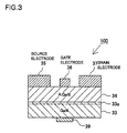
- Fig. 3 is a schematic sectional view illustrating an example of a field effect transistor according to an embodiment of the present invention
- Fig. 4 is a schematic sectional view illustrating the field effect transistor of Fig. 3 to which an inter-drain-source voltage V DS is applied and, by doing so, illustration is made of a state wherein a drain current I D flows
- Fig. 1 is a schematic sectional view illustrating an example of a conventional HEMT structure that stands on the use of a GaN compound
- Fig. 2A and 2B are schematic sectional views illustrating an example of another conventional HEMT structure that stands on the use of an GaN compound
- Fig. 3 is a schematic sectional view illustrating an example of a
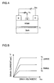
- FIG. 5 is a graphic diagram illustrating a state wherein the drain current I D flowing depending on the inter-drain-source voltage V DS is controlled by applying a gate voltageV G ;
- Fig. 6 is a band gap view illustrating a band gap between each layer in the structure of Fig. 3;
- Fig. 7A is a schematic plan view bonding the field effect transistor illustrated in Fig. 3 onto a support substrate;
- Fig. 7B is a schematic sectional view bonding the field effect transistor illustrated in Fig. 3 onto a support substrate;
- Fig. 8A-8C are schematic sectional views illustrating a manufacturing step for the field effect transistor according to an embodiment of the present invention;
- Fig. 9A-9B are schematic plan views illustrating an example of the field effect transistor according to an embodiment of the present invention;
- Fig. 9C is a schematic sectional view illustrating an example of the field effect transistor according to an embodiment of the present invention.
- Fig. 3 illustrates an example constructing a GaN-based HEMT 100, as the field effect transistor according to an embodiment of the present invention.
- the HEMT 100 illustrated in this figure has a construction in which a carrier transit layer 33 as a first semiconductor layer and a carrier supply layer 34 as a second semiconductor layer are sequentially laminated. On an upper surface of the carrier supply layer 34, there are formed a source electrode 35, gate electrode 36, and drain electrode 37.
- a monopolar device that uses electrons as the carriers will be explained.
- the device can be made a transistor using the holes.
- the carriers of a conductivity opposite to that of the carriers, i.e., electrons are discharged via the second electrode.
- the carrier supply layer 34 supplies electrons to the carrier transit layer 33.
- the electrons that have been supplied transit through a channel 33a formed at an upper portion of the carrier transit layer 33 close to the carrier supply layer 34, with a high mobility.
- the carrier transit layer 33 that is a semiconductor layer having the channel 33a acts as the electron transit layer.
- the semiconductor layer having the channel 33a referred to here in this specification means a layer that is physically substantially the same as the channel 33a.
- the dimension of the channel 33a is controlled by the depletion layer that is formed by the gate voltage applied to the gate electrode 36.
- the carrier transit layer 33 there is used an undoped GaN layer and as the carrier supply layer 34 there is used the n-type AlGaN layer.
- a dopant is doped for increasing the carrier density, it is also possible, by reducing the amount of impurity doped, or by making the layer an undoped one, to decrease the gate leak current and make the withstand voltage high.
- the carrier transit layer it may be doped with a suitable dopant, so as to decrease the transit of the carriers in the carrier transit layer 33 other than the channel 33a.
- an n - -type one is preferable. In this way, the off characteristic can be controlled depending on the carrier concentration of the carrier layer 33. Also, in the case of a normally-off type, using an i-type layer, for example, an undoped layer as the carrier transit layer 33 is preferable.
- the nitride-based compound semiconductor since when forming the nitride-based compound semiconductor it is likely that it comes to have an n-type conductivity due to the vacancy of nitrogen, doping a p-type impurity to such an extent as to compensate for that vacancy also is possible. Also, although in Fig. 3 the thickness of the AlGaN layer and that of GaN layer are similar, in an actual field effect transistor the GaN layer is greater in thickness than the AlGaN layer.
- the source electrode and drain electrode each are ohmic electrodes, and the gate electrode is a Schottky electrode.
- the gate electrode is a Schottky electrode.
- the source electrode and drain electrode construct ohmic electrodes at the interface with the ohmic contact layer formed on the carrier supply layer, while the gate electrode has a Schottky junction characteristic at the interface contacting with the Schottky contact layer formed on the carrier supply layer.
- the drain current I D can be controlled by the gate voltage V G .
- the Schottky contact layer right beneath the gate electrode acts as a barrier layer for suppressing the electric current (gate leak current) flowing between the gate electrode and the channel.
- the ohmic contact layers act to decrease those contact resistances of the source electrode and drain electrode which have been deemed as the ohmic electrodes.
- the second electrode 39 On the underside of the carrier transit layer 33 there is formed the second electrode 39. As a result of this, it is possible to draw off the holes h, having occurred due to the collision ionization, to outside the field effect transistor device via the second electrode 39. As a result of the fact that the accumulation of the holes is avoided, the avalanche effect that leads to the breakdown of the device is avoided, and thus the enhancement in the withstand voltage of the device is realized.
- the second electrode 39 doesn't need to be formed over the whole of the underside of the carrier transit layer 33. The discharge of the holes becomes possible simply by locally providing the second electrode 39 at an arbitrary position.
- the second electrode 39 may be formed over the whole of the underside of the carrier transit layer 33 or channel 33a, or alternatively, a structure wherein the electrode is provided on the substrate using a conductive substrate may be made. By making small the area of the second electrode 39, it is possible to decrease the capacitance.
- the second electrode is located at a position of the back side of the device where the gate electrode opposes or its proximity.
- the second electrode be shifted toward the drain electrode side from the position opposing the gate electrode.
- the electrodes need only to be disposed so that the center portion of the width of the second electrode may be displaced in the direction of the transit with respect to the center portion of the gate electrode.
- a one-dot chain line of Fig. 8C indicates the center portion of the width of each of the gate electrode 36 and second electrode 39.
- the material quality, film thickness, etc. are set so that it may form a Schottky contact with the carrier transit layer 33.
- a contact layer, etc. may be interposed between the second electrode 39 and the carrier transit layer 33.
- Fig. 6 there is illustrated a band gap view between each layer in the structure of Fig. 3.
- the holes h that have occurred due to the collision ionization become able to be discharged from the field effect transistor device by way of the second electrode 39.
- the holes h can be exhausted even in the ohmic contact, the holes h can more easily be exhausted in the Schottky contact.
- the second electrode be located at a position that opposes the gate electrode almost at or close to the back side of the device. Furthermore, even when the second electrode is located almost at or close to the back side of the device, it is preferable that the second electrode be shifted toward the drain electrode side from the position opposing the gate electrode.
- the second electrode may be formed at the position opposing the source electrode or drain electrode, by providing the second electrode at a position spaced away from the position that opposes the gate electrode almost at or close to the back side of the device, the holes have difficulty in moving. In addition, extreme difficulty is encountered in obtaining the effect of discharging the holes.
- the GaN-based HEMT is constructed using a gallium nitride-based compound semiconductor. According to the necessity, on the substrate there is formed a buffer layer. Further, the carrier transit layer 33 and carrier supply layer 34 are sequentially epitaxially grown. Further, the electrodes are laminated. As the method for crystal growth, it is possible to use, for example, an MOCVD (metal-organic chemical vapor deposition), HVPE (hydride vapor phase epitaxy), MBE (molecularbeam epitaxy), etc.
- MOCVD metal-organic chemical vapor deposition
- HVPE hydride vapor phase epitaxy
- MBE molecularbeam epitaxy
- the gallium nitride-based compound semiconductor is expressed by a general formula of In x Al y Ga 1-x-y N (0 ⁇ x, 0 ⁇ y, and x + y ⁇ 1).
- the n-type nitride semiconductor layer and p-type nitride semiconductor layer are each not particularly limited, namely, may each be used as a monolayer or as a multilayer structure.
- an n-type impurity and p-type impurity are suitably contained in the nitride semiconductor layer.
- the n-type impurity it is possible to use the elements belonging to the IV group that includes Si, Ge, Sn, S, O, Ti, and Zr, or the VI group,.
- Si is possible to use Si.
- the p-type impurity although not particularly limited, there can be taken up, as an example, Be, Zn, Mn, Cr, Mg, Ca, and such. Preferably, Mg is used.
- the substrate it is possible to use a conductive substrate such as GaN substrate or SiC substrate, or the like, which the thermal conduction of that is high and the heat dissipation property of that is excellent. Insulating substrate such as sapphire substrate may also be employed.
- Each of the electrodes such as the source electrode 35, gate electrode 36, or drain electrode 37 is formed using composition ingredients typically different from those used to form the semiconductor materials constructing the device.
- it is constructed using the material having excellent electric conductivity such as Ti, Al, Cu, W, Au, Ag, Mo, Ni, Pt, In, Rh, Ir, and Cr.
- the relevant material is not limited to metallic materials, and electrically conductive oxides, electrically conductive plastics materials having electric conductivity, etc. can also be used.
- the electrode it can be constructed using not only single-elemental material but also a multi-elemental material such as alloyed material, eutectic material, and mixed crystal. For example an ITO, etc. can be used.
- a structure having more than one layer can also be adopted.
- a Ti/Al electrode can be adopted, while, as the Schottky electrode, there is adopted an electrode formed using a Ni/Au material.
- the ohmic characteristic, Schottky characteristic, etc. which are demanded as the electrode for HEMT use excellently function.
- Ti/Pt, Ti/Au, and Ti/Al based metals are used and, at this time, quick annealing is performed at 800°C to 950°C.
- Ni/Au, TiN, Ti/Pd/Au, W/Au, etc. are used for the gate electrode.
- shape of the electrode although it is not particularly limited to a T-shape, I-shape, etc., by shaping into the T-shaped gate electrode, it causes the increase in the sectional area of the electrode to enable decreasing the electric resistance. Accordingly, it is further preferable in terms of the improvement in the high frequency characteristic of the operating frequency.
- a pad electrode may be formed at the surface of contact with the semiconductor layer. On the pad electrode, there is formed a metallized layer (bump) for connection to an external electrode, etc.
- the metallized layer is formed using material such as Ag, Au, Sn, In, Bi, Cu, and Zn.
- the electrode formation surface side of the field effect transistor is made to oppose external electrodes provided on a sub-mount, then the two electrodes are joined together by the bump through the use of the bump. Further, wiring etc. is performed on the sub-mount. Also, as the sub-mount, an electrically conductive substrate may be used, and the electrodes may be electrically connected to the substrate so that electric current may be taken out. As the electrode connected to the substrate, use of the source electrode is preferable. It is to be noted that, in the specification of the invention of this application, the terminology of, for example, Ti/AI indicates a structure in which Ti and Al are sequentially laminated from the semiconductor side.
- the substrate and buffer layer are preferably removed. Due to the existence of the buffer layer the leak current occurs and, as a result, a leak path is formed. Accordingly, the formation of this leak path can be prevented by removing the buffer layer. Also, the buffer layer, underlying layer, etc. at an early stage of the growth have the tendency of becoming inferior in crystallinity. In that case, because that portion serves as the leak path, it is preferable that the layers be removed at a level below which crystallinity is inferior so that the first semiconductor layer and second semiconductor layer may be formed. Regarding the substrate, when an entire substrate is removed, removal of the buffer layer and formation of the second electrode become easy. It is also possible to remove only a part of the substrate and cause exposure of the semiconductor layer and form the second electrode on the exposed part. At this time, since the hole-discharging function and characteristic can be varied according to the thickness of the first semiconductor layer in the elemental structure, i.e., the carrier transit layer, it is possible to adjust to a desired value of film thickness.
- Fig. 7A and Fig. 7B are schematic views taken in a case where the field effect transistor of Fig. 3 is bonded, or glued, to a support substrate.
- Fig. 7A is a schematic plan view
- Fig. 7B is a schematic sectional view.
- Figs. 8A to 8C are schematic sectional views illustrating the manufacturing steps for the field effect transistor of Figs. 7A and 7B.
- the MOCVD the GaN-based HEMT is fabricated on the sapphire substrate.
- the sapphire substrate is set in an MOCVD reactor as a growth substrate 81. Then, a substrate surface which is a C-plane of the sapphire substrate 81 is heated, within an atmosphere of hydrogen and, by doing so, the temperature of the substrate is elevated up to 1050°C and, while hydrogen is being caused to flow, cleaning of the substrate 81 is performed. Subsequently, the temperature of the substrate is lowered down to 510°C. Then, by using hydrogen as the carrier gas and by using as source gases a TMG (trimethyl gallium) and ammonium gas, the buffer layer 82 consisting of GaN is grown on the substrate 81 to a film thickness of approximately 200 ⁇ .
- a TMG trimethyl gallium
- the buffer layer 82 is grown, in subsequence, only the TMG (trimethyl gallium) is stopped and the temperature of the substrate is elevated up to 1050°C.
- TMG trimethyl gallium
- an undoped GaN layer is grown with a film thickness of 3 ⁇ m GaN layer.
- This undoped GaN layer acts as the carrier transit layer 33.
- the layer that is represented by the terminology "the undoped” means the one the impurity concentration of that is 1 ⁇ 10 17 /cm 3 or less.
- an undoped AlGaN layer made of Al 0.2 Ga 0.8 N the mole fraction Al ratio of which is 0.2 is grown to a film thickness of 50 ⁇ .
- the undoped GaN, undoped AlGaN, and n-type AlGaN are provided sequentially from the substrate, for brevity of the explanation no illustration is made of the undoped AlGaN.
- the undoped AlGaN it is possible to make higher electron mobility in the channel.
- a resist is coated. After this, exposure of the pattern is performed to pattern the resist. Then, for the purpose of, using a plasma RIE device, etching each of the AlGaN layer and GaN layer as the elemental isolation, etching is performed, with a CI 2 gas, using an ICP etching device. And, the source electrode 35 and drain electrode 37 are formed in such a manner as Ti and Al are treated, each, using a magnetron sputter device. By this, the Ti is sputtered to 100 ⁇ and the Al is sputtered, with 500 W, to 3000 ⁇ . After that, lift-off is done. After that, the electrodes are annealed for 10 minutes at 600°C in an atmosphere of nitrogen gas.
- the pad electrodes 40a and 40c provided on the source electrode 35 and drain electrode 37 for external connection and gate electrode 36 are separately patterned.
- the gate electrode 36 Ni is sputtered to 2000 ⁇ and is lifted off. Then, further, photolithographing is done. Further, as the pad electrode 40a and 40c, the Ni is sputtered to 2000 ⁇ and then is lifted off. Over the entire surface, the insulating protective films 72, SiN /SiO 2 are formed to 1000/20000 ⁇ .
- the metal materials for the adhesion layer 73 Ti/Pt/Au/Sn/Au are sputtered over the entire surface. As illustrated in Fig. 8A, the mass prepared by sputtering Ti/Pt/Au to the support substrate 71 Cu-W for lamination is press bonded to the above-described Ti/Pt/Au/Sn/Au surface.
- the sapphire substrate 81 is removed through the laser lift-off operation and the buffer layer 82 and part of the underlying layer are removed by polishing, as illustrated in Fig. 8B. Then the resist is patterned to the carrier transit layer 33 that has been exposed and, partially removing the elementary structure as illustrated in Fig. 8C, using the ICP etching, part of the gate electrode 36 which doubles as the pad electrode and the pad electrode 40a and 40c are exposed to made a external-connection portion 41a, 41c and 41d, shown in Fig. 7A.
- the external-connection portion 41a, 41c and 41d is exposed so that, in the side surfaces of the elemental structure that has been fabricated, the exposed portions may be extended from the component sides that are individually different from one another.
- this structure it becomes a type wherein the external-connection portion 41a, 41c and 41d of each electrode can be spatially separated apart from each other; the wires distributed from the electrode are not short-circuited; and electric discharge between the wires can be prevented.
- each electrode may be exposed so that two or more of the electrodes may be extended from the same composing side and direction.
- the gate electrode 36 and the external-connection portion of the second electrode 39 By disposing the gate electrode 36 and the external-connection portion of the second electrode 39 so that they may be extended from the same composing side and be overlapped with each other, they can be connected to each other by means of, for example, a metal layer, and thus electric connection between these becomes easy. After the performance of the etching, it is also possible to form a protective film on the exposed surface of the elemental structure 74. On the surface of the carrier transit layer 33 that opposes the gate electrode 36, a Ni Schottky electrode is formed as the second electrode 39. In Fig. 8C, the center portion in widthwise direction of the second electrode 39 is displaced, to the drain electrode 37 side along the direction of transit, when it is viewed with respect to the center portion of the gate electrode 36.
- the elemental structure and electrode structure formed adhered to the support substrate can be made up into a structure such as that illustrated in the plan view of Fig. 7A and in the sectional view of Fig. 7B.
- the sectional structure on the principal surface side of the elemental structure there are provided, as the primary electrode, the source, gate, and drain electrodes, while, on the other hand, on the other principal surface, as the secondary electrode, there is provided the second electrode, and thus a structure is prepared in which the electrodes on the primary electrode side are adhered to the support substrate 71 via the insulating film 72 and the contact layer 73.
- the structure is made up into the one in which, as illustrated in Fig.
- the external-connection portions 41a and 41c for primary electrode is embedded in the insulating film 72, and thus, the external-connection portions 41a and 41c are formed in a state of their being isolated from each other.
- the secondary electrode side and the second electrode are formed in such a manner as to extend on the insulating film 72, and thus, the structure is prepared in which the primary and secondary electrode are disposed on the insulating film 72.
- the insulating film can be formed only on a specific electrode and the electrode is conducted to the support substrate without forming insulating film, and the electrode can be taken out from the support substrate side.
- the source electrode is preferable.
- the source electrode 35 can be taken out from the support substrate 71 side.
- the pad electrode 40a for the source electrode 35 is not exposed from the elemental structure, and the external-connection portion is not formed.
- the second electrode can be also disposed in such a manner as to overlap upon the source electrode and gate electrode that oppose with the elemental structure 74 in between and be also connected to it in that manner. For example, as illustrated in Fig.
- the second electrode 39 may be formed so as to have an electrode-connection portion 42 overlapping with the external-connection portion 41a of the source electrode 35 and, by means of the electrode-connection portion 42, the second electrode 39 needs only to be electrically connected to the source electrode 35. Further, as shown in Fig. 9B, the second electrode 39 and source electrode 35 may be connected using interconnect metal 43.
- the primary electrode and the secondary electrode are disposed so as to oppose each other with the elemental structure 74 in between, because it suffices that on each electrode there are provided the gate electrode and the second electrode, as the other electrode there may be used the primary electrode previously described, or, in addition, there may also be used the secondary electrode.
- the electrode can be formed by adjusting that position.
- the positional relationship between the second electrode and either the source electrode or gate electrode of the embodiment can be established as desired. By applying this, it is possible to measure and evaluate the device characteristics resulting from the source, gate and drain electrodes of the primary electrode, and then, to adjust the position, width, area, and such of the second electrode of the secondary electrode for adjusting these characteristics, and to form the second electrode.
- a structure can be made up in which the elemental structure 74 is removed with its depth partly left as is and in the film thickness region, where that part is left as is, an opening for exposing the electrode is provided. For example, at the position that is deeper than the carrier transit layer 33, with its portion partly left as is the semiconductor layer is exposed, and part of this exposed portion is further removed to cause exposure of the electrode and this exposed portion is used as the portion of connection to the outside.
- an in-plane structure can be made up in which a interconnect metal, wherein the interconnect metal is distributed on the exposed portion of the semiconductor layer on an insulating film, is provided, and, on the exposed portion of the semiconductor layer, respective electrodes are disposed as described above.
- the manufacturing steps such as the removal step, on-the-exposed-portion insulating film formation step, etc. increase in number.
- the structure becomes the one that is inferior in terms of the insulation structure.
- the pad electrode was exposed, the source, gate, and drain electrodes may be directly exposed.
- the pad electrode portion located below the electrode it is also possible to form the portion of connection to the outside.
- the illustrated structure is made up from the standpoint of the electrode strength.
- connection circuit that uses a second electrode and in that the second electrode is directly connected to the gate electrode and source electrode
- connecting to the source electrode is more preferable.
- the source electrode may be connected to the ground and the ground and the second electrode need only to be connected together.
- To the second electrode means for applying a voltage may be provided. By applying a voltage to the second electrode, the discharge of the holes can be controlled.
- the circuit structure like this can also be made the one having a structure wherein elements such as a circuit, respective driving means, voltage-applying means, etc. have been integrated on the insulating film exposed from the elemental structure.
- a chip is mounted on the package.
- a wire bonder is used.
- heat dissipation can be made from the electrode by way of the wire.
- the inductance component can be adjusted, so that matching of the operation can be achieved. Accordingly, wire bonding is preferable.
- the external-connection portions 41a and 41c for the respective electrodes are oriented in the same side. Accordingly, regarding any of the electrodes, they can be connected from the second electrode 39 side, so that wire bonding can easily be carried out.
- the field effect transistor and a method of manufacturing the same can be utilized for, for example, the HEMT structure whose carrier transit layer has high electron mobility or a flip-chip type high mobility transistor that has a facedown structure.
- the present embodiment is therefore illustrative and not restrictive, since the scope of the invention is defined by the appended claims rather than by the description preceding them, and all changes that fall within metes and bounds of the claims, or equivalence of such metes and bounds thereof are therefore intended to be embraced by the claims.
Landscapes
- Junction Field-Effect Transistors (AREA)
Applications Claiming Priority (2)
| Application Number | Priority Date | Filing Date | Title |
|---|---|---|---|
| JP2004336516 | 2004-11-19 | ||
| JP2005329267A JP4650224B2 (ja) | 2004-11-19 | 2005-11-14 | 電界効果トランジスタ |
Publications (3)
| Publication Number | Publication Date |
|---|---|
| EP1659622A2 true EP1659622A2 (de) | 2006-05-24 |
| EP1659622A3 EP1659622A3 (de) | 2008-04-16 |
| EP1659622B1 EP1659622B1 (de) | 2016-10-19 |
Family
ID=36000945
Family Applications (1)
| Application Number | Title | Priority Date | Filing Date |
|---|---|---|---|
| EP05292446.1A Expired - Lifetime EP1659622B1 (de) | 2004-11-19 | 2005-11-18 | Feldeffekttransistor und Verfahren zu seiner Herstellung |
Country Status (3)
| Country | Link |
|---|---|
| US (1) | US7508014B2 (de) |
| EP (1) | EP1659622B1 (de) |
| JP (1) | JP4650224B2 (de) |
Cited By (1)
| Publication number | Priority date | Publication date | Assignee | Title |
|---|---|---|---|---|
| WO2023100058A1 (en) * | 2021-12-05 | 2023-06-08 | International Business Machines Corporation | A high electron mobility transistor with source and drain electrodes below the channel |
Families Citing this family (67)
| Publication number | Priority date | Publication date | Assignee | Title |
|---|---|---|---|---|
| JP5087818B2 (ja) * | 2005-03-25 | 2012-12-05 | 日亜化学工業株式会社 | 電界効果トランジスタ |
| JP2007149794A (ja) * | 2005-11-25 | 2007-06-14 | Matsushita Electric Ind Co Ltd | 電界効果トランジスタ |
| JP2008078604A (ja) * | 2006-08-24 | 2008-04-03 | Rohm Co Ltd | Mis型電界効果トランジスタおよびその製造方法 |
| JP2008053448A (ja) * | 2006-08-24 | 2008-03-06 | Rohm Co Ltd | Mis型電界効果トランジスタおよびその製造方法 |
| JP5183913B2 (ja) * | 2006-11-24 | 2013-04-17 | 住友電工デバイス・イノベーション株式会社 | 半導体装置の製造方法 |
| WO2008099949A1 (ja) * | 2007-02-16 | 2008-08-21 | Sumitomo Chemical Company, Limited | 電界効果トランジスタ用エピタキシャル基板 |
| JP4691060B2 (ja) | 2007-03-23 | 2011-06-01 | 古河電気工業株式会社 | GaN系半導体素子 |
| US7915643B2 (en) | 2007-09-17 | 2011-03-29 | Transphorm Inc. | Enhancement mode gallium nitride power devices |
| US20090072269A1 (en) * | 2007-09-17 | 2009-03-19 | Chang Soo Suh | Gallium nitride diodes and integrated components |
| US8304809B2 (en) | 2007-11-16 | 2012-11-06 | Furukawa Electric Co., Ltd. | GaN-based semiconductor device and method of manufacturing the same |
| JP2009267358A (ja) | 2008-04-03 | 2009-11-12 | Toshiba Corp | 半導体装置 |
| US8519438B2 (en) | 2008-04-23 | 2013-08-27 | Transphorm Inc. | Enhancement mode III-N HEMTs |
| US8343824B2 (en) * | 2008-04-29 | 2013-01-01 | International Rectifier Corporation | Gallium nitride material processing and related device structures |
| US8471075B2 (en) * | 2008-07-31 | 2013-06-25 | Celanese International Corporation | Processes for making ethanol from acetic acid |
| JP5207874B2 (ja) * | 2008-08-08 | 2013-06-12 | 親夫 木村 | 半導体装置およびその製造方法 |
| JP5388514B2 (ja) * | 2008-09-09 | 2014-01-15 | 株式会社東芝 | 半導体装置及び半導体装置の製造方法 |
| US8289065B2 (en) | 2008-09-23 | 2012-10-16 | Transphorm Inc. | Inductive load power switching circuits |
| JP5608969B2 (ja) * | 2008-10-20 | 2014-10-22 | 富士通株式会社 | 化合物半導体装置及びその製造方法 |
| US7898004B2 (en) | 2008-12-10 | 2011-03-01 | Transphorm Inc. | Semiconductor heterostructure diodes |
| JP2010232279A (ja) * | 2009-03-26 | 2010-10-14 | Furukawa Electric Co Ltd:The | 電界効果トランジスタ |
| US8742459B2 (en) | 2009-05-14 | 2014-06-03 | Transphorm Inc. | High voltage III-nitride semiconductor devices |
| JP5487749B2 (ja) | 2009-06-17 | 2014-05-07 | 富士通株式会社 | 半導体装置及びその製造方法 |
| WO2011005444A1 (en) * | 2009-06-22 | 2011-01-13 | Raytheon Company | Gallium nitride for liquid crystal electrodes |
| JP5564842B2 (ja) | 2009-07-10 | 2014-08-06 | サンケン電気株式会社 | 半導体装置 |
| JP2011040676A (ja) * | 2009-08-18 | 2011-02-24 | Sanken Electric Co Ltd | 半導体装置及びその製造方法 |
| US8390000B2 (en) | 2009-08-28 | 2013-03-05 | Transphorm Inc. | Semiconductor devices with field plates |
| KR20120081072A (ko) * | 2009-09-07 | 2012-07-18 | 스미또모 가가꾸 가부시키가이샤 | 전계 효과 트랜지스터, 반도체 기판, 전계 효과 트랜지스터의 제조 방법, 및 반도체 기판의 제조 방법 |
| KR101632314B1 (ko) | 2009-09-11 | 2016-06-22 | 삼성전자주식회사 | 전계 효과형 반도체 소자 및 그 제조 방법 |
| US8389977B2 (en) | 2009-12-10 | 2013-03-05 | Transphorm Inc. | Reverse side engineered III-nitride devices |
| US20110147796A1 (en) * | 2009-12-17 | 2011-06-23 | Infineon Technologies Austria Ag | Semiconductor device with metal carrier and manufacturing method |
| KR101774933B1 (ko) * | 2010-03-02 | 2017-09-06 | 삼성전자 주식회사 | 듀얼 디플리션을 나타내는 고 전자 이동도 트랜지스터 및 그 제조방법 |
| JP5707786B2 (ja) | 2010-08-31 | 2015-04-30 | 富士通株式会社 | 化合物半導体装置及びその製造方法 |
| KR20120027987A (ko) * | 2010-09-14 | 2012-03-22 | 삼성엘이디 주식회사 | 질화갈륨계 반도체소자 및 그 제조방법 |
| US8742460B2 (en) | 2010-12-15 | 2014-06-03 | Transphorm Inc. | Transistors with isolation regions |
| US8643062B2 (en) | 2011-02-02 | 2014-02-04 | Transphorm Inc. | III-N device structures and methods |
| US8716141B2 (en) | 2011-03-04 | 2014-05-06 | Transphorm Inc. | Electrode configurations for semiconductor devices |
| US8772842B2 (en) | 2011-03-04 | 2014-07-08 | Transphorm, Inc. | Semiconductor diodes with low reverse bias currents |
| US9214538B2 (en) * | 2011-05-16 | 2015-12-15 | Eta Semiconductor Inc. | High performance multigate transistor |
| US8901604B2 (en) | 2011-09-06 | 2014-12-02 | Transphorm Inc. | Semiconductor devices with guard rings |
| US9257547B2 (en) | 2011-09-13 | 2016-02-09 | Transphorm Inc. | III-N device structures having a non-insulating substrate |
| US8598937B2 (en) | 2011-10-07 | 2013-12-03 | Transphorm Inc. | High power semiconductor electronic components with increased reliability |
| US9165766B2 (en) | 2012-02-03 | 2015-10-20 | Transphorm Inc. | Buffer layer structures suited for III-nitride devices with foreign substrates |
| WO2013155108A1 (en) | 2012-04-09 | 2013-10-17 | Transphorm Inc. | N-polar iii-nitride transistors |
| KR101928814B1 (ko) * | 2012-05-04 | 2018-12-14 | 한국전자통신연구원 | 질화물계 화합물 전력반도체 장치 및 그 제조 방법 |
| US9184275B2 (en) | 2012-06-27 | 2015-11-10 | Transphorm Inc. | Semiconductor devices with integrated hole collectors |
| JP6522521B2 (ja) | 2013-02-15 | 2019-05-29 | トランスフォーム インコーポレーテッド | 半導体デバイスの電極及びその製造方法 |
| US9087718B2 (en) | 2013-03-13 | 2015-07-21 | Transphorm Inc. | Enhancement-mode III-nitride devices |
| US9245993B2 (en) | 2013-03-15 | 2016-01-26 | Transphorm Inc. | Carbon doping semiconductor devices |
| JP6171850B2 (ja) * | 2013-04-30 | 2017-08-02 | 豊田合成株式会社 | 半導体装置およびその製造方法 |
| US9443938B2 (en) | 2013-07-19 | 2016-09-13 | Transphorm Inc. | III-nitride transistor including a p-type depleting layer |
| US9318593B2 (en) | 2014-07-21 | 2016-04-19 | Transphorm Inc. | Forming enhancement mode III-nitride devices |
| EP3192101A4 (de) * | 2014-09-09 | 2018-05-23 | Intel Corporation | Multigate-transistoren mit hoher elektronenmobilität und verfahren zur herstellung |
| US9536967B2 (en) | 2014-12-16 | 2017-01-03 | Transphorm Inc. | Recessed ohmic contacts in a III-N device |
| US9536966B2 (en) | 2014-12-16 | 2017-01-03 | Transphorm Inc. | Gate structures for III-N devices |
| EP3038177B1 (de) | 2014-12-22 | 2019-12-18 | Nokia Technologies Oy | Modulare elektronische Vorrichtungen und Verfahren |
| US10867834B2 (en) * | 2015-12-31 | 2020-12-15 | Taiwan Semiconductor Manufacturing Company Ltd. | Semiconductor structure and manufacturing method thereof |
| JP6888013B2 (ja) | 2016-01-15 | 2021-06-16 | トランスフォーム テクノロジー,インコーポレーテッド | AL(1−x)Si(x)Oゲート絶縁体を有するエンハンスメントモードIII族窒化物デバイス |
| WO2017210323A1 (en) | 2016-05-31 | 2017-12-07 | Transphorm Inc. | Iii-nitride devices including a graded depleting layer |
| JP6769322B2 (ja) * | 2017-02-06 | 2020-10-14 | 富士通株式会社 | 半導体装置、電源装置及び増幅器 |
| US11508821B2 (en) | 2017-05-12 | 2022-11-22 | Analog Devices, Inc. | Gallium nitride device for high frequency and high power applications |
| WO2020010253A1 (en) | 2018-07-06 | 2020-01-09 | Analog Devices, Inc. | Compound device with back-side field plate |
| CN110010682B (zh) * | 2019-03-22 | 2024-08-02 | 华南理工大学 | 具有三明治结构的GaN-HEMT器件及其制备方法 |
| JP7553915B2 (ja) * | 2020-04-15 | 2024-09-19 | 国立大学法人東海国立大学機構 | 窒化ガリウム半導体装置の製造方法 |
| WO2021229734A1 (ja) | 2020-05-14 | 2021-11-18 | 三菱電機株式会社 | 半導体装置および半導体装置の製造方法 |
| US11450749B2 (en) | 2020-05-27 | 2022-09-20 | Taiwan Semiconductor Manufacturing Company, Ltd. | Electrode structure for vertical group III-V device |
| CN114695114B (zh) * | 2022-05-31 | 2022-09-09 | 中芯越州集成电路制造(绍兴)有限公司 | 半导体器件及其制作方法 |
| FR3159875A1 (fr) * | 2024-02-29 | 2025-09-05 | Stmicroelectronics International N.V. | Dispositif électronique |
Citations (3)
| Publication number | Priority date | Publication date | Assignee | Title |
|---|---|---|---|---|
| JPH02148739A (ja) | 1988-11-29 | 1990-06-07 | Mitsubishi Electric Corp | 半導体装置の製造方法 |
| JP2001168111A (ja) | 1999-12-07 | 2001-06-22 | Nippon Telegr & Teleph Corp <Ntt> | GaN電界効果トランジスタ |
| WO2004068590A1 (en) | 2003-01-29 | 2004-08-12 | Kabushiki Kaisha Toshiba | Power semiconductor device |
Family Cites Families (34)
| Publication number | Priority date | Publication date | Assignee | Title |
|---|---|---|---|---|
| FR2557368B1 (fr) * | 1983-12-27 | 1986-04-11 | Thomson Csf | Transistor a effet de champ, de structure verticale submicronique, et son procede de realisation |
| US4616242A (en) * | 1985-05-08 | 1986-10-07 | International Business Machines Corporation | Enhancement and depletion mode selection layer for field effect transistor |
| FR2600821B1 (fr) * | 1986-06-30 | 1988-12-30 | Thomson Csf | Dispositif semi-conducteur a heterojonction et double canal, son application a un transistor a effet de champ, et son application a un dispositif de transductance negative |
| US4821093A (en) * | 1986-08-18 | 1989-04-11 | The United States Of America As Represented By The Secretary Of The Army | Dual channel high electron mobility field effect transistor |
| US5172194A (en) * | 1987-09-16 | 1992-12-15 | National Science Council | Structures of modulation doped base hot electron transistors |
| JP3162424B2 (ja) * | 1991-05-27 | 2001-04-25 | キヤノン株式会社 | 導波型光検出器及びその作製方法 |
| US5359220A (en) * | 1992-12-22 | 1994-10-25 | Hughes Aircraft Company | Hybrid bipolar/field-effect power transistor in group III-V material system |
| DE4322650A1 (de) * | 1993-07-07 | 1995-01-12 | Siemens Ag | Temperatursensor mit einem p-n-Übergang |
| JP3186405B2 (ja) * | 1994-03-08 | 2001-07-11 | 富士電機株式会社 | 横型mosfet |
| US5399887A (en) * | 1994-05-03 | 1995-03-21 | Motorola, Inc. | Modulation doped field effect transistor |
| KR0135804B1 (ko) * | 1994-06-13 | 1998-04-24 | 김광호 | 실리콘 온 인슐레이터(soi) 트랜지스터 |
| US5838029A (en) * | 1994-08-22 | 1998-11-17 | Rohm Co., Ltd. | GaN-type light emitting device formed on a silicon substrate |
| US5777353A (en) * | 1995-11-09 | 1998-07-07 | National Science Council | Multiple-function gaas transistors with very strong negative differential resistance phenomena |
| JPH09252112A (ja) * | 1996-03-14 | 1997-09-22 | Toshiba Corp | 高電子移動度トランジスタ及びiii−v族化合物半導体デバイス |
| JP3458611B2 (ja) * | 1996-08-28 | 2003-10-20 | ソニー株式会社 | Soi型半導体装置の製造方法 |
| US5825049A (en) * | 1996-10-09 | 1998-10-20 | Sandia Corporation | Resonant tunneling device with two-dimensional quantum well emitter and base layers |
| DE19714054A1 (de) * | 1997-04-05 | 1998-10-08 | Daimler Benz Ag | SiGe-Photodetektor mit hohem Wirkungsgrad |
| JP2000091349A (ja) * | 1998-09-10 | 2000-03-31 | Nippon Telegr & Teleph Corp <Ntt> | 半導体装置の製作方法 |
| US6720589B1 (en) * | 1998-09-16 | 2004-04-13 | Kabushiki Kaisha Toshiba | Semiconductor device |
| JP3129298B2 (ja) * | 1998-11-11 | 2001-01-29 | 日本電気株式会社 | 電界効果トランジスタ及びその製造方法 |
| JP2001284576A (ja) * | 2000-03-30 | 2001-10-12 | Toshiba Corp | 高電子移動度トランジスタ及びその製造方法 |
| US6396085B1 (en) * | 2000-04-25 | 2002-05-28 | The Furukawa Electric Co., Ltd | GaN-type semiconductor vertical field effect transistor |
| JP2001332565A (ja) * | 2000-05-25 | 2001-11-30 | Nec Corp | 負性微分抵抗素子およびその製造方法 |
| JP2003007976A (ja) * | 2001-06-25 | 2003-01-10 | Mitsubishi Electric Corp | 半導体装置及びモジュール装置 |
| US6855970B2 (en) * | 2002-03-25 | 2005-02-15 | Kabushiki Kaisha Toshiba | High-breakdown-voltage semiconductor device |
| JP3859066B2 (ja) | 2002-04-02 | 2006-12-20 | 日本電信電話株式会社 | 半導体装置およびそれを用いた半導体回路 |
| JP4645034B2 (ja) * | 2003-02-06 | 2011-03-09 | 株式会社豊田中央研究所 | Iii族窒化物半導体を有する半導体素子 |
| JP2004241711A (ja) * | 2003-02-07 | 2004-08-26 | Matsushita Electric Ind Co Ltd | 半導体装置 |
| JP4038485B2 (ja) * | 2003-03-12 | 2008-01-23 | 三星エスディアイ株式会社 | 薄膜トランジスタを備えた平板表示素子 |
| JP4492034B2 (ja) * | 2003-04-11 | 2010-06-30 | 日亜化学工業株式会社 | Hemt及びその製造方法 |
| US7078743B2 (en) * | 2003-05-15 | 2006-07-18 | Matsushita Electric Industrial Co., Ltd. | Field effect transistor semiconductor device |
| WO2005004198A2 (en) * | 2003-06-13 | 2005-01-13 | North Carolina State University | Complex oxides for use in semiconductor devices and related methods |
| JP4509031B2 (ja) * | 2003-09-05 | 2010-07-21 | サンケン電気株式会社 | 窒化物半導体装置 |
| US7145174B2 (en) * | 2004-03-12 | 2006-12-05 | Hewlett-Packard Development Company, Lp. | Semiconductor device |
-
2005
- 2005-11-14 JP JP2005329267A patent/JP4650224B2/ja not_active Expired - Fee Related
- 2005-11-16 US US11/274,307 patent/US7508014B2/en not_active Expired - Lifetime
- 2005-11-18 EP EP05292446.1A patent/EP1659622B1/de not_active Expired - Lifetime
Patent Citations (3)
| Publication number | Priority date | Publication date | Assignee | Title |
|---|---|---|---|---|
| JPH02148739A (ja) | 1988-11-29 | 1990-06-07 | Mitsubishi Electric Corp | 半導体装置の製造方法 |
| JP2001168111A (ja) | 1999-12-07 | 2001-06-22 | Nippon Telegr & Teleph Corp <Ntt> | GaN電界効果トランジスタ |
| WO2004068590A1 (en) | 2003-01-29 | 2004-08-12 | Kabushiki Kaisha Toshiba | Power semiconductor device |
Non-Patent Citations (2)
| Title |
|---|
| TSUBAKI K. ET AL.: "Applied Physics Letters", vol. 53, 5 September 1988, AMERICAN INSTITUTE OF PHYSICS, article "Coherence Length in Quantum Interference Devices Having Periodic Potential", pages: 859 - 861 |
| WICHMANN N. ET AL.: "InAIAs/InGaAs double-gate HEMTs with high extrinsic transconductance", INDIUM PHOSPHIDE AND RELATED MATERIALS, 31 May 2004 (2004-05-31), pages 295 - 298, XP010814958, DOI: doi:10.1109/ICIPRM.2004.1442713 |
Cited By (2)
| Publication number | Priority date | Publication date | Assignee | Title |
|---|---|---|---|---|
| WO2023100058A1 (en) * | 2021-12-05 | 2023-06-08 | International Business Machines Corporation | A high electron mobility transistor with source and drain electrodes below the channel |
| US12191382B2 (en) | 2021-12-05 | 2025-01-07 | International Business Machines Corporation | High electron mobility transistor with source and drain electrodes below the channel |
Also Published As
| Publication number | Publication date |
|---|---|
| EP1659622B1 (de) | 2016-10-19 |
| EP1659622A3 (de) | 2008-04-16 |
| JP2006173582A (ja) | 2006-06-29 |
| JP4650224B2 (ja) | 2011-03-16 |
| US7508014B2 (en) | 2009-03-24 |
| US20060108602A1 (en) | 2006-05-25 |
Similar Documents
| Publication | Publication Date | Title |
|---|---|---|
| US7508014B2 (en) | Field effect transistor including a gate electrode and an additional electrode | |
| US7560752B2 (en) | Field effect transistor including two group III-V compound semiconductor layers | |
| JP5076278B2 (ja) | 電界効果トランジスタ | |
| US9236464B2 (en) | Method of forming a high electron mobility transistor | |
| TWI472036B (zh) | 化合物半導體裝置及其製造方法 | |
| US8866312B2 (en) | Semiconductor apparatus, method for manufacturing the same and electric device | |
| US12272743B2 (en) | Semiconductor device comprising a drain back contact electrode, method of manufacturing the same, and semiconductor package structure | |
| US12342562B2 (en) | High electron mobility transistor and method for forming the same using the metal gate layer and spacer as an etch mask | |
| JP2008193123A (ja) | 半導体装置 | |
| JP2004363563A (ja) | 半導体装置 | |
| JP2006269939A5 (de) | ||
| JP2010171416A (ja) | 半導体装置、半導体装置の製造方法および半導体装置のリーク電流低減方法 | |
| US12159931B2 (en) | Nitride-based semiconductor device and method for manufacturing the same | |
| JP2007305954A (ja) | 電界効果トランジスタ及びその装置 | |
| US20230352540A1 (en) | Nitride-based semiconductor device and method for manufacturing the same | |
| JP2014207379A (ja) | 化合物半導体装置及びその製造方法 | |
| CN117133806A (zh) | 一种天然超结GaN HEMT器件及其制备方法 | |
| CN115997287B (zh) | 氮化物基半导体ic芯片及其制造方法 | |
| JP2021114590A (ja) | 半導体装置、半導体装置の製造方法及び電子装置 | |
| WO2024000475A1 (en) | Semiconductor packaged device and method for manufacturing thereof | |
| WO2026023216A1 (ja) | 半導体デバイスおよびその製造方法 | |
| WO2025177918A1 (ja) | 窒化物半導体装置 | |
| JP2025002282A (ja) | 窒化物半導体装置、窒化物半導体装置の製造方法及びエピタキシャル基板 | |
| CN115812253A (zh) | 氮化物基半导体器件及其制造方法 | |
| CN118302852A (zh) | 半导体封装装置及其制造方法 |
Legal Events
| Date | Code | Title | Description |
|---|---|---|---|
| PUAI | Public reference made under article 153(3) epc to a published international application that has entered the european phase |
Free format text: ORIGINAL CODE: 0009012 |
|
| AK | Designated contracting states |
Kind code of ref document: A2 Designated state(s): AT BE BG CH CY CZ DE DK EE ES FI FR GB GR HU IE IS IT LI LT LU LV MC NL PL PT RO SE SI SK TR |
|
| AX | Request for extension of the european patent |
Extension state: AL BA HR MK YU |
|
| PUAL | Search report despatched |
Free format text: ORIGINAL CODE: 0009013 |
|
| AK | Designated contracting states |
Kind code of ref document: A3 Designated state(s): AT BE BG CH CY CZ DE DK EE ES FI FR GB GR HU IE IS IT LI LT LU LV MC NL PL PT RO SE SI SK TR |
|
| AX | Request for extension of the european patent |
Extension state: AL BA HR MK YU |
|
| RIC1 | Information provided on ipc code assigned before grant |
Ipc: H01L 21/68 20060101ALI20080313BHEP Ipc: H01L 29/20 20060101ALN20080313BHEP Ipc: H01L 21/338 20060101AFI20060320BHEP Ipc: H01L 29/778 20060101ALI20080313BHEP Ipc: H01L 29/41 20060101ALI20080313BHEP |
|
| 17P | Request for examination filed |
Effective date: 20081014 |
|
| AKX | Designation fees paid |
Designated state(s): DE FR GB |
|
| 17Q | First examination report despatched |
Effective date: 20100714 |
|
| GRAP | Despatch of communication of intention to grant a patent |
Free format text: ORIGINAL CODE: EPIDOSNIGR1 |
|
| INTG | Intention to grant announced |
Effective date: 20151120 |
|
| RIC1 | Information provided on ipc code assigned before grant |
Ipc: H01L 21/683 20060101ALI20151106BHEP Ipc: H01L 21/338 20060101AFI20151106BHEP Ipc: H01L 29/41 20060101ALI20151106BHEP Ipc: H01L 29/778 20060101ALI20151106BHEP Ipc: H01L 29/20 20060101ALN20151106BHEP |
|
| RIN1 | Information on inventor provided before grant (corrected) |
Inventor name: TANIMOTO, MASASHI |
|
| GRAP | Despatch of communication of intention to grant a patent |
Free format text: ORIGINAL CODE: EPIDOSNIGR1 |
|
| INTG | Intention to grant announced |
Effective date: 20160401 |
|
| RIC1 | Information provided on ipc code assigned before grant |
Ipc: H01L 29/41 20060101ALI20160318BHEP Ipc: H01L 29/20 20060101ALN20160318BHEP Ipc: H01L 29/778 20060101ALI20160318BHEP Ipc: H01L 21/338 20060101AFI20160318BHEP Ipc: H01L 21/683 20060101ALI20160318BHEP |
|
| GRAS | Grant fee paid |
Free format text: ORIGINAL CODE: EPIDOSNIGR3 |
|
| GRAA | (expected) grant |
Free format text: ORIGINAL CODE: 0009210 |
|
| AK | Designated contracting states |
Kind code of ref document: B1 Designated state(s): DE FR GB |
|
| REG | Reference to a national code |
Ref country code: GB Ref legal event code: FG4D |
|
| REG | Reference to a national code |
Ref country code: DE Ref legal event code: R096 Ref document number: 602005050461 Country of ref document: DE |
|
| REG | Reference to a national code |
Ref country code: DE Ref legal event code: R097 Ref document number: 602005050461 Country of ref document: DE |
|
| PLBE | No opposition filed within time limit |
Free format text: ORIGINAL CODE: 0009261 |
|
| REG | Reference to a national code |
Ref country code: FR Ref legal event code: ST Effective date: 20170731 |
|
| STAA | Information on the status of an ep patent application or granted ep patent |
Free format text: STATUS: NO OPPOSITION FILED WITHIN TIME LIMIT |
|
| 26N | No opposition filed |
Effective date: 20170720 |
|
| PG25 | Lapsed in a contracting state [announced via postgrant information from national office to epo] |
Ref country code: FR Free format text: LAPSE BECAUSE OF NON-PAYMENT OF DUE FEES Effective date: 20161219 |
|
| REG | Reference to a national code |
Ref country code: DE Ref legal event code: R082 Ref document number: 602005050461 Country of ref document: DE Representative=s name: CBDL PATENTANWAELTE GBR, DE Ref country code: DE Ref legal event code: R082 Ref document number: 602005050461 Country of ref document: DE Representative=s name: CBDL PATENTANWAELTE EGBR, DE |
|
| P01 | Opt-out of the competence of the unified patent court (upc) registered |
Effective date: 20230522 |
|
| PGFP | Annual fee paid to national office [announced via postgrant information from national office to epo] |
Ref country code: GB Payment date: 20230928 Year of fee payment: 19 |
|
| PGFP | Annual fee paid to national office [announced via postgrant information from national office to epo] |
Ref country code: DE Payment date: 20230929 Year of fee payment: 19 |
|
| REG | Reference to a national code |
Ref country code: DE Ref legal event code: R079 Ref document number: 602005050461 Country of ref document: DE Free format text: PREVIOUS MAIN CLASS: H01L0021338000 Ipc: H10D0030870000 |
|
| REG | Reference to a national code |
Ref country code: DE Ref legal event code: R119 Ref document number: 602005050461 Country of ref document: DE |
|
| GBPC | Gb: european patent ceased through non-payment of renewal fee |
Effective date: 20241118 |
|
| PG25 | Lapsed in a contracting state [announced via postgrant information from national office to epo] |
Ref country code: DE Free format text: LAPSE BECAUSE OF NON-PAYMENT OF DUE FEES Effective date: 20250603 |
|
| PG25 | Lapsed in a contracting state [announced via postgrant information from national office to epo] |
Ref country code: GB Free format text: LAPSE BECAUSE OF NON-PAYMENT OF DUE FEES Effective date: 20241118 |