EP1667117A1 - Tête magnétique à effet de magnétorésistance avec une sous-couche ayant une structure laminée d'une couche d'un metal du groupe tungstène formée sur une couche d'un metal du groupe tantale - Google Patents
Tête magnétique à effet de magnétorésistance avec une sous-couche ayant une structure laminée d'une couche d'un metal du groupe tungstène formée sur une couche d'un metal du groupe tantale Download PDFInfo
- Publication number
- EP1667117A1 EP1667117A1 EP06003898A EP06003898A EP1667117A1 EP 1667117 A1 EP1667117 A1 EP 1667117A1 EP 06003898 A EP06003898 A EP 06003898A EP 06003898 A EP06003898 A EP 06003898A EP 1667117 A1 EP1667117 A1 EP 1667117A1
- Authority
- EP
- European Patent Office
- Prior art keywords
- film
- layer
- magnetic
- head
- magnetoresistance
- Prior art date
- Legal status (The legal status is an assumption and is not a legal conclusion. Google has not performed a legal analysis and makes no representation as to the accuracy of the status listed.)
- Granted
Links
Images









Classifications
-
- G—PHYSICS
- G11—INFORMATION STORAGE
- G11B—INFORMATION STORAGE BASED ON RELATIVE MOVEMENT BETWEEN RECORD CARRIER AND TRANSDUCER
- G11B5/00—Recording by magnetisation or demagnetisation of a record carrier; Reproducing by magnetic means; Record carriers therefor
- G11B5/127—Structure or manufacture of heads, e.g. inductive
- G11B5/33—Structure or manufacture of flux-sensitive heads, i.e. for reproduction only; Combination of such heads with means for recording or erasing only
- G11B5/39—Structure or manufacture of flux-sensitive heads, i.e. for reproduction only; Combination of such heads with means for recording or erasing only using magneto-resistive devices or effects
-
- G—PHYSICS
- G11—INFORMATION STORAGE
- G11B—INFORMATION STORAGE BASED ON RELATIVE MOVEMENT BETWEEN RECORD CARRIER AND TRANSDUCER
- G11B5/00—Recording by magnetisation or demagnetisation of a record carrier; Reproducing by magnetic means; Record carriers therefor
- G11B5/127—Structure or manufacture of heads, e.g. inductive
- G11B5/33—Structure or manufacture of flux-sensitive heads, i.e. for reproduction only; Combination of such heads with means for recording or erasing only
- G11B5/39—Structure or manufacture of flux-sensitive heads, i.e. for reproduction only; Combination of such heads with means for recording or erasing only using magneto-resistive devices or effects
- G11B5/3903—Structure or manufacture of flux-sensitive heads, i.e. for reproduction only; Combination of such heads with means for recording or erasing only using magneto-resistive devices or effects using magnetic thin film layers or their effects, the films being part of integrated structures
-
- B—PERFORMING OPERATIONS; TRANSPORTING
- B82—NANOTECHNOLOGY
- B82Y—SPECIFIC USES OR APPLICATIONS OF NANOSTRUCTURES; MEASUREMENT OR ANALYSIS OF NANOSTRUCTURES; MANUFACTURE OR TREATMENT OF NANOSTRUCTURES
- B82Y10/00—Nanotechnology for information processing, storage or transmission, e.g. quantum computing or single electron logic
-
- G—PHYSICS
- G11—INFORMATION STORAGE
- G11B—INFORMATION STORAGE BASED ON RELATIVE MOVEMENT BETWEEN RECORD CARRIER AND TRANSDUCER
- G11B5/00—Recording by magnetisation or demagnetisation of a record carrier; Reproducing by magnetic means; Record carriers therefor
- G11B5/127—Structure or manufacture of heads, e.g. inductive
- G11B5/33—Structure or manufacture of flux-sensitive heads, i.e. for reproduction only; Combination of such heads with means for recording or erasing only
- G11B5/39—Structure or manufacture of flux-sensitive heads, i.e. for reproduction only; Combination of such heads with means for recording or erasing only using magneto-resistive devices or effects
- G11B5/3903—Structure or manufacture of flux-sensitive heads, i.e. for reproduction only; Combination of such heads with means for recording or erasing only using magneto-resistive devices or effects using magnetic thin film layers or their effects, the films being part of integrated structures
- G11B5/3906—Details related to the use of magnetic thin film layers or to their effects
- G11B5/3929—Disposition of magnetic thin films not used for directly coupling magnetic flux from the track to the MR film or for shielding
-
- G—PHYSICS
- G11—INFORMATION STORAGE
- G11B—INFORMATION STORAGE BASED ON RELATIVE MOVEMENT BETWEEN RECORD CARRIER AND TRANSDUCER
- G11B5/00—Recording by magnetisation or demagnetisation of a record carrier; Reproducing by magnetic means; Record carriers therefor
- G11B5/127—Structure or manufacture of heads, e.g. inductive
- G11B5/33—Structure or manufacture of flux-sensitive heads, i.e. for reproduction only; Combination of such heads with means for recording or erasing only
- G11B5/39—Structure or manufacture of flux-sensitive heads, i.e. for reproduction only; Combination of such heads with means for recording or erasing only using magneto-resistive devices or effects
- G11B5/3903—Structure or manufacture of flux-sensitive heads, i.e. for reproduction only; Combination of such heads with means for recording or erasing only using magneto-resistive devices or effects using magnetic thin film layers or their effects, the films being part of integrated structures
- G11B5/3906—Details related to the use of magnetic thin film layers or to their effects
- G11B5/3929—Disposition of magnetic thin films not used for directly coupling magnetic flux from the track to the MR film or for shielding
- G11B5/3932—Magnetic biasing films
-
- G—PHYSICS
- G11—INFORMATION STORAGE
- G11B—INFORMATION STORAGE BASED ON RELATIVE MOVEMENT BETWEEN RECORD CARRIER AND TRANSDUCER
- G11B5/00—Recording by magnetisation or demagnetisation of a record carrier; Reproducing by magnetic means; Record carriers therefor
- G11B5/127—Structure or manufacture of heads, e.g. inductive
- G11B5/31—Structure or manufacture of heads, e.g. inductive using thin films
- G11B5/3109—Details
- G11B5/3113—Details for improving the magnetic domain structure or avoiding the formation or displacement of undesirable magnetic domains
Definitions
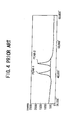
- FIG.4 shows, by using an X-ray diffraction, the hard film 106 having a deteriorated crystallinity.
- FIG.4 there occur not only a PEAK-1 based on the spin-valve film 103 but also a PEAK-2 based on a (001) surface of Co.
- This PEAK-2 indicates that there exists a crystal grain having the c-axis of Co composing the hard film 106 aligned in the direction of thickness thereof; therefore a deteriorated coercive force and a deteriorated squareness ratio can be confirmed also from FIG.4.
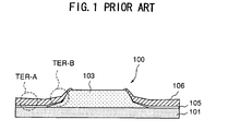
- the antiferromagnetic layer 103-1 exists under the underlying layer 105, the hard film 106 can be effectively positioned at the same height as the free magnetic layer.
- the antiferromagnetic layer 103-1 deteriorates the crystallinity of the underlying layer 105 formed thereon. Consequently, a preferable MR head cannot be formed.
- a magnetic head of a magnetoresistance type comprising:
- the magnetic head of the magnetoresistance type can provide an effective magnetic-domain regulation.
- the magnetic-domain regulating film arranged at an optimal position can have excellent magnetic characteristics; therefore, the magnetic head of the magnetoresistance type can provide a more effective magnetic-domain regulation.
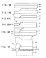
- FIG.10C shows a step of forming a hard-film underlying layer 45.
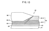
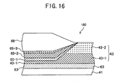
- the hard-film underlying layer 45 formed in this step has its intrinsic function of improving a crystallinity of a hard film 46 that is to be formed thereon and a function of adjusting the position of the hard film 46 in the direction of thickness so as to arrange the hard film 46 at a position corresponding to the free magnetic layer 43FR of the spin-valve film 43. That is, the hard-film underlying layer 45 according to the present embodiment not only has its intrinsic function, but also is formed so thick as to raise the bottom of the hard film 46 and thus to arrange the hard film 46 at a position corresponding to the free magnetic layer 43FR of the spin-valve film 43. Whereas the conventional hard-film underlying layer is approximately 2 to 3 nm in thickness, the hard-film underlying layer 45 according to the present embodiment is, for example, 12 to 13 nm in thickness, which is thicker than the conventional hard-film underlying layer.
- the seventh embodiment of the present invention is an MR head 70 including a spin-valve film having the regular-order laminated structure.
- the free magnetic layer 43FR in the spin-valve film of an MR head like this MR head 70 is located near the bottom of the spin-valve film, and thus in some cases, a hard film may be formed at a position shifted upward from the position of the free magnetic layer.
- the present seventh embodiment lowers the bottom of the hard film by etching and cutting out parts of the insulating layer exposed on both sides by the patterning of the spin-valve film. Forming thereon the hard-film underlying layer and the hard film brings the hard film to a position corresponding to the free magnetic layer 43FR.
- the hard film 76 is arranged at the position corresponding to the free magnetic layer 43FR of the spin-valve film 43. Therefore, in the MR head 70, the hard film 76 effectively regulates a magnetic domain of the free magnetic layer 43FR.
- the center plane of a free magnetic layer is preferred to be positioned within the range from the position corresponding to the center plane of a hard film to the position higher by 25 % of the thickness of the hard film.
Landscapes
- Engineering & Computer Science (AREA)
- Manufacturing & Machinery (AREA)
- Chemical & Material Sciences (AREA)
- Nanotechnology (AREA)
- Physics & Mathematics (AREA)
- Mathematical Physics (AREA)
- Theoretical Computer Science (AREA)
- Crystallography & Structural Chemistry (AREA)
- Magnetic Heads (AREA)
- Hall/Mr Elements (AREA)
- Thin Magnetic Films (AREA)
- Measuring Magnetic Variables (AREA)
Applications Claiming Priority (3)
| Application Number | Priority Date | Filing Date | Title |
|---|---|---|---|
| JP2001039248 | 2001-02-15 | ||
| JP2001230049A JP2002319111A (ja) | 2001-02-15 | 2001-07-30 | 磁気抵抗効果型磁気ヘッド |
| EP01308302A EP1237150B1 (fr) | 2001-02-15 | 2001-09-28 | Tête magnétique à effet de magnétorésistance avec une sous-couche ayant une structure laminée d'une couche d'un metal du groupe tungstène formée sur une couche d'un metal du groupe tantale |
Related Parent Applications (1)
| Application Number | Title | Priority Date | Filing Date |
|---|---|---|---|
| EP01308302A Division EP1237150B1 (fr) | 2001-02-15 | 2001-09-28 | Tête magnétique à effet de magnétorésistance avec une sous-couche ayant une structure laminée d'une couche d'un metal du groupe tungstène formée sur une couche d'un metal du groupe tantale |
Publications (2)
| Publication Number | Publication Date |
|---|---|
| EP1667117A1 true EP1667117A1 (fr) | 2006-06-07 |
| EP1667117B1 EP1667117B1 (fr) | 2008-10-08 |
Family
ID=26609487
Family Applications (3)
| Application Number | Title | Priority Date | Filing Date |
|---|---|---|---|
| EP01308302A Expired - Lifetime EP1237150B1 (fr) | 2001-02-15 | 2001-09-28 | Tête magnétique à effet de magnétorésistance avec une sous-couche ayant une structure laminée d'une couche d'un metal du groupe tungstène formée sur une couche d'un metal du groupe tantale |
| EP06003898A Expired - Lifetime EP1667117B1 (fr) | 2001-02-15 | 2001-09-28 | Tête magnétique à effet de magnétorésistance avec une sous-couche ayant une structure laminée d'une couche d'un metal du groupe tungstène formée sur une couche d'un metal du groupe tantale |
| EP06003899A Withdrawn EP1667118A1 (fr) | 2001-02-15 | 2001-09-28 | Tête magnétique à effet de magnétorésistance avec une sous-couche ayant une structure laminée d'une couche d'un metal du groupe tungstène formée sur une couche d'un metal du groupe tantale |
Family Applications Before (1)
| Application Number | Title | Priority Date | Filing Date |
|---|---|---|---|
| EP01308302A Expired - Lifetime EP1237150B1 (fr) | 2001-02-15 | 2001-09-28 | Tête magnétique à effet de magnétorésistance avec une sous-couche ayant une structure laminée d'une couche d'un metal du groupe tungstène formée sur une couche d'un metal du groupe tantale |
Family Applications After (1)
| Application Number | Title | Priority Date | Filing Date |
|---|---|---|---|
| EP06003899A Withdrawn EP1667118A1 (fr) | 2001-02-15 | 2001-09-28 | Tête magnétique à effet de magnétorésistance avec une sous-couche ayant une structure laminée d'une couche d'un metal du groupe tungstène formée sur une couche d'un metal du groupe tantale |
Country Status (5)
| Country | Link |
|---|---|
| US (1) | US6829122B2 (fr) |
| EP (3) | EP1237150B1 (fr) |
| JP (1) | JP2002319111A (fr) |
| KR (1) | KR100765927B1 (fr) |
| DE (2) | DE60119884T2 (fr) |
Families Citing this family (20)
| Publication number | Priority date | Publication date | Assignee | Title |
|---|---|---|---|---|
| US7019950B2 (en) * | 2003-06-17 | 2006-03-28 | Hitachi Global Storage Technologies, Netherlands, B.V. | Magnetoresistive sensor having bias magnets with steep endwalls |
| US20050063106A1 (en) * | 2003-09-11 | 2005-03-24 | Satoshi Hibino | Magnetic sensor and manufacturing method therefor |
| JP4543834B2 (ja) * | 2003-09-11 | 2010-09-15 | ヤマハ株式会社 | 磁気センサ及びその製造方法 |
| JP2006086275A (ja) * | 2004-09-15 | 2006-03-30 | Tdk Corp | 磁気抵抗効果素子、薄膜磁気ヘッド、ヘッドジンバルアセンブリ、およびハードディスク装置 |
| US7817073B2 (en) * | 2007-06-15 | 2010-10-19 | Micron Technology, Inc. | Integrators for delta-sigma modulators |
| US7538702B2 (en) * | 2007-06-15 | 2009-05-26 | Micron Technology, Inc. | Quantizing circuits with variable parameters |
| US7818638B2 (en) * | 2007-06-15 | 2010-10-19 | Micron Technology, Inc. | Systems and devices including memory with built-in self test and methods of making and using the same |
| US8117520B2 (en) | 2007-06-15 | 2012-02-14 | Micron Technology, Inc. | Error detection for multi-bit memory |
| US8068367B2 (en) * | 2007-06-15 | 2011-11-29 | Micron Technology, Inc. | Reference current sources |
| US7768868B2 (en) * | 2007-06-15 | 2010-08-03 | Micron Technology, Inc. | Digital filters for semiconductor devices |
| US7733262B2 (en) * | 2007-06-15 | 2010-06-08 | Micron Technology, Inc. | Quantizing circuits with variable reference signals |
| US7839703B2 (en) * | 2007-06-15 | 2010-11-23 | Micron Technology, Inc. | Subtraction circuits and digital-to-analog converters for semiconductor devices |
| US7969783B2 (en) * | 2007-06-15 | 2011-06-28 | Micron Technology, Inc. | Memory with correlated resistance |
| US7830729B2 (en) * | 2007-06-15 | 2010-11-09 | Micron Technology, Inc. | Digital filters with memory |
| US9135962B2 (en) | 2007-06-15 | 2015-09-15 | Micron Technology, Inc. | Comparators for delta-sigma modulators |
| US7667632B2 (en) * | 2007-06-15 | 2010-02-23 | Micron Technology, Inc. | Quantizing circuits for semiconductor devices |
| US7864609B2 (en) * | 2008-06-30 | 2011-01-04 | Micron Technology, Inc. | Methods for determining resistance of phase change memory elements |
| US8547667B1 (en) | 2008-11-26 | 2013-10-01 | Western Digital (Fremont), Llc | Method and system for providing a hard bias structure in a magnetic recording transducer |
| CN112736191A (zh) * | 2019-10-14 | 2021-04-30 | 上海磁宇信息科技有限公司 | 具有对称结构的磁性隧道结结构及磁性随机存储器 |
| CN112864306A (zh) * | 2019-11-12 | 2021-05-28 | 上海磁宇信息科技有限公司 | 具对称双势垒层的磁性隧道结结构及磁性随机存储器 |
Citations (3)
| Publication number | Priority date | Publication date | Assignee | Title |
|---|---|---|---|---|
| EP0790600A2 (fr) * | 1996-02-14 | 1997-08-20 | Hitachi, Ltd. | Tête à effet magnétorésistif |
| DE19833275A1 (de) * | 1997-12-25 | 1999-07-01 | Fujitsu Ltd | Spin-Ventilkopf und Verfahren zur Herstellung desselben, und Magnetplattenlaufwerk, welches den Spin-Ventilkopf verwendet |
| JP2000132817A (ja) * | 1998-10-21 | 2000-05-12 | Internatl Business Mach Corp <Ibm> | 多重膜硬磁性バイアス層を有するスピン・バルブ・センサ |
Family Cites Families (22)
| Publication number | Priority date | Publication date | Assignee | Title |
|---|---|---|---|---|
| US5491600A (en) | 1994-05-04 | 1996-02-13 | International Business Machines Corporation | Multi-layer conductor leads in a magnetoresistive head |
| JPH0916918A (ja) | 1995-07-03 | 1997-01-17 | Hitachi Ltd | 磁気抵抗効果ヘッド |
| JP3990751B2 (ja) * | 1995-07-25 | 2007-10-17 | 株式会社日立グローバルストレージテクノロジーズ | 磁気抵抗効果型磁気ヘッド及び磁気記録再生装置 |
| JP3524341B2 (ja) | 1996-08-26 | 2004-05-10 | 株式会社東芝 | 磁気抵抗効果素子と、それを用いた磁気ヘッド、磁気記録再生ヘッドおよび磁気記憶装置 |
| JPH1091920A (ja) | 1996-09-11 | 1998-04-10 | Nec Corp | 磁気抵抗効果型ヘッド |
| JP3455037B2 (ja) * | 1996-11-22 | 2003-10-06 | アルプス電気株式会社 | スピンバルブ型薄膜素子、その製造方法、及びこのスピンバルブ型薄膜素子を用いた薄膜磁気ヘッド |
| JP2914339B2 (ja) * | 1997-03-18 | 1999-06-28 | 日本電気株式会社 | 磁気抵抗効果素子並びにそれを用いた磁気抵抗効果センサ及び磁気抵抗検出システム |
| JPH11120520A (ja) | 1997-10-17 | 1999-04-30 | Hitachi Ltd | 磁気抵抗効果型ヘッド及びこれを用いた磁気記憶システム |
| US6278595B1 (en) * | 1998-01-27 | 2001-08-21 | Seagate Technology Llc | Magnetoresistive sensor having a hard-biasing material and a cubic-titanium-tungsten underlayer |
| JP2000057526A (ja) | 1998-08-04 | 2000-02-25 | Sony Corp | 磁気抵抗効果型感磁素子及び磁気抵抗効果型磁気ヘッド並びにそれらの製造方法 |
| JP2000090419A (ja) | 1998-09-14 | 2000-03-31 | Read Rite Smi Kk | 磁気抵抗効果素子及びその製造方法 |
| JP2000099926A (ja) | 1998-09-25 | 2000-04-07 | Hitachi Ltd | 磁気ヘッド及び磁気ディスク装置並びにその作製法 |
| JP2000200404A (ja) | 1999-01-06 | 2000-07-18 | Read Rite Smi Kk | 磁気抵抗効果型薄膜磁気ヘッド |
| US6587315B1 (en) * | 1999-01-20 | 2003-07-01 | Alps Electric Co., Ltd. | Magnetoresistive-effect device with a magnetic coupling junction |
| JP3703348B2 (ja) | 1999-01-27 | 2005-10-05 | アルプス電気株式会社 | スピンバルブ型薄膜素子とそのスピンバルブ型薄膜素子を備えた薄膜磁気ヘッド |
| JP3987226B2 (ja) | 1999-02-05 | 2007-10-03 | 富士通株式会社 | 磁気抵抗効果型デバイス |
| JP2000306218A (ja) * | 1999-04-20 | 2000-11-02 | Fujitsu Ltd | 磁気抵抗効果型ヘッド及び磁気記録再生装置 |
| WO2001001396A1 (fr) * | 1999-06-29 | 2001-01-04 | Fujitsu Limited | Tete magnetoresistive et dispositif de reproduction d'informations |
| US6385017B1 (en) * | 1999-09-30 | 2002-05-07 | Headway Technologies, Inc. | Continuous free layer spin valve sensor with patterned exchange underlayer stabilization |
| US6556391B1 (en) * | 1999-12-07 | 2003-04-29 | Fujitsu Limited | Biasing layers for a magnetoresistance effect magnetic head using perpendicular current flow |
| US6577477B1 (en) * | 2001-02-01 | 2003-06-10 | Headway Technologies, Inc. | Hard magnetic bias configuration for GMR |
| JP3260740B1 (ja) * | 2001-04-25 | 2002-02-25 | ティーディーケイ株式会社 | 磁気抵抗効果装置の製造方法および薄膜磁気ヘッドの製造方法 |
-
2001
- 2001-07-30 JP JP2001230049A patent/JP2002319111A/ja not_active Withdrawn
- 2001-09-24 US US09/961,594 patent/US6829122B2/en not_active Expired - Fee Related
- 2001-09-28 EP EP01308302A patent/EP1237150B1/fr not_active Expired - Lifetime
- 2001-09-28 DE DE60119884T patent/DE60119884T2/de not_active Expired - Fee Related
- 2001-09-28 DE DE60136114T patent/DE60136114D1/de not_active Expired - Fee Related
- 2001-09-28 EP EP06003898A patent/EP1667117B1/fr not_active Expired - Lifetime
- 2001-09-28 EP EP06003899A patent/EP1667118A1/fr not_active Withdrawn
- 2001-10-23 KR KR1020010065213A patent/KR100765927B1/ko not_active Expired - Fee Related
Patent Citations (3)
| Publication number | Priority date | Publication date | Assignee | Title |
|---|---|---|---|---|
| EP0790600A2 (fr) * | 1996-02-14 | 1997-08-20 | Hitachi, Ltd. | Tête à effet magnétorésistif |
| DE19833275A1 (de) * | 1997-12-25 | 1999-07-01 | Fujitsu Ltd | Spin-Ventilkopf und Verfahren zur Herstellung desselben, und Magnetplattenlaufwerk, welches den Spin-Ventilkopf verwendet |
| JP2000132817A (ja) * | 1998-10-21 | 2000-05-12 | Internatl Business Mach Corp <Ibm> | 多重膜硬磁性バイアス層を有するスピン・バルブ・センサ |
Non-Patent Citations (1)
| Title |
|---|
| PATENT ABSTRACTS OF JAPAN vol. 2000, no. 08 6 October 2000 (2000-10-06) * |
Also Published As
| Publication number | Publication date |
|---|---|
| KR20020067410A (ko) | 2002-08-22 |
| EP1237150B1 (fr) | 2006-05-24 |
| DE60119884T2 (de) | 2006-10-05 |
| EP1667117B1 (fr) | 2008-10-08 |
| US6829122B2 (en) | 2004-12-07 |
| KR100765927B1 (ko) | 2007-10-11 |
| EP1237150A3 (fr) | 2004-05-19 |
| EP1667118A1 (fr) | 2006-06-07 |
| JP2002319111A (ja) | 2002-10-31 |
| US20020109948A1 (en) | 2002-08-15 |
| EP1237150A2 (fr) | 2002-09-04 |
| DE60136114D1 (de) | 2008-11-20 |
| DE60119884D1 (de) | 2006-06-29 |
Similar Documents
| Publication | Publication Date | Title |
|---|---|---|
| EP1667117B1 (fr) | Tête magnétique à effet de magnétorésistance avec une sous-couche ayant une structure laminée d'une couche d'un metal du groupe tungstène formée sur une couche d'un metal du groupe tantale | |
| US6980403B2 (en) | Magnetic sensing element with side shield layers | |
| US6985338B2 (en) | Insulative in-stack hard bias for GMR sensor stabilization | |
| KR100295935B1 (ko) | 박막자기헤드 | |
| US20070242396A1 (en) | Magnetoresistive element including heusler alloy layer and method of manufacturing same | |
| US6538858B1 (en) | Spin-valve thin film element and method of manufacturing the same | |
| JP3657487B2 (ja) | スピンバルブ型薄膜磁気素子およびその製造方法、およびこのスピンバルブ型薄膜磁気素子を備えた薄膜磁気ヘッド | |
| US7916431B2 (en) | Magnetoresistive element including insulating film touching periphery of spacer layer | |
| US6844998B2 (en) | Magnetoresistive sensor capable of narrowing gap and track width | |
| US6901652B2 (en) | Method for manufacturing magnetic sensing element having improved magnetic field sensitivity | |
| US6731479B2 (en) | Spin-valve thin-film magnetic element with a ferromagnetic underlayer of hard bias | |
| US6201669B1 (en) | Magnetoresistive element and its manufacturing method | |
| US6643107B1 (en) | Spin valve thin film magnetic element and method of manufacturing the same | |
| US6760200B2 (en) | Spin-valve thin-film magnetic element suitable for track narrowing and thin-film magnetic head using the same | |
| US7944650B2 (en) | Magnetoresistive element including layered film touching periphery of spacer layer | |
| US7855859B2 (en) | Magnetoresistive element and magnetic head | |
| US7268979B2 (en) | Head with thin AFM with high positive magnetostrictive pinned layer | |
| JP3699000B2 (ja) | スピンバルブ型薄膜素子およびその製造方法 | |
| US7008703B2 (en) | Magnetic detecting element having second antiferromagnetic layer overlying second free magnetic layer extending in track width direction beyond track width | |
| US7876536B2 (en) | Multilayered film having crystal grains grown at an inclination to a substrate, and magnetoresistive head using the film | |
| US7068475B2 (en) | Magnetic head having a flux-guide regulating film regulating a magnetic domain of a flux guide | |
| US6716537B1 (en) | Magnetoresistive element having multilayered film capable of effectively conducting a detecting current for detecting external magnetic field and method for making the same | |
| US7957108B2 (en) | Magnetoresistive element having spacer layer that includes two layered regions composed of oxide semiconductor and nonmagnetic conductor phase sandwiched therebetween | |
| JP2002100011A (ja) | 磁気抵抗効果型磁気ヘッド及びその製造方法 | |
| US20030129454A1 (en) | Spin valve magnetoresistive sensor |
Legal Events
| Date | Code | Title | Description |
|---|---|---|---|
| PUAI | Public reference made under article 153(3) epc to a published international application that has entered the european phase |
Free format text: ORIGINAL CODE: 0009012 |
|
| AC | Divisional application: reference to earlier application |
Ref document number: 1237150 Country of ref document: EP Kind code of ref document: P |
|
| AK | Designated contracting states |
Kind code of ref document: A1 Designated state(s): DE FR GB |
|
| 17P | Request for examination filed |
Effective date: 20061204 |
|
| AKX | Designation fees paid |
Designated state(s): DE FR GB |
|
| 17Q | First examination report despatched |
Effective date: 20070123 |
|
| GRAP | Despatch of communication of intention to grant a patent |
Free format text: ORIGINAL CODE: EPIDOSNIGR1 |
|
| GRAS | Grant fee paid |
Free format text: ORIGINAL CODE: EPIDOSNIGR3 |
|
| GRAA | (expected) grant |
Free format text: ORIGINAL CODE: 0009210 |
|
| AC | Divisional application: reference to earlier application |
Ref document number: 1237150 Country of ref document: EP Kind code of ref document: P |
|
| AK | Designated contracting states |
Kind code of ref document: B1 Designated state(s): DE FR GB |
|
| REG | Reference to a national code |
Ref country code: GB Ref legal event code: FG4D |
|
| REF | Corresponds to: |
Ref document number: 60136114 Country of ref document: DE Date of ref document: 20081120 Kind code of ref document: P |
|
| PLBE | No opposition filed within time limit |
Free format text: ORIGINAL CODE: 0009261 |
|
| STAA | Information on the status of an ep patent application or granted ep patent |
Free format text: STATUS: NO OPPOSITION FILED WITHIN TIME LIMIT |
|
| 26N | No opposition filed |
Effective date: 20090709 |
|
| GBPC | Gb: european patent ceased through non-payment of renewal fee |
Effective date: 20090928 |
|
| REG | Reference to a national code |
Ref country code: FR Ref legal event code: ST Effective date: 20100531 |
|
| PG25 | Lapsed in a contracting state [announced via postgrant information from national office to epo] |
Ref country code: FR Free format text: LAPSE BECAUSE OF NON-PAYMENT OF DUE FEES Effective date: 20090930 Ref country code: DE Free format text: LAPSE BECAUSE OF NON-PAYMENT OF DUE FEES Effective date: 20100401 |
|
| PG25 | Lapsed in a contracting state [announced via postgrant information from national office to epo] |
Ref country code: GB Free format text: LAPSE BECAUSE OF NON-PAYMENT OF DUE FEES Effective date: 20090928 |