EP1668926B1 - Dispositif de separation pour systeme de distribution d'une installation de telecommunication - Google Patents
Dispositif de separation pour systeme de distribution d'une installation de telecommunication Download PDFInfo
- Publication number
- EP1668926B1 EP1668926B1 EP04787030A EP04787030A EP1668926B1 EP 1668926 B1 EP1668926 B1 EP 1668926B1 EP 04787030 A EP04787030 A EP 04787030A EP 04787030 A EP04787030 A EP 04787030A EP 1668926 B1 EP1668926 B1 EP 1668926B1
- Authority
- EP
- European Patent Office
- Prior art keywords
- splitter
- splitter device
- signal
- switching means
- signals
- Prior art date
- Legal status (The legal status is an assumption and is not a legal conclusion. Google has not performed a legal analysis and makes no representation as to the accuracy of the status listed.)
- Expired - Lifetime
Links
- 238000010079 rubber tapping Methods 0.000 claims abstract description 17
- 210000002105 tongue Anatomy 0.000 claims description 15
- 238000009434 installation Methods 0.000 claims 1
- 238000012360 testing method Methods 0.000 description 12
- 230000005540 biological transmission Effects 0.000 description 5
- 238000005259 measurement Methods 0.000 description 5
- 238000000034 method Methods 0.000 description 4
- RYGMFSIKBFXOCR-UHFFFAOYSA-N Copper Chemical compound [Cu] RYGMFSIKBFXOCR-UHFFFAOYSA-N 0.000 description 3
- 229910052802 copper Inorganic materials 0.000 description 3
- 239000010949 copper Substances 0.000 description 3
- 238000011156 evaluation Methods 0.000 description 3
- 238000010998 test method Methods 0.000 description 3
- 230000000712 assembly Effects 0.000 description 2
- 238000000429 assembly Methods 0.000 description 2
- 239000004020 conductor Substances 0.000 description 2
- 101150012579 ADSL gene Proteins 0.000 description 1
- 102100020775 Adenylosuccinate lyase Human genes 0.000 description 1
- 108700040193 Adenylosuccinate lyases Proteins 0.000 description 1
- 206010041662 Splinter Diseases 0.000 description 1
- 230000001419 dependent effect Effects 0.000 description 1
- 238000013461 design Methods 0.000 description 1
- 238000010586 diagram Methods 0.000 description 1
- 238000006073 displacement reaction Methods 0.000 description 1
- 238000009413 insulation Methods 0.000 description 1
- 230000007257 malfunction Effects 0.000 description 1
Images






Classifications
-
- H—ELECTRICITY
- H01—ELECTRIC ELEMENTS
- H01R—ELECTRICALLY-CONDUCTIVE CONNECTIONS; STRUCTURAL ASSOCIATIONS OF A PLURALITY OF MUTUALLY-INSULATED ELECTRICAL CONNECTING ELEMENTS; COUPLING DEVICES; CURRENT COLLECTORS
- H01R31/00—Coupling parts supported only by co-operation with counterpart
- H01R31/005—Intermediate parts for distributing signals
-
- H—ELECTRICITY
- H04—ELECTRIC COMMUNICATION TECHNIQUE
- H04Q—SELECTING
- H04Q1/00—Details of selecting apparatus or arrangements
- H04Q1/02—Constructional details
- H04Q1/14—Distribution frames
- H04Q1/142—Terminal blocks for distribution frames
-
- H—ELECTRICITY
- H01—ELECTRIC ELEMENTS
- H01R—ELECTRICALLY-CONDUCTIVE CONNECTIONS; STRUCTURAL ASSOCIATIONS OF A PLURALITY OF MUTUALLY-INSULATED ELECTRICAL CONNECTING ELEMENTS; COUPLING DEVICES; CURRENT COLLECTORS
- H01R2201/00—Connectors or connections adapted for particular applications
- H01R2201/16—Connectors or connections adapted for particular applications for telephony
-
- H—ELECTRICITY
- H04—ELECTRIC COMMUNICATION TECHNIQUE
- H04Q—SELECTING
- H04Q1/00—Details of selecting apparatus or arrangements
- H04Q1/02—Constructional details
- H04Q1/14—Distribution frames
- H04Q1/144—Plugs used in distribution frames
Definitions
- the invention relates to a Sptitter adopted for a distribution device of a telecommunications system according to the preamble of patent claim 1.
- DSL telecommunications services The simultaneous use of high frequencies for the transmission of data signals and of low frequencies for the transmission of voice signals or speech signals over a copper pair requires in certain DSL telecommunications services the use of a so-called splitter.
- Such fragmented DSL telecommunication services are, for example, ADSL or VDSL.
- splitter devices for distribution devices of a telecommunication system which cooperate for the use of DSL telecommunication services with functional elements (separating elements or switching elements) of a distributor strip of a distributor block. So it is already known from this prior art, splitter devices on a so-called backplane of a receptacle of a manifold block to order. Furthermore, the beats DE 100 29 870 A1 an arrangement in which splitter devices can be inserted from behind into the functional elements of a distribution strip, in which case the cutting terminals arranged on the front side of the functional elements and thus the contact springs remain freely accessible within the functional elements.
- the disclosure DE 100 29 870 A1 formed as a single plug or multiple plug splitter devices that can be inserted from the front into the functional elements of a distribution strip. This takes place in that the splitter device designed as a single plug or as a multiple plug is inserted with contact tongues from the front side into the corresponding functional elements of the distributor strip, namely between the contact springs of the corresponding separating elements or switching elements.
- splitter devices inserted from the front into functional elements of a distributor strip which are embodied either as single plugs or as multiple plugs
- the splitter devices when using the known from the prior art, insertable from the front into the functional elements of a distribution board splitter devices for measurement purposes or test purposes on individual contact springs of the corresponding functional elements are accessed, the splitter devices must be removed from its plug position and pulled out of the distribution bar.
- a splitter device in which at least one signal tapping means is integrated to pick up signals applied to the or each splitter.
- the present invention is based on the problem to provide a novel splitter device for a distribution device of a telecommunications system.
- At least one switching means is additionally integrated into the splitter device in order to switch on and / or switch off and / or switch on signals or telecommunication services present at the or each splitter.
- the or each switching means is formed remotely controlled. This can be achieved for example via remotely controllable relays, wherein control signals for the relays are transmitted in the modulation method via the same copper pair as the telecommunications services.
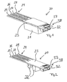
- Fig. 1 and 2 show a preferred embodiment of a splitter device 20 according to the invention, wherein the splitter device 20 according to Fig. 1 and 2 is designed as a single plug or as a single splitter.
- Fig. 1 shows the splitter device 20 together with a housing 21, which is arranged around the active and / or passive components 22 for forming the actual splitter.
- the housing 21 is removed, so that the view of the active and / or passive components 22 of the actual splitter is released.
- the splitter device 20 includes a board 23. At a first end 24 of the board 23 a total of four contact tongues 25, 26, 27 and 28 are formed in the illustrated embodiment. Each of these contact tongues 25, 26, 27 and 28 provides two connection options or contact options, a first contact option on the top and a second possibility of contact on the underside of the respective contact tongue 25, 26, 27 and 28. With the four contact tongues 25, 26, 27 and 28, a total of eight connection options are thus provided.
- connection options Two of these connection options are used for contacting the so-called a-wire and b-wire of the high-frequency data signal (DATA / DSLAM), two connection options are used to make contact with the a-wire and b-wire of the low-pitched voice signal or voice signal (VOICE / POTS / ISDN) , two further connection options are used for contacting a-wire and b-wire of the combined voice data signal (LINE) and the other two connection options serve to provide a ground potential or ground potential (SHIELD).
- a-wires of the high-frequency data signal, the low-pitched voice signal and the combined voice-data signal are also referred to as "tip" and the b-wire as "ring”. In principle, it would be sufficient to provide the splitter device 20 with seven connection possibilities or contact possibilities, since the ground potential or ground potential of the splitter device 20 only needs to be made available once.
- the splitter device 20 designed as a single splitter can be inserted from the front into a functional element, designed as a separating element or switching element, of a distributor strip of a distributor device.
- 3 and 4 show a distributor block 29 formed as a distribution device of a telecommunications system in which a plurality of distribution strips 30 are arranged one above the other superimposed.
- a plurality of functional elements dividing elements or switching elements
- cutting clamps 31 are arranged on a front side of the distribution bar 30, and pass in the interior of the distribution bar in not shown contact springs of the functional elements.
- the splitter device 20 is according to 3 and 4 can be inserted from the front into a functional element of a distribution strip 30, wherein the contact tongues 25, 26, 27 and 28 contact the contact springs in the interior of the respective functional element after inserting the splitter device 20 into a functional element.
- a signal tapping means 32 is integrated into the splitter device 20.
- the signal tap means 32 which in the embodiment according to Fig. 1 and 2 is formed as a socket of a plug-in connection, the voltage applied to the splitter device 20 and to the components 22 of the splitter signals or telecommunications services can be tapped and fed to a non-illustrated evaluation, without having to pull the splitter device 20 from the functional element. Accordingly, it is also possible to access the contact springs of the corresponding functional element via the signal tapping means 32 even when the splitter device 20 is inserted in a functional element. In order for measurements and test and test operations in the case of inserted from the front into a functional element splitter device 20 and thus during operation of the splitter device 20 is possible.
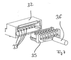
- Fig. 6 shows the trained as a socket of a connector Signalabgriffsstoff 32 of the splitter device 20 in solo view.
- a total of eight contact pins 33 are integrated into the signal pickup means 32, wherein the signals applied to the contact tongues 25, 26, 27 and 28 can be picked off at the contact pins 33.
- Fig. 6 shown opposite the contact pins 33 by 90 ° angled terminals 34 serve the connection of the signal pick-off means 32 on the board 23 of the splitter device 20 and the contacting of corresponding, integrated circuit board 23 in the interconnects, at which the contact tongues 25, 26, 27 and 28 applied signals can be tapped.
- a suitably trained plug 35 can be inserted.
- Fig. 7 shows a connector 35 in conjunction with the signal pick-off means 32, wherein the signals applied to the contact pins 33 or signals can be transmitted to an evaluation using the acting on the plug 35 cable 36 ultimately.
- a switching means 37 is integrated in the splitter device 20 in addition to the signal pick-off means 32.
- the switching means 37 like the signal pick-off means 32, are associated with an end 38, opposite the end 24, of the board 23.
- By means of the switching means 37 are applied to the splitter device 20 and the splitter signals selectively switched on and / or off and / or switched. This makes it possible to influence the access to the signals applied to the splitter device 20 for testing purposes or measurement purposes. It is possible to switch through one or more services, to connect one or more services to at least one other service and to switch off one or more services. In this way, the services provided at the contact tongues 25, 26, 27 and 28 for test purposes and measurement purposes can be combined with one another almost arbitrarily and provided in an appropriate combination at the signal tapping means 32. This will be discussed in greater detail below.
- the switching means 37 is designed as a so-called DIP switch.
- Fig. 5 shows the trained as a DIP switch switching means 37 in solo representation. So, the DIP switch has according to Fig. 5 over a total of eight individual switches 39, wherein each of the individual switches 39 can be opened or closed by itself. In Fig. 5 all individual switches 39 are shown in the so-called ON position, ie closed. About contact feet 40 designed as a DIP switch switching means 37 to the corresponding conductor tracks of the board 23 can be connected.
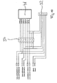
- Fig. 8 shows a first possibility for internal connection of the splitter device 20 according to FIG Fig. 1 and 2 integrated switching means 37 with a provided by the components 22 of the splitter device 20 splitter 41 and also integrated into the splitter device 20 Signalabgriffsstoff 32nd
- Fig. 8 In the wiring option according to Fig. 8 are at the inputs of the switches 1 and 2 of the switching means 37, the a-wire (Tip) and the b-wire (ring) of low-frequency speech signal (VOICE / POTS / ISDN). Outputs of the switches 1 and 2 with these signals are supplied to the splitter 41. The outputs of the switches 1 and 2 with the a-wire and b-wire of the low-frequency speech signal are according to Fig. 8 Further connected to the two first contact pins 33 of the signal pick-off means 32 seen from the left. The same procedure applies to the a-wire and the b-wire of the high-frequency data signal (DSLAM / DATA).
- the a-wire and the b-wire of the high-frequency data signal are fed to the inputs of the switches 3 and 4. At the outputs of the switches 3 and 4 of the switching means 37, these signals are kept ready and supplied on the one hand the splitter 41 as input signals and on the other hand seen from the left fifth and sixth contact pins 33 of the signal pickup means 32.
- the splitter 41 generates from the low-frequency speech signal (VOICE / POTS / ISDN) and the high-frequency data signal (DSLAM / DATA) a combined voice data signal (LINE), this LI-NE signal on the one hand inputs of the switches 5 and 6 of the switching means 37th and on the other hand, directly to the third and fourth contact pins 33 of the signal pickup means 32 as seen from the left.
- the ground potential (ground) (SHIELD) is applied to the two remaining contact pins 33 of the signal pickup means.
- Fig. 9 shows another internal Verschaltungsschkeit. So is in the Verschaltungsssenkeit according to Fig. 9 the a-wire and the b-wire of the low-frequency speech signal (VOICE / POTS / ISDN) are applied on the one hand to the inputs of the switches 1 and 2 of the switching means 37 and on the other hand directly to the two first contact pins 33 of the signal pick-off means 32 seen from the left.
- the a-wire and the b-wire of the high-frequency data signal (DSLAM / DATA) are applied on the one hand to the inputs of the switches 3 and 4 of the switching means 37 and on the other hand directly to the fifth and sixth contact pins 33 of the signal pick-off means 32 seen from the left.
- DLAM / DATA high-frequency data signal
- the conductors of low-frequency speech signal and high-frequency data signal applied to the inputs of the switches 1 to 4 are supplied as an input signal to the splitter 41, which generates a combined voice and data signal (LINE) from this.
- LINE combined voice and data signal
- This is applied to inputs of the switches 5 and 6 of the switching means 37, wherein after passing through the switches 5 and 6, the combined voice and data signal to the seen from the left third and fourth contact pins 33 of the signal pickup means 32 is applied.
- the ground potential (ground) (SHIELD) is in turn applied to the two remaining contact pins 33 of the signal tapping means 32.
- FIG. 12 shows another internal interconnection capability of splitter 41, switching means 37 and signal tapping means 32.
- FIGS Fig. 10 for the switching means 37 and the signal pick-up means 32 simplified equivalent circuit diagrams chosen.
- the peculiarity of Verschaltungsitz according to Fig. 10 results from the wiring of the switches 7 and 8 of the switching means 37, wherein the inputs of the switches 7 and 8 on the one hand a-wire and b-wire of the high-frequency data signal (DATA / DSLAM) and to the outputs of the switches 7 and 8 a- Core and b-wire of the combined voice and data signal (LINE) are connected.
- DATA / DSLAM high-frequency data signal
- LINE combined voice and data signal
- the splitter device 20 is used as a "switching module" in such a way that the low-frequency speech signals can be switched off and thus the high-frequency data signals are available directly at the LINE connection.
- a splitter-based asymmetric transmission to a symmetric transmission (eg SDSL) (pure data operation).
- a symmetric transmission eg SDSL
- this method is that neither a so-called "jumper cable” from the data port to the Linean gleich must be laid, nor that the voice signal is disconnected at the Voiceanschluß must become. The latter would cause interference, for example, in the symmetric transmission.
- Fig. 11 to 14 show further embodiments according to the invention of splitter devices in the sense of the present invention.
- Splitter devices shown up to 15 differ from the splitter device according to FIG Fig. 1 and 2 by the specific configuration of the signal tapping means integrated in the splitter devices as well as switching means or by the fact that no switching means is integrated into the splitter device. Otherwise, the splitter facilities are in accordance with Fig. 11 to 14 however, with the splitter device 20 according to FIG Fig. 1 to 2 match. For identical assemblies, therefore, like reference numerals are used to avoid unnecessary repetition.
- a switching means 37 and a Signalabgriffsstoff 32 integrated therein In contrast to the embodiment according to Fig. 1 and 2 is according to the splitter device 42 Fig. 12 the Signalabgriffsstoff 32 is not formed as a socket of a plug device, but rather as a band of juxtaposed contact pads.
- the switching means 37 is not designed as a DIP switch, but as a so-called push-button switch.
- the button switch can have two or more switching positions.
- splitter 42 can be as well as with the splitter device 20 according to Fig. 1 and 2 selectively influence individual services or signals, namely either switching on or off or also switching through. The services or signals can be read out at the signal tapping means 32 and fed to a non-illustrated evaluation device for test purposes or for checks.
- Fig. 12 shows a splitter device 43 with integrated into the splitter device 43
- Signalabgriffsmittein 32 which in the embodiment of the Fig. 12 are formed as vias, in the for reading the signals, for example a measuring tip of a measuring instrument can be inserted.
- the arranged between the two vias hole 44 serves to grasp the splitter device 43 for facilitating pulling them out of a functional element of a distribution strip of a manifold block.
- Fig. 13 essentially corresponds to the embodiment according to Fig. 12 However, in the embodiment of the Fig. 13 a total of eight vias in the board 23 of the splitter device 45 are integrated. A likewise integrated into the board 23 hole 44 in turn serves to facilitate gripping the splitter device 45 when pulling them out of a functional element.
- Fig. 12 and 13 shown embodiments of a splitter device 43 and 45, no switching means for selectively connecting, switching off or switching through individual services or signals are shown.
- the splitter devices 43 and 45 according to Fig. 12 and 13 To provide designed as a DIP switch or button switch switching means.
- Den as DIP switches according to the embodiment according to Fig. 1 and 2 and the as push-button switches according to the embodiment according to Fig. 11 trained switching means 37 has in common that they can be actuated by an operator who influences the switching position of the switching means 37 on site.
- the switching means 37 as remotely controllable switching means and to integrate them into the housing 21 together with the assemblies 22 which form the splitter 41 of the splitter device.
- Such remote-controllable switching means may be, for example, relays, wherein the switching position of the relay can be influenced by control signals that are transmitted via the same copper pair, such as the high-frequency data signals and low-frequency speech signals.
- the control signals for the remote-controlled relays are superimposed in the modulation process the data signals or the speech signals.
- the control signals may, for example, be voltage pulses with the aid of which the remote-controlled relays can be opened or closed.
- An embodiment of the switching means as remotely controllable switching means has the advantage that to carry out test and test operations no operator must make any more on site influencing the splitter devices. Rather, this can be done from any location.
- Fig. 14 shows a further embodiment of a splitter device 46 according to the invention.
- a signal pick-off means 32 is integrated into the splitter device, wherein the signal pick-off means 32 is embodied in RJ plug technology.
- RJ plug technology for example, an RJ11 or RJ45 plug can be used.
- remotely controllable switching means can be integrated in the housing 21.
- splitter devices are therefore proposed, in which signal tapping means are integrated.
- signals or telecommunication services present at the splitter device can also be read out when the splitter device is inserted from the front into a functional element or into the contact springs of the functional element.
- Such a splitter device therefore no longer has to be pulled out of the functional element in order to read the signals and to carry out test and test procedures. Test and test procedures can also be carried out during operation of the splitter device.
- Particularly preferred is an embodiment in which in addition to the Signalabgriffsmitteln switching means are integrated into the splitter device. Using the switching means individual services can be switched on, switched off or switched through. In combination with the signal tapping means, access to signals influenced or not influenced by the switching means is then ensured.
Landscapes
- Engineering & Computer Science (AREA)
- Computer Networks & Wireless Communication (AREA)
- Structure Of Telephone Exchanges (AREA)
- Details Of Connecting Devices For Male And Female Coupling (AREA)
- Two-Way Televisions, Distribution Of Moving Picture Or The Like (AREA)
- Details Of Television Systems (AREA)
- Cigarettes, Filters, And Manufacturing Of Filters (AREA)
- Cable Transmission Systems, Equalization Of Radio And Reduction Of Echo (AREA)
Claims (7)
- Dispositif de séparation pour un répartiteur d'un équipement de télécommunication, le dispositif de séparation présentant au moins un séparateur (41) et pouvant être inséré dans le répartiteur et au moins un moyen de prélèvement de signal (32) étant intégré dans le dispositif de séparation afin de prélever les signaux présents sur le ou sur chaque séparateur (41), caractérisé en ce qu'au moins un moyen de commutation (37) est en plus intégré dans le dispositif de séparation pour connecter et/ou déconnecter et/ou transférer les signaux présents sur le ou sur chaque séparateur.
- Dispositif de séparation selon la revendication 1, caractérisé en ce que le ou chaque moyen de commutation (37) est configuré pour pouvoir être commandé à distance.
- Dispositif de séparation selon la revendication 1 ou 2, caractérisé en ce que celui-ci peut être inséré dans au moins un élément fonctionnel d'une barrette de répartition (30) du répartiteur, un séparateur étant alors intégré dans le dispositif de séparation pour chaque élément fonctionnel lorsque celui-ci peut être inséré dans plusieurs éléments fonctionnels.
- Dispositif de séparation selon la revendication 3, caractérisé en ce que lorsque celui-ci peut être inséré dans plusieurs éléments fonctionnels, un moyen de prélèvement de signal est alors intégré dans le dispositif de séparation pour chaque élément fonctionnel.
- Dispositif de séparation selon la revendication 3 ou 4, caractérisé en ce que celui-ci peut être inséré de préférence par l'avant avec des languettes de contact (25, 26, 27, 28) entre les ressorts de contact d'au moins un élément fonctionnel de la barrette de répartition (30).
- Dispositif de séparation selon l'une ou plusieurs des revendications 1 à 5, caractérisé en ce que les signaux présents sur le ou sur chaque séparateur peuvent être prélevés à l'aide du ou de chaque moyen de prélèvement de signal (32) lorsque le dispositif de séparation est inséré par l'avant dans le répartiteur.
- Dispositif de séparation selon l'une ou plusieurs des revendications 1 à 6, caractérisé en ce que celui-ci peut être inséré par l'avant dans au moins un élément fonctionnel d'une barrette de répartition (30) du répartiteur.
Applications Claiming Priority (2)
| Application Number | Priority Date | Filing Date | Title |
|---|---|---|---|
| DE20315191U DE20315191U1 (de) | 2003-09-30 | 2003-09-30 | Splittereinrichtung für eine Verteilereinrichtung einer Telekommunikationsanlage |
| PCT/EP2004/010828 WO2005034533A1 (fr) | 2003-09-30 | 2004-09-28 | Dispositif de separation pour systeme de distribution d'une installation de telecommunication |
Publications (2)
| Publication Number | Publication Date |
|---|---|
| EP1668926A1 EP1668926A1 (fr) | 2006-06-14 |
| EP1668926B1 true EP1668926B1 (fr) | 2010-04-07 |
Family
ID=29724281
Family Applications (1)
| Application Number | Title | Priority Date | Filing Date |
|---|---|---|---|
| EP04787030A Expired - Lifetime EP1668926B1 (fr) | 2003-09-30 | 2004-09-28 | Dispositif de separation pour systeme de distribution d'une installation de telecommunication |
Country Status (4)
| Country | Link |
|---|---|
| EP (1) | EP1668926B1 (fr) |
| AT (1) | ATE463930T1 (fr) |
| DE (2) | DE20315191U1 (fr) |
| WO (1) | WO2005034533A1 (fr) |
Families Citing this family (4)
| Publication number | Priority date | Publication date | Assignee | Title |
|---|---|---|---|---|
| EP1804524A1 (fr) * | 2005-12-29 | 2007-07-04 | 3M Innovative Properties Company | Ensemble de télécommunication comprenant au moins un module de télécommunication, un bus de test et un jeu d'éléments |
| DE102008045337B4 (de) * | 2008-09-01 | 2010-10-21 | Adc Gmbh | Verteileranschlussmodul |
| CN202135122U (zh) * | 2011-05-20 | 2012-02-01 | 泰科电子(上海)有限公司 | 信号分离器和信号分离器组件 |
| DE102018102176A1 (de) * | 2018-01-31 | 2019-08-01 | Cobinet Fernmelde- Und Datennetzkomponenten Gmbh | Splitter, Verbindungsmodul mit Splitter sowie Kabelverzweiger und Verwendung eines Splitters |
Family Cites Families (2)
| Publication number | Priority date | Publication date | Assignee | Title |
|---|---|---|---|---|
| DE10029870A1 (de) * | 2000-06-16 | 2002-01-03 | Rxs Kabelgarnituren Gmbh & Co | Verteilereinrichtung einer Datensignal-Verarbeitungsanlage und Datensignal-Verarbeitungsanlage |
| PL369219A1 (en) * | 2002-10-03 | 2005-04-18 | Tyco Electronics Raychem Sa | Filter systems for broadband telecommunication facilities |
-
2003
- 2003-09-30 DE DE20315191U patent/DE20315191U1/de not_active Expired - Lifetime
-
2004
- 2004-09-28 AT AT04787030T patent/ATE463930T1/de not_active IP Right Cessation
- 2004-09-28 WO PCT/EP2004/010828 patent/WO2005034533A1/fr not_active Ceased
- 2004-09-28 EP EP04787030A patent/EP1668926B1/fr not_active Expired - Lifetime
- 2004-09-28 DE DE502004011002T patent/DE502004011002D1/de not_active Expired - Lifetime
Also Published As
| Publication number | Publication date |
|---|---|
| EP1668926A1 (fr) | 2006-06-14 |
| DE502004011002D1 (de) | 2010-05-20 |
| WO2005034533A1 (fr) | 2005-04-14 |
| ATE463930T1 (de) | 2010-04-15 |
| DE20315191U1 (de) | 2003-12-04 |
Similar Documents
| Publication | Publication Date | Title |
|---|---|---|
| EP1290762B1 (fr) | Module distributeur a connexions utilise en telecommunications et dans des systemes de donnees | |
| DE69121060T2 (de) | Digitales Verteilungsgerät | |
| DE69410269T2 (de) | Rückwärtiges dsx verbindungssystem | |
| DE4121836C2 (de) | Reihenklemme mit Aufsteckmodul | |
| EP1527503B1 (fr) | Module de connexion de dispositif de distribution utilise en technique de telecommunication et de traitement de donnees | |
| EP1668926B1 (fr) | Dispositif de separation pour systeme de distribution d'une installation de telecommunication | |
| DE102005022547B4 (de) | Verteilereinrichtung im Teilnehmeranschlussbereich | |
| DE20203911U1 (de) | Kontaktfeld, Messanordnung mit einem Kontaktfeld und Anschluss-, Trenn- oder Zusatzmodul der Telekommunikationstechnik mit einem Kontaktfeld oder einer Messanordnung | |
| DE19751699C2 (de) | Vorrichtung zum Verbinden von Kabeladern | |
| DE102005022689B4 (de) | Aktive Verteilereinrichtung im Teilnehmeranschlussbereich | |
| DE602004012277T2 (de) | Benutzeranschluss-Testvorrichtung und Breitband- und Schmalband-Kommunikationssystem | |
| EP1929794A1 (fr) | Module de connexion a fonctions integrees | |
| DE4042240A1 (de) | Anschlussmodul fuer eine verteilereinrichtung, insbesondere fuer den hauptverteiler von fernmeldeeinrichtungen | |
| DE102008031521B3 (de) | Systemarchitektur und Verfahren zur Anbindung eines MSAN an einen Hauptverteiler und Verteileranschlussmodul | |
| DE602004007477T2 (de) | Modulare Anordnung im Gebiet der Telekommunikation | |
| DE60202056T2 (de) | Verbindungsvorrichtung | |
| EP2201786B1 (fr) | Dispositif répartiteur d'une installation de télécommunication, et connecteur pour un dispositif répartiteur d'une installation de télécommunication | |
| EP1304579B1 (fr) | Appareil pour tester des conducteurs électriques | |
| EP2057717B1 (fr) | Dispositif de répartition d'une installation de télécommunication, dispositif de réception d'un tel dispositif de répartition ainsi que fiche de connexion | |
| DE10336020B4 (de) | Prüfsystem und Verfahren zur zentralen Durchführung von Prüfungen der Teilnehmeranschlussleitungen in einem Telekommunikationsnetz | |
| DE10261927B4 (de) | Flachkabel-System | |
| EP2002665B1 (fr) | Dispositif répartiteur d'une installation de télécommunication, pourvu d'un dispositif de compensation | |
| DE19523941C1 (de) | Schnittstellenschaltung zum Anschließen eines elektrischen Geräts an einen Bus | |
| DE202009015835U1 (de) | Schutzeinrichtung einer Verteilereinrichtung | |
| DE102010007856A1 (de) | Verfahren und Trennleiste zum alternativen Verbinden einer mit einer ersten Eingangsleitung verbundenen Ausgangsleitung mit einer zweiten Eingangsleitung |
Legal Events
| Date | Code | Title | Description |
|---|---|---|---|
| PUAI | Public reference made under article 153(3) epc to a published international application that has entered the european phase |
Free format text: ORIGINAL CODE: 0009012 |
|
| 17P | Request for examination filed |
Effective date: 20050708 |
|
| AK | Designated contracting states |
Kind code of ref document: A1 Designated state(s): AT BE BG CH CY CZ DE DK EE ES FI FR GB GR HU IE IT LI LU MC NL PL PT RO SE SI SK TR |
|
| DAX | Request for extension of the european patent (deleted) | ||
| RIN1 | Information on inventor provided before grant (corrected) |
Inventor name: LIPKOWSKI, MARC Inventor name: HOFFMANN, WOLFGANG Inventor name: VOGT, RAINER |
|
| 17Q | First examination report despatched |
Effective date: 20090320 |
|
| GRAP | Despatch of communication of intention to grant a patent |
Free format text: ORIGINAL CODE: EPIDOSNIGR1 |
|
| GRAS | Grant fee paid |
Free format text: ORIGINAL CODE: EPIDOSNIGR3 |
|
| GRAA | (expected) grant |
Free format text: ORIGINAL CODE: 0009210 |
|
| AK | Designated contracting states |
Kind code of ref document: B1 Designated state(s): AT BE BG CH CY CZ DE DK EE ES FI FR GB GR HU IE IT LI LU MC NL PL PT RO SE SI SK TR |
|
| REG | Reference to a national code |
Ref country code: GB Ref legal event code: FG4D Free format text: NOT ENGLISH |
|
| REG | Reference to a national code |
Ref country code: CH Ref legal event code: EP |
|
| REG | Reference to a national code |
Ref country code: IE Ref legal event code: FG4D Free format text: LANGUAGE OF EP DOCUMENT: GERMAN |
|
| REF | Corresponds to: |
Ref document number: 502004011002 Country of ref document: DE Date of ref document: 20100520 Kind code of ref document: P |
|
| REG | Reference to a national code |
Ref country code: NL Ref legal event code: VDEP Effective date: 20100407 |
|
| PG25 | Lapsed in a contracting state [announced via postgrant information from national office to epo] |
Ref country code: SI Free format text: LAPSE BECAUSE OF FAILURE TO SUBMIT A TRANSLATION OF THE DESCRIPTION OR TO PAY THE FEE WITHIN THE PRESCRIBED TIME-LIMIT Effective date: 20100407 |
|
| REG | Reference to a national code |
Ref country code: IE Ref legal event code: FD4D |
|
| PG25 | Lapsed in a contracting state [announced via postgrant information from national office to epo] |
Ref country code: NL Free format text: LAPSE BECAUSE OF FAILURE TO SUBMIT A TRANSLATION OF THE DESCRIPTION OR TO PAY THE FEE WITHIN THE PRESCRIBED TIME-LIMIT Effective date: 20100407 Ref country code: ES Free format text: LAPSE BECAUSE OF FAILURE TO SUBMIT A TRANSLATION OF THE DESCRIPTION OR TO PAY THE FEE WITHIN THE PRESCRIBED TIME-LIMIT Effective date: 20100718 Ref country code: SE Free format text: LAPSE BECAUSE OF FAILURE TO SUBMIT A TRANSLATION OF THE DESCRIPTION OR TO PAY THE FEE WITHIN THE PRESCRIBED TIME-LIMIT Effective date: 20100407 |
|
| PG25 | Lapsed in a contracting state [announced via postgrant information from national office to epo] |
Ref country code: FI Free format text: LAPSE BECAUSE OF FAILURE TO SUBMIT A TRANSLATION OF THE DESCRIPTION OR TO PAY THE FEE WITHIN THE PRESCRIBED TIME-LIMIT Effective date: 20100407 |
|
| PG25 | Lapsed in a contracting state [announced via postgrant information from national office to epo] |
Ref country code: PL Free format text: LAPSE BECAUSE OF FAILURE TO SUBMIT A TRANSLATION OF THE DESCRIPTION OR TO PAY THE FEE WITHIN THE PRESCRIBED TIME-LIMIT Effective date: 20100407 Ref country code: GR Free format text: LAPSE BECAUSE OF FAILURE TO SUBMIT A TRANSLATION OF THE DESCRIPTION OR TO PAY THE FEE WITHIN THE PRESCRIBED TIME-LIMIT Effective date: 20100708 Ref country code: CY Free format text: LAPSE BECAUSE OF FAILURE TO SUBMIT A TRANSLATION OF THE DESCRIPTION OR TO PAY THE FEE WITHIN THE PRESCRIBED TIME-LIMIT Effective date: 20100428 |
|
| PG25 | Lapsed in a contracting state [announced via postgrant information from national office to epo] |
Ref country code: DK Free format text: LAPSE BECAUSE OF FAILURE TO SUBMIT A TRANSLATION OF THE DESCRIPTION OR TO PAY THE FEE WITHIN THE PRESCRIBED TIME-LIMIT Effective date: 20100407 Ref country code: IE Free format text: LAPSE BECAUSE OF FAILURE TO SUBMIT A TRANSLATION OF THE DESCRIPTION OR TO PAY THE FEE WITHIN THE PRESCRIBED TIME-LIMIT Effective date: 20100407 Ref country code: EE Free format text: LAPSE BECAUSE OF FAILURE TO SUBMIT A TRANSLATION OF THE DESCRIPTION OR TO PAY THE FEE WITHIN THE PRESCRIBED TIME-LIMIT Effective date: 20100407 |
|
| PLBE | No opposition filed within time limit |
Free format text: ORIGINAL CODE: 0009261 |
|
| STAA | Information on the status of an ep patent application or granted ep patent |
Free format text: STATUS: NO OPPOSITION FILED WITHIN TIME LIMIT |
|
| PG25 | Lapsed in a contracting state [announced via postgrant information from national office to epo] |
Ref country code: SK Free format text: LAPSE BECAUSE OF FAILURE TO SUBMIT A TRANSLATION OF THE DESCRIPTION OR TO PAY THE FEE WITHIN THE PRESCRIBED TIME-LIMIT Effective date: 20100407 Ref country code: RO Free format text: LAPSE BECAUSE OF FAILURE TO SUBMIT A TRANSLATION OF THE DESCRIPTION OR TO PAY THE FEE WITHIN THE PRESCRIBED TIME-LIMIT Effective date: 20100407 |
|
| 26N | No opposition filed |
Effective date: 20110110 |
|
| BERE | Be: lapsed |
Owner name: CCS TECHNOLOGY, INC. Effective date: 20100930 |
|
| PG25 | Lapsed in a contracting state [announced via postgrant information from national office to epo] |
Ref country code: IT Free format text: LAPSE BECAUSE OF FAILURE TO SUBMIT A TRANSLATION OF THE DESCRIPTION OR TO PAY THE FEE WITHIN THE PRESCRIBED TIME-LIMIT Effective date: 20100407 |
|
| PG25 | Lapsed in a contracting state [announced via postgrant information from national office to epo] |
Ref country code: MC Free format text: LAPSE BECAUSE OF NON-PAYMENT OF DUE FEES Effective date: 20100930 |
|
| GBPC | Gb: european patent ceased through non-payment of renewal fee |
Effective date: 20100928 |
|
| PG25 | Lapsed in a contracting state [announced via postgrant information from national office to epo] |
Ref country code: BE Free format text: LAPSE BECAUSE OF NON-PAYMENT OF DUE FEES Effective date: 20100930 |
|
| PG25 | Lapsed in a contracting state [announced via postgrant information from national office to epo] |
Ref country code: GB Free format text: LAPSE BECAUSE OF NON-PAYMENT OF DUE FEES Effective date: 20100928 |
|
| PG25 | Lapsed in a contracting state [announced via postgrant information from national office to epo] |
Ref country code: AT Free format text: LAPSE BECAUSE OF NON-PAYMENT OF DUE FEES Effective date: 20100928 |
|
| PG25 | Lapsed in a contracting state [announced via postgrant information from national office to epo] |
Ref country code: BG Free format text: LAPSE BECAUSE OF FAILURE TO SUBMIT A TRANSLATION OF THE DESCRIPTION OR TO PAY THE FEE WITHIN THE PRESCRIBED TIME-LIMIT Effective date: 20100407 Ref country code: LU Free format text: LAPSE BECAUSE OF NON-PAYMENT OF DUE FEES Effective date: 20100928 Ref country code: HU Free format text: LAPSE BECAUSE OF FAILURE TO SUBMIT A TRANSLATION OF THE DESCRIPTION OR TO PAY THE FEE WITHIN THE PRESCRIBED TIME-LIMIT Effective date: 20101008 |
|
| PG25 | Lapsed in a contracting state [announced via postgrant information from national office to epo] |
Ref country code: TR Free format text: LAPSE BECAUSE OF FAILURE TO SUBMIT A TRANSLATION OF THE DESCRIPTION OR TO PAY THE FEE WITHIN THE PRESCRIBED TIME-LIMIT Effective date: 20100407 |
|
| PG25 | Lapsed in a contracting state [announced via postgrant information from national office to epo] |
Ref country code: PT Free format text: LAPSE BECAUSE OF NON-PAYMENT OF DUE FEES Effective date: 20100407 |
|
| PG25 | Lapsed in a contracting state [announced via postgrant information from national office to epo] |
Ref country code: BG Free format text: LAPSE BECAUSE OF FAILURE TO SUBMIT A TRANSLATION OF THE DESCRIPTION OR TO PAY THE FEE WITHIN THE PRESCRIBED TIME-LIMIT Effective date: 20100707 |
|
| REG | Reference to a national code |
Ref country code: FR Ref legal event code: PLFP Year of fee payment: 12 |
|
| PGFP | Annual fee paid to national office [announced via postgrant information from national office to epo] |
Ref country code: CH Payment date: 20150928 Year of fee payment: 12 |
|
| REG | Reference to a national code |
Ref country code: FR Ref legal event code: PLFP Year of fee payment: 13 |
|
| REG | Reference to a national code |
Ref country code: CH Ref legal event code: PL |
|
| PG25 | Lapsed in a contracting state [announced via postgrant information from national office to epo] |
Ref country code: CH Free format text: LAPSE BECAUSE OF NON-PAYMENT OF DUE FEES Effective date: 20160930 Ref country code: LI Free format text: LAPSE BECAUSE OF NON-PAYMENT OF DUE FEES Effective date: 20160930 |
|
| REG | Reference to a national code |
Ref country code: FR Ref legal event code: PLFP Year of fee payment: 14 |
|
| PGFP | Annual fee paid to national office [announced via postgrant information from national office to epo] |
Ref country code: FR Payment date: 20170925 Year of fee payment: 14 Ref country code: CZ Payment date: 20170920 Year of fee payment: 14 |
|
| PGFP | Annual fee paid to national office [announced via postgrant information from national office to epo] |
Ref country code: DE Payment date: 20170927 Year of fee payment: 14 |
|
| REG | Reference to a national code |
Ref country code: DE Ref legal event code: R119 Ref document number: 502004011002 Country of ref document: DE |
|
| PG25 | Lapsed in a contracting state [announced via postgrant information from national office to epo] |
Ref country code: CZ Free format text: LAPSE BECAUSE OF NON-PAYMENT OF DUE FEES Effective date: 20180928 |
|
| PG25 | Lapsed in a contracting state [announced via postgrant information from national office to epo] |
Ref country code: DE Free format text: LAPSE BECAUSE OF NON-PAYMENT OF DUE FEES Effective date: 20190402 |
|
| PG25 | Lapsed in a contracting state [announced via postgrant information from national office to epo] |
Ref country code: FR Free format text: LAPSE BECAUSE OF NON-PAYMENT OF DUE FEES Effective date: 20180930 |