EP1684188A2 - Système et appareil électronique de transfert de données - Google Patents
Système et appareil électronique de transfert de données Download PDFInfo
- Publication number
- EP1684188A2 EP1684188A2 EP06250258A EP06250258A EP1684188A2 EP 1684188 A2 EP1684188 A2 EP 1684188A2 EP 06250258 A EP06250258 A EP 06250258A EP 06250258 A EP06250258 A EP 06250258A EP 1684188 A2 EP1684188 A2 EP 1684188A2
- Authority
- EP
- European Patent Office
- Prior art keywords
- data
- link state
- data transferring
- pci express
- link
- Prior art date
- Legal status (The legal status is an assumption and is not a legal conclusion. Google has not performed a legal analysis and makes no representation as to the accuracy of the status listed.)
- Granted
Links
Images


Classifications
-
- G—PHYSICS
- G06—COMPUTING OR CALCULATING; COUNTING
- G06F—ELECTRIC DIGITAL DATA PROCESSING
- G06F13/00—Interconnection of, or transfer of information or other signals between, memories, input/output devices or central processing units
- G06F13/38—Information transfer, e.g. on bus
- G06F13/42—Bus transfer protocol, e.g. handshake; Synchronisation
- G06F13/4282—Bus transfer protocol, e.g. handshake; Synchronisation on a serial bus, e.g. I2C bus, SPI bus
- G06F13/4291—Bus transfer protocol, e.g. handshake; Synchronisation on a serial bus, e.g. I2C bus, SPI bus using a clocked protocol
-
- Y—GENERAL TAGGING OF NEW TECHNOLOGICAL DEVELOPMENTS; GENERAL TAGGING OF CROSS-SECTIONAL TECHNOLOGIES SPANNING OVER SEVERAL SECTIONS OF THE IPC; TECHNICAL SUBJECTS COVERED BY FORMER USPC CROSS-REFERENCE ART COLLECTIONS [XRACs] AND DIGESTS
- Y02—TECHNOLOGIES OR APPLICATIONS FOR MITIGATION OR ADAPTATION AGAINST CLIMATE CHANGE
- Y02D—CLIMATE CHANGE MITIGATION TECHNOLOGIES IN INFORMATION AND COMMUNICATION TECHNOLOGIES [ICT], I.E. INFORMATION AND COMMUNICATION TECHNOLOGIES AIMING AT THE REDUCTION OF THEIR OWN ENERGY USE
- Y02D10/00—Energy efficient computing, e.g. low power processors, power management or thermal management
Definitions
- the present invention generally relates to a data transferring system that transfers data and an electronic apparatus that provides the data transferring system.
- PCI Express peripheral component interconnect express, registered trademark
- link states of L0, L0s, L1, and L2 are defined.
- the link state L0 is a normal mode and the power consumption is lowered corresponding to the change of the link state from L0s to L2. Details of the link states are explained below.
- Fig. 15 is a timing chart showing a control example of power source management by the link states.
- a power saving mode is established in a ms order and power source management is executed by software control, and the period of the power saving mode is shown in "L2".
- the power saving mode is established in a ⁇ s order and the power source management is executed by hardware control, and the period of the power saving mode is shown in "L1”.
- the power saving mode is established in a ns order and the power source management is executed by hardware control, and the period of the power saving mode is shown in "LOs".
- a data transferring system and an electronic apparatus providing the data transferring system in which larger power saving can be executed compared with a conventional system in image data transfer based on the PCI Express standard.
- a data transferring system that transfers image data based on the PCI Express standard by synchronizing with a line synchronizing signal or a frame synchronizing signal.
- the data transferring system includes a packet gathering unit that transfers the image data (packets) by causing a period between the packets to be transferred in one cycle of the synchronizing signal to be shorter than a time that is required to transit from a link state L0 to a link state L0s and from the link state L0s to the link state L0.
- a data transferring system that provides a plurality of data transferring devices each of which transfers image data based on the PCI Express standard by synchronizing with a line synchronizing signal or a frame synchronizing signal and that transfers a plurality of image data from the plural data transferring devices in parallel.
- the data transferring system includes a packet gathering unit that makes the image data (packets) to be transferred by one of the data transferring devices a transfer reference, delays transferring time of the image data of the other data transferring devices to be transferred before transferring the image data of the transfer reference, and makes a period between the packets to be transferred from the data transferring devices to be shorter than a time that is required to transit from a link state L0 to a link state L0s and from the link state L0s to the link state L0.
- transit periods from a link state L0 to a link state L0s and from the link state L0s to the link state L0 are reduced and the period of the link state L0s is increased. Therefore, the power saving can be realized compared with the conventional system.
- the embodiment of the present invention utilizes PCI Express being one of the high speed serial buses, and as a premise of the embodiment of the present invention, the outline of the PCI Express Standard is explained by using an extract of Non-Patent Document 1.
- the high speed serial bus signifies an interface that can transmit data in a high speed (approximately over 100 Mbps) by serial transmission with the use of one transmission line.
- PCI Express is a bus standardized as a standard extended bus capable of being used in all computers as a successor to PCI, and has features, such as low voltage differential signal transmission, independent communication channels for reception and transmission in point to point, packetized split transaction, and high scalability depending on difference of link structures.
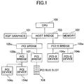
- Fig. 1 is a block diagram showing a configuration of an existing PCI system.
- Fig. 2 is a block diagram showing a configuration of a PCI Express system.
- a tree structure is formed.
- PCI-X devices 104a and 104b (of the upward compatibility standard of PCI) are connected to a host bridge 103, to which a CPU 100, an AGP graphics 101, and a memory 102 are connected, via a PCI-X bridge 105a.
- a PCI bridge 105b to which PCI devices 104c and 104d are connected and a PCI bridge 107 to which PCI bus slots 106 are connected are connected to the host bridge 103 via a PCI bridge 105c.
- a tree structure is also formed.
- a PCI Express graphics (port) 113 is connected to a root complex 112, to which a CPU 110 and a memory 111 are connected, by a PCI Express link 114a;
- a switch 117a to which an end point 115a and a legacy end point 116a are connected by PCI Express links 114b, is connected to the root complex 112 by a PCI Express link 114c;
- a switch 117b to which an end point 115b and a legacy end point 116b are connected by PCI Express links 114d, and a PCI bridge 119, to which PCI bus slots 118 are connected, are connected to a switch 117c by PCI Express links 114e; and the switch 117c is connected to the root complex 112 by a PCI Express link 114f.
- Fig. 3 is a block diagram showing a PCI Express platform in a desktop/a mobile computer.
- the PCI Express platform shown in Fig. 3 is an example which is assumed to be actually used.
- a CPU 121 is connected to a memory hub 124 (corresponding to a root complex), to which a memory 123 is connected, by a CPU host bus 122.
- a graphics (port) 125 is connected to the memory hub 124 by a PCI Express link 126a of ⁇ 16.
- An I/O hub 127 having a conversion function is connected to the memory hub 124 by a PCI Express link 126a.
- Storage 129 is connected to the I/O hub 127 by, for example, a serial ATA (serial AT attachment) 128.
- a local I/O 131 is connected to the I/O hub 127 by an LPC (low pin count) connector 130, and a USB 2.0 132 and PCI bus slots 133 are connected to the I/O hub 127.
- a switch 134 is connected to the I/O hub 127 by a PCI Express link 126c
- a mobile dock 135 is connected to the switch 134 by a PCI Express link 126d
- a gigabit Ethernet LAN 136 is connected to the switch 134 by a PCI Express link 126e
- an add-in card 137 is connected to the switch 134 by a PCI Express link 126f.
- PCI Express in the PCI Express system, conventional buses, such as a PCI bus, a PCI-X bus, and an AGP bus are replaced by the PCI Express buses, and bridges (not shown) are used to connect the existing PCI/PCI-X devices.
- the connections between chip sets are executed by PCI Express connections, and existing buses, such as an IEEE 1394 (not shown), the Serial ATA 128, and the USB 2.0 132 are connected to the PCI Express buses by the I/O hub 127.
- Ports are physically in the same semiconductor device and are a set of transmitters/receivers forming links and signify interfaces which connect components logically one to one (point to point).
- the transfer rate is, for example, 2.5 Gbps in one direction (for the future, 5 Gbps and 10 Gbps are assumed).
- a lane is a set of two pairs of differential signals of, for example, 0.8 V, and is composed of a pair of transmission side signals (2 pieces) and a pair of reception side signals (2 pieces).
- a link is a group of lanes connecting the two ports and a dual simplex communication bus between components (devices).
- Fig. 4 a case of ⁇ 4 link is shown.
- Fig. 5 is a schematic diagram showing a lane connection example between devices. As shown in Fig. 5, when the lane width N connecting devices A and B is variable, a scalable band width can be obtained.
- the root complex 112 (refer to Fig. 2) is located in the upper most position of the I/O structure and connects a CPU and a memory subsystem to I/Os. In many cases, as shown in Fig. 3, the root complex is described as a memory hub in a block diagram.
- the root complex 112 (the memory hub 124) has one or more PCI Express ports (root ports), and each PCI Express port forms an independent I/O layer domain. In Fig. 2, rectangles in the root complex 112 are the PCI Express ports.
- the I/O layer domain may be a simple end point (for example, a case of the side of the end point 115a in Fig. 2) or may be formed by many switches and end points (for example, a case of the side of the end point 115b and the switches 117b and 117c).
- the end point (115, 116) is a device which has a configuration space header of type 00h and is specifically a device other than a bridge.
- the PCI Express end point is a BAR (base address register) and basically does not request an I/O port resource or an I/O request due to this. Further, the PCI Express end point does not support a lock request.
- BAR base address register
- the switch (117, 134) connects two or more ports and executes packet routing among the ports.
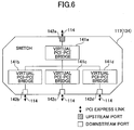
- Fig. 6 is a block diagram showing an example of a logical structure of the switch. As shown in Fig. 6, the switch is recognized as a group of virtual PCIPCI bridges 141 (141a to 141d) from configuration software. In Fig. 6, arrows show the PCI Express links 114, 126 (114b to 114f, 126c to 126f) and the reference numbers 142a to 142d show ports.
- the port 142a is an upstream port near the root complex and the ports 142b to 142d are downstream ports far from the root complex.
- the PCI Express link 114e to the PCI bridge 119 gives a connection from PCI Express to PCI/PCI-X.
- the existing PCI/PCI-X devices can be used on the PCI Express system.
- Fig. 7A is a block diagram showing existing PCI architecture.
- Fig. 7B is a block diagram showing PCI Express architecture.
- the existing PCI architecture has a structure in which the protocol closely relates to the signaling and does not have the concept of layers.
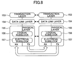
- the PCI Express architecture has a layered structure and the specification of each layer is defined, similar to the general communication protocol and InfiniBand (registered trademark). That is, the PCI Express architecture has a structure in which a transaction layer 153, a data link layer 154, and a physical layer 155 are disposed between a software layer 151 located in the uppermost position and a mechanical section 152 located in the lowest position.
- each module can be reused.
- the data link layer 154 and the transaction layer 153 can be used as they are and only the physical layer 155 is changed.
- Fig. 8 is a block diagram showing the layered structure of the PCI Express architecture.
- the transaction layer 153 is located in the uppermost position and has a function that assembles and separates TLPs (transaction layer packets).
- the TLP is used for transference of transactions, such as read/write, and various events.
- the transaction layer 153 executes flow control using a credit for the TLP.
- Fig. 9 is a diagram showing a format example of the TLP. In Fig. 9, an outline of the TLP is shown in relation to the layers 153 to 155. The details of the TLP are explained below.
- the main role of the data link layer 154 is to ensure data completeness of the TLP by error detection/correction (retransmission) and execute link management. Exchanging packets for the link management and the flow control are executed between the data link layers 154. These packets are called DLLPs (data link layer packets) so as to distinguish them from the TLPs.
- DLLPs data link layer packets
- the physical layer 155 includes circuits necessary for interface operations, such as a driver, an input buffer, a parallel to serial/serial to parallel converter, a PLL circuit, and an impedance matching circuit.
- the physical layer 155 has a function to initialize/maintain the interface as a logic function.
- the physical layer 155 has a role which makes the data link layer 154/the transaction layer 153 independent from signal technology being used in the actual link.
- an embedded clock is used for a hardware structure of PCI Express, where timing of the clock is embedded in data signals without using clock signals, and a clock is extracted based on a cross point of data signals at the reception side.
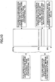
- Fig. 10 is a diagram showing a configuration memory space of PCI Express.
- PCI Express has a configuration space like the conventional PCI, the configuration space of the conventional PCI is 256 bytes; however, as shown in Fig. 10, the configuration space of the PCI Express is extended to 4096 bytes. With this configuration space, enough space is secured for a device such as a host bridge which will need many device intrinsic register sets in the future.
- access to the configuration space is executed by access (configuration read/write) to a flat memory space, and bus/device/function/register numbers are mapped in a memory register.
- a method using an I/O port can access the first 256 bytes in the configuration space, as a PCI configuration space.
- a function which converts conventional access into PCI Express access is installed in the host bridge.
- the range from 00h to 3Fh is a configuration header compatible with PCI 2.3.
- a conventional OS and software can be used as they are except for functions extended by PCI Express. That is, the software layer 151 in PCI Express succeeds to load/store architecture (a processor directly accesses an I/O register) which maintains the compatibility with the existing PCI.
- functions extended by PCI Express such as synchronized transfer, RAS (reliability, availability, and serviceability) functions, are used, it is required to access the PCI Express extended space of 4K bytes.
- PCI Express various form factors are assumed; however, as specific examples, there are an add-in card, a plug-in card (Express card), a mini PCI Express card, and so on.
- the transaction layer 153, the data link layer 154, and the physical layer 155 being the center of the PCI Express architecture are explained in detail.
- the main role of the transaction layer 153 is to assemble and separate TLPs between the upper software layer 151 and the lower data link layer 154.
- a message space is added, that is, four address spaces are defined.
- the message space is used for transmission (exchange) of messages, such as event notification in band and a general message between devices of PCI Express, and an interrupt request and acknowledgement is transferred by using the message as a virtual wire.
- a transaction type is defined in each of the address spaces.
- the memory space, the I/O space, and the configuration space are read/write types, and the message space is a basic type (including a vendor definition).
- PCI Express executes communications in a packet unit.
- the length of the header is 3DW (DW signifies double words and 3DW is 12 bytes) or 4DW (16 bytes).
- information such as the format of the TLP (the length of the header and the existence of a payload), the transaction type, a traffic class (TL), an attribute, and a payload length, is included.
- the maximum payload length in a packet is 1024 DW (4096 bytes).
- ECRC is used to ensure the completeness of data in end to end, and is 32 bits CRC in a part of the TLP.
- LCRC link CRC
- Upper software can give priority to traffic by using the TC.
- transferring image data can be given priority in transferring the image data and network data.
- the TC has eight classes TCO to TC7.
- Each of VCs is an independent virtual communication bus and has a resource (buffer and queue).
- the independent virtual communication buses are mechanisms which use plural independent data flow buffers using the same link in common.
- Fig. 11 is a schematic diagram explaining the concept of the VCs. As shown in Fig. 11, the VCs execute independent flow control. Even when a buffer of a VC is full, data can be transferred by another VC. That is, one link can be effectively used by dividing the physical one link into plural VCs. For example, as shown in Fig. 11, in a case where a link from a root complex (device) is divided into plural devices (components) via a switch, priority of traffic to each device (component) can be controlled.
- VCO is indispensable and other VCs (VC1 to VC7) are installed corresponding to a tradeoff of cost and performance.
- a continuous arrow line shows a default VC (VCO) and a broken arrow line shows other VCs (VC1 to VC7).
- the TC is mapped on the VC.
- the number of VCs is small, one or more TCs can be mapped on one VC.
- each TC is mapped on each VC one to one and all TCs are mapped on the VCO.
- the mapping of TCO on VCO is indispensable (fixed), and the other mapping is controlled by the upper software. The software can control the priority by utilizing the TCs.
- FC flow control
- the flow control is executed to establish transfer order by avoiding an overflow in a reception buffer.
- the flow control is executed point to point between links, not end to end. Consequently, a packet reaching a final destination (completer) cannot be acknowledged by the flow control.
- the flow control in PCI Express is executed by a credit base. That is, the following mechanism is used.
- the empty state of a reception side buffer is confirmed before starting the data transmission and overflow and underflow in the buffer are avoided.
- the reception side notifies a transmission side of buffer capacity (credit value) at the time of initializing the link, and the transmission side compares the credit value with the length of packets to be transmitted. When the credit value has remaining capacity, the packets are transmitted.
- Exchanging the information of the flow control is executed by using DLLP (data link layer packet) of the data link layer 154.
- the flow control is applied only to the TLP and is not applied to the DLLP. Therefore, the DLLP can always be transmitted/received.
- the main role of the data link layer 154 is to provide an exchanging function of the TLPs between two components on a link with high reliability.
- the data link layer 154 adds a sequence number of 2 bytes to its head and an LCRC (link CRC) of 4 Bytes to its tail of the TLP received from the transaction layer 153, and gives it to the physical layer 155 (refer to Fig. 9).
- the TLPs are stored in a retry buffer and retransmitted to a destination until an acknowledgment is received from the destination.
- the data link layer 154 decides that the link is abnormal and requires the physical layer 155 to execute retraining of the link.
- the state of the data link layer 154 is shifted to be inactive.
- the sequence number and the LCRC of the TLP received from the physical layer 155 of the transmission side are inspected, and when they are normal, the TLP is sent to the transaction layer 153; when they are abnormal, the reception side requires the transmission side to retransmit the TLP.
- a packet generated by the data link layer 154 is called a DLLP, and the DLLP is exchanged between the data link layers 154.
- the DLLP has the following types:
- the main role of the logical subblock 156 in the physical layer 155 is to convert a packet received from the data link layer 154 into a. packet which an electric subblock 157 can transmit (refer to Fig. 8). Further, the logical subblock 156 has a function of controlling/managing the physical layer 155.
- Fig. 13 is a schematic diagram showing a byte striping example in a ⁇ 4 link. As shown in Fig. 13, serial conversion is applied to the converted data and data from an LSB are transmitted in order on the lane. When plural lanes exist (a case of the x4 link is shown in Fig. 13), data are allocated to each lane in a byte unit before encoding. In this case, at first sight, this looks like a parallel bus; however, transferring is independently executed in each lane, consequently, skewing being a problem in the parallel bus can be greatly reduced.
- Fig. 14 is a diagram explaining the definition of link states L0, L0s, L1, and L2. As shown in Fig. 14, in order to make power consumption of links low, the link states L0, L0s, L1, and L2 are defined.
- the link state L0 is a normal mode and the power consumption is gradually lowered when the link state is changed from the L0s to L2; however, time requiring to return to the link state L0 becomes longer.
- the power consumption can be lowered to be as small as possible.
- the main role of the electrical subblock 157 in the physical layer 155 is to transmit data serialized by the logical subblock 156 to a lane, to receive data from a lane, and to send the received data to the logical subblock 156 (refer to Fig. 8).
- a capacitor for AC coupling is mounted in the transmission side of the link. With this, it is not necessary that a DC common mode voltage be the same in the transmission side and the reception side. Therefore, in the transmission side and the reception side, mutually different designing, a different specification of a semiconductor device, and a different power voltage can be used.
- the waveform of the reception side becomes small by the attenuation; however, in unchanging bits, the high frequency components are few and the waveform of the reception side becomes relatively large. Therefore, the de-emphasis is applied to make the waveform at the reception side constant.
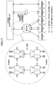
- Fig. 16 is a block diagram showing a configuration of the digital copying machine according to the embodiments of the present invention .
- a digital copying machine 1 includes a scanner 2 that reads image data of a manuscript, a plotter 3 that forms an image on a medium such as a paper based on the image data read by the scanner 1, a controller 4 that totally controls the digital copying machine 1, and an image data memory 5 that stores the image data.
- an electro-photographic system As printing systems of the image data by the plotter 3, there are various systems, such as, an electro-photographic system, an ink-jet system, a sublimation thermal transcription system, a sliver film photographic system, a direct thermo sensitive recording system, and a melting thermal transcription system, and any one of them can be used.
- an electro-photographic system As printing systems of the image data by the plotter 3, there are various systems, such as, an electro-photographic system, an ink-jet system, a sublimation thermal transcription system, a sliver film photographic system, a direct thermo sensitive recording system, and a melting thermal transcription system, and any one of them can be used.
- the digital copying machine 1 executes internal communications by using a data transferring system of the PCI Express standard.
- Fig. 17 is a block diagram showing a circuit configuration of a data transferring device 11 which executes data transfer in the data transferring system according to a first embodiment of the present invention.
- Configuration elements, such as the scanner 2, the plotter 3, the controller 4, and the image data memory 5 in the digital copying machine 1 mutually communicate by providing the data transferring device 11.
- the data transferring device 11 is composed of FIFO (first-in first-out) circuits and so on, and includes a line data storing section 12, a PCIe logic section 13, and a line data transfer controlling circuit 14.
- the line data storing section 12 temporarily stores input image data.
- the PCIe logic section 13 generates packets from the temporarily stored image data by using logic of the PCI Express standard and outputs the packets.
- the line data transfer controlling circuit 14 receives a line synchronizing signal LSYNC which transfers image data in each line and adjusts output timing of the packets by controlling the line data storing section 12 and the PCIe logic section 13.
- a frame synchronizing signal which transfers the image data in each frame can be used instead of using the line synchronizing signal LSYNC.
- the embodiments of the present invention are explained by using the line synchronizing signal LSYNC.
- the data transferring device 11 transfers image data by synchronizing with the line synchronizing signal LSYNC in the PCI Express standard with the control of the line data transfer controlling circuit 14.
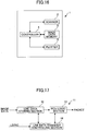
- Fig. 18A is a timing chart in conventional data transfer based on the PCI Express standard.
- Fig. 18B is a timing chart in the data transferring device 11 according to the first embodiment of the present invention.
- LSYNC is the line synchronizing signal as described above
- LGATE is a gate signal
- PCIe LINK STATE shows a link state in the link states of the PCI Express standard
- PCIe (Engine TX) shows outputs of image data (packets).
- the packets (image data) are transferred by causing a period between packets to be transferred in one line cycle of the line synchronizing signal LSYNC to be less than the time requiring to transit to the L0s state.
- This is a packet gathering unit.
- the number of the transition periods "t1" from the link state L0 to the link state L0s and from the link state L0s to link state L0 is reduced and the period of the L0s state in one line cycle is increased compared with the case shown in Fig. 18A. Therefore, the power saving can be realized compared with the conventional case.
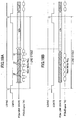
- Fig. 19A is the timing chart shown in Fig. 18B; however, explaining contents are different from those in Fig. 18B.
- Fig. 19B is a timing chart in the data transferring device 11 according to the modified example of the first embodiment of the present invention.
- the packets (image data) are transferred by causing a period between packets to be transferred in one line cycle of the line synchronizing signal LSYNC to be less than the time requiring to transit to the L0s state.
- a period between packets to be transferred in one line cycle of the line synchronizing signal LSYNC to be less than the time requiring to transit to the L0s state.
- Fig. 19A there is still a period “t2" between the packets (image data) to be transferred even though the period "t2" is less than the time requiring to transit to the L0s state.
- the period "t2" does not contribute to the image data transfer and is included in the state L0.
- the period "t2" is made “0" by the control of the line data transfer controlling circuit 14. With this control, the period of the link state L0 is shortened and the period of the state L0s is made longer. Therefore, further power saving can be realized compared with the case shown in Fig. 18B.
- the packets (image data) to be transferred are, for example, memory write request packets output from the controller 4 to the image data memory 5 and memory read completion packets output from the image data memory 5 to the controller 4.
- Fig. 20 is a block diagram showing a circuit configuration of a data transferring device 21 which executes data transfer in a data transferring system according to a second embodiment of the present invention.
- the data transferring device 21 includes plural data transferring devices 11 according to the first embodiment and a delay controlling circuit 22 that controls the line data transfer controlling circuits 14 in the data transferring devices 11.
- a delay controlling circuit 22 that controls the line data transfer controlling circuits 14 in the data transferring devices 11.
- three data transferring devices 11 are included in the data transferring device 21. Configuration elements in the data transferring device 11 are explained above; therefore, the same explanation is omitted.
- LSYNC line synchronizing signal
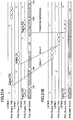
- Fig. 21A is a timing chart in conventional data transfer based on the PCI Express standard.
- Fig. 21B is a timing chart in the data transferring device 21 according to the second embodiment of the present invention.
- FIGs. 21A and 21B packets (image data) (PCIe(Engine TX0 to Tx2)), which are output from the data transferring devices 11 by synchronizing with the line synchronizing signals LSYNC0, LSYNC1, and LSYNC2, are shown as Engine TX0, Engine TX1, and Engine TX2.
- PCIe image data
- the image data Engine TX0, Engine TX1, and Engine TX2 are respectively output from the data transferring devices 11 by synchronizing with the line synchronizing signals LSYNC0, LSYNC1, and LSYNC2 without control. Therefore, as shown in Fig. 21A, between the periods of the link state L0 where the image data Engine TX0, Engine TX1, and Engine TX2 are output, many periods of the link state L0s occur, and before and after each link state L0s, many transition periods from the link state L0 to the link state L0s and from the link state L0s to the link state L0 are generated.
- the delay controlling circuit 22 delays the transferring time of one or two image data Engine TXns by making an image data Engine TXn' a transfer reference.
- the transferring time of the other image data Engine TX0 and Engine TX1 transmitted before transmitting the image data Engine TX2 is delayed.
- the period between the image data Engine TX0 and Engine TX1 and the period between the image data Engine TX1 and Engine TX2 are controlled to be shorter than the time which is required to transit to the link state L0s. This is also a packet gathering unit.
- the period of the link state L0s can be longer by reducing the transition period from the link state L0 to the link state Las and the transition period from the link state L0s to the link state L0 by gathering the link state L0 periods and the link state L0s periods, compared with the case of Fig. 21A.
- the present invention is based on Japanese Priority Patent Application No. 2005-011262, filed on January 19, 2005, with the Japanese Patent Office, the entire contents of which are hereby incorporated by reference.
Landscapes
- Engineering & Computer Science (AREA)
- Theoretical Computer Science (AREA)
- Physics & Mathematics (AREA)
- General Engineering & Computer Science (AREA)
- General Physics & Mathematics (AREA)
- Information Transfer Systems (AREA)
- Communication Control (AREA)
- Facsimiles In General (AREA)
- Power Sources (AREA)
Applications Claiming Priority (1)
| Application Number | Priority Date | Filing Date | Title |
|---|---|---|---|
| JP2005011262A JP4704050B2 (ja) | 2005-01-19 | 2005-01-19 | データ転送システム及び電子機器 |
Publications (3)
| Publication Number | Publication Date |
|---|---|
| EP1684188A2 true EP1684188A2 (fr) | 2006-07-26 |
| EP1684188A3 EP1684188A3 (fr) | 2007-07-11 |
| EP1684188B1 EP1684188B1 (fr) | 2009-03-04 |
Family
ID=36320204
Family Applications (1)
| Application Number | Title | Priority Date | Filing Date |
|---|---|---|---|
| EP06250258A Expired - Lifetime EP1684188B1 (fr) | 2005-01-19 | 2006-01-18 | Système et appareil électronique de transfert de données |
Country Status (4)
| Country | Link |
|---|---|
| US (1) | US7454540B2 (fr) |
| EP (1) | EP1684188B1 (fr) |
| JP (1) | JP4704050B2 (fr) |
| DE (1) | DE602006005403D1 (fr) |
Cited By (2)
| Publication number | Priority date | Publication date | Assignee | Title |
|---|---|---|---|---|
| EP1764704A3 (fr) * | 2005-08-30 | 2007-08-29 | Ricoh Company, Ltd. | Système de traitement d'informations, procédé de transfert de données et produit informatique |
| US8090967B2 (en) | 2008-05-23 | 2012-01-03 | Intel Corporation | Power state transition initiation control of memory interconnect based on early warning signal, memory response time, and wakeup delay |
Families Citing this family (14)
| Publication number | Priority date | Publication date | Assignee | Title |
|---|---|---|---|---|
| US7664904B2 (en) | 2006-03-10 | 2010-02-16 | Ricoh Company, Limited | High speed serial switch fabric performing mapping of traffic classes onto virtual channels |
| JP4878185B2 (ja) * | 2006-03-17 | 2012-02-15 | 株式会社リコー | データ通信回路および調停方法 |
| JP5108261B2 (ja) * | 2006-07-11 | 2012-12-26 | 株式会社リコー | 情報処理装置およびデータ通信装置 |
| US8139574B2 (en) * | 2006-08-18 | 2012-03-20 | George Madathilparambil George | Creation and transmission of part of protocol information corresponding to network packets or datalink frames separately |
| JP4275168B2 (ja) * | 2006-11-30 | 2009-06-10 | シャープ株式会社 | Nicを備えるシステム機器および同システム機器の省電力制御方法 |
| JP4275169B2 (ja) * | 2006-11-30 | 2009-06-10 | シャープ株式会社 | Nicを備えたシステム機器および同システム機器の省電力制御方法 |
| US8582448B2 (en) * | 2007-10-22 | 2013-11-12 | Dell Products L.P. | Method and apparatus for power throttling of highspeed multi-lane serial links |
| JP5182513B2 (ja) * | 2007-12-27 | 2013-04-17 | 株式会社リコー | 画像処理装置及びその省電力制御方法 |
| KR100973079B1 (ko) * | 2008-08-13 | 2010-07-29 | 한국전자통신연구원 | 고속 PCIe 신호 전송 장치 및 그 제어방법 |
| US9025194B2 (en) | 2010-12-01 | 2015-05-05 | Canon Kabushiki Kaisha | Data transmission apparatus for transferring data to an output device for outputting data, printer, information processing apparatus, and control method thereof |
| JP2012118821A (ja) * | 2010-12-01 | 2012-06-21 | Canon Inc | データ転送装置、プリンタ、制御方法 |
| EP2474938B1 (fr) | 2011-01-05 | 2018-12-26 | Ricoh Company, Ltd. | Appareil et système de formation d'images |
| JP5754273B2 (ja) | 2011-07-11 | 2015-07-29 | 株式会社リコー | メモリ制御装置、情報処理装置およびメモリ制御方法 |
| JP6289147B2 (ja) * | 2014-02-14 | 2018-03-07 | 三菱電機株式会社 | データ伝送装置、データ伝送システム、キャリブレーション方法及びプログラム |
Citations (1)
| Publication number | Priority date | Publication date | Assignee | Title |
|---|---|---|---|---|
| US20040103333A1 (en) | 2002-11-22 | 2004-05-27 | Martwick Andrew W. | Apparatus and method for low latency power management on a serial data link |
Family Cites Families (14)
| Publication number | Priority date | Publication date | Assignee | Title |
|---|---|---|---|---|
| JPS61296838A (ja) * | 1985-06-25 | 1986-12-27 | Nec Corp | パケツト交換網における伝送デ−タ中継制御方式 |
| JPH01175431A (ja) * | 1987-12-29 | 1989-07-11 | Nec Corp | パケット通信方式 |
| JPH01241243A (ja) * | 1988-03-23 | 1989-09-26 | Mitsubishi Electric Corp | パケット交換装置 |
| JP2001308919A (ja) * | 2000-04-25 | 2001-11-02 | Oki Electric Ind Co Ltd | 通信装置 |
| JP2002026927A (ja) * | 2000-07-10 | 2002-01-25 | Pfu Ltd | カプセリング方法及び装置並びにプログラム記録媒体 |
| JP3991594B2 (ja) | 2001-02-02 | 2007-10-17 | 富士ゼロックス株式会社 | データ処理装置 |
| JP2003078565A (ja) * | 2001-08-30 | 2003-03-14 | Matsushita Electric Ind Co Ltd | 無線通信装置 |
| US6801970B2 (en) * | 2001-09-30 | 2004-10-05 | Hewlett-Packard Development Company, L.P. | Priority transaction support on the PCI-X bus |
| JP2003229857A (ja) * | 2002-01-31 | 2003-08-15 | Alpine Electronics Inc | シリアルバスシステム、シリアルバスの帯域管理機器および通信機器 |
| JP2003324445A (ja) * | 2002-05-07 | 2003-11-14 | Alps Electric Co Ltd | 無線伝送方式 |
| US7178045B2 (en) | 2003-12-30 | 2007-02-13 | Intel Corporation | Optimizing exit latency from an active power management state |
| US20050248584A1 (en) | 2004-05-10 | 2005-11-10 | Koji Takeo | Imaging system and image processing apparatus |
| US20050254085A1 (en) | 2004-05-12 | 2005-11-17 | Koji Oshikiri | Image forming system |
| US7500029B2 (en) * | 2004-10-29 | 2009-03-03 | Intel Corporation | Maximal length packets |
-
2005
- 2005-01-19 JP JP2005011262A patent/JP4704050B2/ja not_active Expired - Fee Related
-
2006
- 2006-01-17 US US11/332,203 patent/US7454540B2/en not_active Expired - Fee Related
- 2006-01-18 EP EP06250258A patent/EP1684188B1/fr not_active Expired - Lifetime
- 2006-01-18 DE DE602006005403T patent/DE602006005403D1/de not_active Expired - Lifetime
Patent Citations (1)
| Publication number | Priority date | Publication date | Assignee | Title |
|---|---|---|---|---|
| US20040103333A1 (en) | 2002-11-22 | 2004-05-27 | Martwick Andrew W. | Apparatus and method for low latency power management on a serial data link |
Cited By (3)
| Publication number | Priority date | Publication date | Assignee | Title |
|---|---|---|---|---|
| EP1764704A3 (fr) * | 2005-08-30 | 2007-08-29 | Ricoh Company, Ltd. | Système de traitement d'informations, procédé de transfert de données et produit informatique |
| US7536489B2 (en) | 2005-08-30 | 2009-05-19 | Ricoh Company Limited | Information processing system for determining payload size based on packet-to-payload size ratio |
| US8090967B2 (en) | 2008-05-23 | 2012-01-03 | Intel Corporation | Power state transition initiation control of memory interconnect based on early warning signal, memory response time, and wakeup delay |
Also Published As
| Publication number | Publication date |
|---|---|
| DE602006005403D1 (de) | 2009-04-16 |
| US7454540B2 (en) | 2008-11-18 |
| EP1684188A3 (fr) | 2007-07-11 |
| EP1684188B1 (fr) | 2009-03-04 |
| JP2006201909A (ja) | 2006-08-03 |
| JP4704050B2 (ja) | 2011-06-15 |
| US20060171300A1 (en) | 2006-08-03 |
Similar Documents
| Publication | Publication Date | Title |
|---|---|---|
| EP1879115B1 (fr) | Appareil de traitement d'informations et dispositif de communication de données | |
| EP1832984B1 (fr) | Appareil de traitement d'informations, système de traitement d'informations et procédé de communication de données | |
| EP1681817B1 (fr) | Dispositif de communication, dispositif électronique, dispositif de prise d'images | |
| EP1684188B1 (fr) | Système et appareil électronique de transfert de données | |
| US20060209722A1 (en) | Data transferring system and electronic apparatus | |
| US7755791B2 (en) | Image processing apparatus and image forming apparatus | |
| JP5151176B2 (ja) | データ通信装置、画像処理システムおよびデータ通信方法 | |
| US20050254085A1 (en) | Image forming system | |
| JP4308680B2 (ja) | 画像形成装置 | |
| US20060187944A1 (en) | Communication device, data transferring system and electronic apparatus | |
| JP4287325B2 (ja) | 画像システム | |
| JP4928715B2 (ja) | シリアルデータ転送装置、画像出力装置、画像入力装置及び画像形成装置 | |
| JP4564740B2 (ja) | 画像機器システム | |
| JP4777723B2 (ja) | 情報処理システム、プログラムおよびデータ転送方法 | |
| JP5218377B2 (ja) | 画像形成システム | |
| JP2005346629A (ja) | 画像処理装置 | |
| JP2006113798A (ja) | データ転送システム、受信バッファ装置、データ転送システムの仕様設定方法及び画像形成システム | |
| JP2007282187A (ja) | 情報処理装置、情報処理システムおよびデータ通信方法 | |
| JP2007272871A (ja) | 情報処理装置およびデータ通信方法 | |
| JP4690828B2 (ja) | 情報処理システム、プログラムおよびパケット通信方法 | |
| JP4824422B2 (ja) | 制御装置、画像処理システムおよびデータ転送経路切替方法 | |
| JP2007226494A (ja) | データ転送システム | |
| JP2005332372A (ja) | 画像処理装置及び画像形成装置 |
Legal Events
| Date | Code | Title | Description |
|---|---|---|---|
| PUAI | Public reference made under article 153(3) epc to a published international application that has entered the european phase |
Free format text: ORIGINAL CODE: 0009012 |
|
| 17P | Request for examination filed |
Effective date: 20060203 |
|
| AK | Designated contracting states |
Kind code of ref document: A2 Designated state(s): AT BE BG CH CY CZ DE DK EE ES FI FR GB GR HU IE IS IT LI LT LU LV MC NL PL PT RO SE SI SK TR |
|
| AX | Request for extension of the european patent |
Extension state: AL BA HR MK YU |
|
| PUAL | Search report despatched |
Free format text: ORIGINAL CODE: 0009013 |
|
| AK | Designated contracting states |
Kind code of ref document: A3 Designated state(s): AT BE BG CH CY CZ DE DK EE ES FI FR GB GR HU IE IS IT LI LT LU LV MC NL PL PT RO SE SI SK TR |
|
| AX | Request for extension of the european patent |
Extension state: AL BA HR MK YU |
|
| AKX | Designation fees paid |
Designated state(s): DE FR GB IT |
|
| 17Q | First examination report despatched |
Effective date: 20080307 |
|
| GRAP | Despatch of communication of intention to grant a patent |
Free format text: ORIGINAL CODE: EPIDOSNIGR1 |
|
| GRAS | Grant fee paid |
Free format text: ORIGINAL CODE: EPIDOSNIGR3 |
|
| GRAA | (expected) grant |
Free format text: ORIGINAL CODE: 0009210 |
|
| AK | Designated contracting states |
Kind code of ref document: B1 Designated state(s): DE FR GB IT |
|
| REG | Reference to a national code |
Ref country code: GB Ref legal event code: FG4D |
|
| REF | Corresponds to: |
Ref document number: 602006005403 Country of ref document: DE Date of ref document: 20090416 Kind code of ref document: P |
|
| PLBE | No opposition filed within time limit |
Free format text: ORIGINAL CODE: 0009261 |
|
| STAA | Information on the status of an ep patent application or granted ep patent |
Free format text: STATUS: NO OPPOSITION FILED WITHIN TIME LIMIT |
|
| 26N | No opposition filed |
Effective date: 20091207 |
|
| PG25 | Lapsed in a contracting state [announced via postgrant information from national office to epo] |
Ref country code: IT Free format text: LAPSE BECAUSE OF FAILURE TO SUBMIT A TRANSLATION OF THE DESCRIPTION OR TO PAY THE FEE WITHIN THE PRESCRIBED TIME-LIMIT Effective date: 20090304 |
|
| PGFP | Annual fee paid to national office [announced via postgrant information from national office to epo] |
Ref country code: DE Payment date: 20140122 Year of fee payment: 9 |
|
| PGFP | Annual fee paid to national office [announced via postgrant information from national office to epo] |
Ref country code: FR Payment date: 20140123 Year of fee payment: 9 |
|
| PGFP | Annual fee paid to national office [announced via postgrant information from national office to epo] |
Ref country code: GB Payment date: 20140121 Year of fee payment: 9 |
|
| REG | Reference to a national code |
Ref country code: DE Ref legal event code: R119 Ref document number: 602006005403 Country of ref document: DE |
|
| GBPC | Gb: european patent ceased through non-payment of renewal fee |
Effective date: 20150118 |
|
| PG25 | Lapsed in a contracting state [announced via postgrant information from national office to epo] |
Ref country code: GB Free format text: LAPSE BECAUSE OF NON-PAYMENT OF DUE FEES Effective date: 20150118 Ref country code: DE Free format text: LAPSE BECAUSE OF NON-PAYMENT OF DUE FEES Effective date: 20150801 |
|
| REG | Reference to a national code |
Ref country code: FR Ref legal event code: ST Effective date: 20150930 |
|
| PG25 | Lapsed in a contracting state [announced via postgrant information from national office to epo] |
Ref country code: FR Free format text: LAPSE BECAUSE OF NON-PAYMENT OF DUE FEES Effective date: 20150202 |