EP1696006B1 - Encre métallique et substrate d'affichage et procédé de fabrication correspondant - Google Patents
Encre métallique et substrate d'affichage et procédé de fabrication correspondant Download PDFInfo
- Publication number
- EP1696006B1 EP1696006B1 EP05101515A EP05101515A EP1696006B1 EP 1696006 B1 EP1696006 B1 EP 1696006B1 EP 05101515 A EP05101515 A EP 05101515A EP 05101515 A EP05101515 A EP 05101515A EP 1696006 B1 EP1696006 B1 EP 1696006B1
- Authority
- EP
- European Patent Office
- Prior art keywords
- group
- metal
- nano particles
- promoting
- ink
- Prior art date
- Legal status (The legal status is an assumption and is not a legal conclusion. Google has not performed a legal analysis and makes no representation as to the accuracy of the status listed.)
- Expired - Lifetime
Links
Images
Classifications
-
- C—CHEMISTRY; METALLURGY
- C09—DYES; PAINTS; POLISHES; NATURAL RESINS; ADHESIVES; COMPOSITIONS NOT OTHERWISE PROVIDED FOR; APPLICATIONS OF MATERIALS NOT OTHERWISE PROVIDED FOR
- C09D—COATING COMPOSITIONS, e.g. PAINTS, VARNISHES OR LACQUERS; FILLING PASTES; CHEMICAL PAINT OR INK REMOVERS; INKS; CORRECTING FLUIDS; WOODSTAINS; PASTES OR SOLIDS FOR COLOURING OR PRINTING; USE OF MATERIALS THEREFOR
- C09D11/00—Inks
- C09D11/30—Inkjet printing inks
- C09D11/36—Inkjet printing inks based on non-aqueous solvents
-
- C—CHEMISTRY; METALLURGY
- C09—DYES; PAINTS; POLISHES; NATURAL RESINS; ADHESIVES; COMPOSITIONS NOT OTHERWISE PROVIDED FOR; APPLICATIONS OF MATERIALS NOT OTHERWISE PROVIDED FOR
- C09D—COATING COMPOSITIONS, e.g. PAINTS, VARNISHES OR LACQUERS; FILLING PASTES; CHEMICAL PAINT OR INK REMOVERS; INKS; CORRECTING FLUIDS; WOODSTAINS; PASTES OR SOLIDS FOR COLOURING OR PRINTING; USE OF MATERIALS THEREFOR
- C09D11/00—Inks
- C09D11/52—Electrically conductive inks
-
- C—CHEMISTRY; METALLURGY
- C09—DYES; PAINTS; POLISHES; NATURAL RESINS; ADHESIVES; COMPOSITIONS NOT OTHERWISE PROVIDED FOR; APPLICATIONS OF MATERIALS NOT OTHERWISE PROVIDED FOR
- C09D—COATING COMPOSITIONS, e.g. PAINTS, VARNISHES OR LACQUERS; FILLING PASTES; CHEMICAL PAINT OR INK REMOVERS; INKS; CORRECTING FLUIDS; WOODSTAINS; PASTES OR SOLIDS FOR COLOURING OR PRINTING; USE OF MATERIALS THEREFOR
- C09D11/00—Inks
- C09D11/30—Inkjet printing inks
- C09D11/38—Inkjet printing inks characterised by non-macromolecular additives other than solvents, pigments or dyes
-
- H—ELECTRICITY
- H01—ELECTRIC ELEMENTS
- H01B—CABLES; CONDUCTORS; INSULATORS; SELECTION OF MATERIALS FOR THEIR CONDUCTIVE, INSULATING OR DIELECTRIC PROPERTIES
- H01B1/00—Conductors or conductive bodies characterised by the conductive materials; Selection of materials as conductors
- H01B1/20—Conductive material dispersed in non-conductive organic material
- H01B1/24—Conductive material dispersed in non-conductive organic material the conductive material comprising carbon-silicon compounds, carbon or silicon
-
- H—ELECTRICITY
- H05—ELECTRIC TECHNIQUES NOT OTHERWISE PROVIDED FOR
- H05K—PRINTED CIRCUITS; CASINGS OR CONSTRUCTIONAL DETAILS OF ELECTRIC APPARATUS; MANUFACTURE OF ASSEMBLAGES OF ELECTRICAL COMPONENTS
- H05K1/00—Printed circuits
- H05K1/02—Details
- H05K1/09—Use of materials for the conductive, e.g. metallic pattern
- H05K1/092—Dispersed materials, e.g. conductive pastes or inks
- H05K1/097—Inks comprising nanoparticles and specially adapted for being sintered at low temperature
-
- H—ELECTRICITY
- H05—ELECTRIC TECHNIQUES NOT OTHERWISE PROVIDED FOR
- H05K—PRINTED CIRCUITS; CASINGS OR CONSTRUCTIONAL DETAILS OF ELECTRIC APPARATUS; MANUFACTURE OF ASSEMBLAGES OF ELECTRICAL COMPONENTS
- H05K2203/00—Indexing scheme relating to apparatus or processes for manufacturing printed circuits covered by H05K3/00
- H05K2203/09—Treatments involving charged particles
- H05K2203/095—Plasma, e.g. for treating a substrate to improve adhesion with a conductor or for cleaning holes
-
- H—ELECTRICITY
- H05—ELECTRIC TECHNIQUES NOT OTHERWISE PROVIDED FOR
- H05K—PRINTED CIRCUITS; CASINGS OR CONSTRUCTIONAL DETAILS OF ELECTRIC APPARATUS; MANUFACTURE OF ASSEMBLAGES OF ELECTRICAL COMPONENTS
- H05K3/00—Apparatus or processes for manufacturing printed circuits
- H05K3/10—Apparatus or processes for manufacturing printed circuits in which conductive material is applied to the insulating support in such a manner as to form the desired conductive pattern
- H05K3/12—Apparatus or processes for manufacturing printed circuits in which conductive material is applied to the insulating support in such a manner as to form the desired conductive pattern using thick film techniques, e.g. printing techniques to apply the conductive material or similar techniques for applying conductive paste or ink patterns
- H05K3/1241—Apparatus or processes for manufacturing printed circuits in which conductive material is applied to the insulating support in such a manner as to form the desired conductive pattern using thick film techniques, e.g. printing techniques to apply the conductive material or similar techniques for applying conductive paste or ink patterns by ink-jet printing or drawing by dispensing
- H05K3/125—Apparatus or processes for manufacturing printed circuits in which conductive material is applied to the insulating support in such a manner as to form the desired conductive pattern using thick film techniques, e.g. printing techniques to apply the conductive material or similar techniques for applying conductive paste or ink patterns by ink-jet printing or drawing by dispensing by ink-jet printing
-
- H—ELECTRICITY
- H05—ELECTRIC TECHNIQUES NOT OTHERWISE PROVIDED FOR
- H05K—PRINTED CIRCUITS; CASINGS OR CONSTRUCTIONAL DETAILS OF ELECTRIC APPARATUS; MANUFACTURE OF ASSEMBLAGES OF ELECTRICAL COMPONENTS
- H05K3/00—Apparatus or processes for manufacturing printed circuits
- H05K3/38—Improvement of the adhesion between the insulating substrate and the metal
- H05K3/381—Improvement of the adhesion between the insulating substrate and the metal by special treatment of the substrate
-
- H—ELECTRICITY
- H05—ELECTRIC TECHNIQUES NOT OTHERWISE PROVIDED FOR
- H05K—PRINTED CIRCUITS; CASINGS OR CONSTRUCTIONAL DETAILS OF ELECTRIC APPARATUS; MANUFACTURE OF ASSEMBLAGES OF ELECTRICAL COMPONENTS
- H05K3/00—Apparatus or processes for manufacturing printed circuits
- H05K3/38—Improvement of the adhesion between the insulating substrate and the metal
- H05K3/389—Improvement of the adhesion between the insulating substrate and the metal by the use of a coupling agent, e.g. silane
Definitions
- This invention relates to a metal ink for ink jet printing of conductive lines and a method for manufacturing the same and a substrate for a display having a plurality of ink jet printed conductive lines and a method for manufacturing the same. More specifically, this invention relates to a metal ink and a substrate for a PDP having a plurality of ink jet printed conductive lines for address and bus electrodes.
- Silver nano-particle ink is composed of individually dispersed metal nanoparticles, surfactants and organic particles ( EP1349135A1 , US20040043691A1 , ULVAC).
- US2004/0038616A1 (Fujitsu) describes a method of manufacturing a substrate for a flat panel display, the method comprising: forming a plurality of grooves in the bottom of a float glass substrate by a subtractive process to form barrier ribs comprising protrusions remaining between the respective grooves, and then forming electrodes on the bottoms of the grooves by an ink-jet process or a dispensing process.
- An alternative process to form narrow metal lines on glass or ITO surfaces using the nano-particle ink is to treat the substrate moderately and to have a contact angle of 60° for the nano-particle ink ( US20030083203A , Seiko Epson; M.
- US 6,118,426 describes a process for creating an electronically addressable display which includes multiple printing operations, similar to a multi-color process in conventional screen printing. In some of the process steps, electrically non-active inks are printed onto areas of the receiving substrate, and in other steps, electrically active inks are printed onto different areas of the substrate.
- US 2003/168639 describes a metallic nano particle cluster ink and a method for forming a conductive metal pattern using the cluster ink.
- the metallic nano particle cluster ink comprises colloidal metallic nano particles and a bifunctional compound.
- the conductive metal pattern is formed by forming a metallic nano particle pattern on a substrate using a mold made from PDMS (poly(dimethylsiloxane)-polymer) as a stamp, and heat-treating the substrate.
- PDMS poly(dimethylsiloxane)-polymer
- EP 1383597 describes a metal nano particle colloid solution, metal-polymer nanocomposites, and methods for preparing the same.
- the metal nano particle colloid solution and the metal-polymer nanocomposites can be prepared with a variety of polymeric stabilizers and have uniform particle diameter and shape.
- the metal nano particle colloid solution and the metal-polymer nanocomposites have wide applications, for example, as an antibacterial agent, a sterilizer, a conductive adhesive, conductive ink or an electromagnetic wave shield for an image display.
- JP 2004/207659 describes a water-shedding printing part formed by printing a water-shedding ink in a non-circuit pattern region in the surface of a substrate.
- a water-system colloidal solution wherein conductive nano metallic powder of an average grain diameter of 0.1 to 50 nm is dispersed, is applied to the surface of the substrate, and the colloidal solution is attached to only the non-printing part of the substrate which becomes a circuit pattern region. Then, the substrate is heated, the conductive nano metallic powder is fused mutually by evaporating liquid alone in the colloidal solution, and a conductive metallic layer consisting of nano metallic powder is formed in the non-printing part. A circuit is manufactured in this way.
- one object of the invention is to improve the adhesion of ink jet printed conductive lines, for example ink jet printed address and bus electrodes on a ground substrate.
- Another object of the invention is to improve the abrasion resistance and the flexibility of ink jet printed conductive lines in order to increase the life time of said ground substrates and to allow flexible ground substrates.
- a metal ink for ink jet printing of conductive lines which results in an improvement of abrasion resistance and of flexibility of ink jet printed conductive lines. Therefore a metal ink according to the invention comprises dispersed metal nano powder and a solvent wherein the metal ink comprises anti abrasive promoting nano particles and/or flexible promoting polymers.
- the metal ink comprises anti abrasive promoting nano particles and/or flexible promoting polymers.
- dispersed metal nano powder comprises silver, gold, platinum, palladium nickel and/or copper.
- the anti abrasive promoting nano particles result in an improvement of abrasion resistance whereby the flexible promoting polymers result in an improvement of the flexibility of the (metal) ink jet printed conductive lines.
- the anti abrasive promoting nano particles are colloidal and/or fumed silica nano particles and/or sol-gel nano particles and/or carbon nano particles and the flexible promoting polymers are silicone polymers and/or functionalised silicone polymers.
- the silicone polymer comprises at least one polysiloxane of the formula (I): R 1 n R 2 m SiO( 4 - n - m ) /2 (I) wherein each R 1 , which may be identical or different, represents H, OH, a monovalent hydrocarbon group or a monovalent siloxane group; each R 2 which may be identical or different, represents a group comprising at least one reactive functional group, wherein m and n fulfil the requirements of 0 ⁇ n ⁇ 4, 0 ⁇ m ⁇ 4 and 2 ⁇ (m+n) ⁇ 4.
- each of R 2 represents a group comprising at least one reactive functional group selected from a hydroxyl group, a carboxyl group, an isocyanate group, a blocked polyisocyanate group, a primary amine group, a secondary amine group, an amide group, a carbamate group, a urea group, a urethane group, a vinyl group, an unsaturated ester group, a maleimide group, a fumarate group, an anhydride group, a hydroxy alkylamide group, and an epoxy group.
- a reactive functional group selected from a hydroxyl group, a carboxyl group, an isocyanate group, a blocked polyisocyanate group, a primary amine group, a secondary amine group, an amide group, a carbamate group, a urea group, a urethane group, a vinyl group, an unsaturated ester group, a maleimide group, a fumarate group, an anhydride group, a
- the silicone polymer comprises at least one polysiloxane of the formula (II) or (III) R 3 Si-O-(SiR 2 O-) n -(SiRR a O) m -SiR 3 (II) R a R 2 Si-O-(SiR 2 O-) n -(SiRR a O) m -SiR 2 R a (III) wherein m has a value of at least 1; m' ranges from 0 to 75; n ranges from 0 to 75; n' ranges from 0 to 75; each R, which may be identical or different, is selected from H, OH, monovalent hydrocabon groups, monovalent siloxane groups, and mixtures of any of the foregoing; and R a comprises the following formula (IV): -R 3 -X (IV) wherein -R 3 is selected from an alkylene group, an oxyalkylene group, an alkylene aryl
- the metal nano powder of the ink and the above-mentioned anti abrasive promoting nano particles/flexible promoting polymers are crosslinked according to the invention.
- the cross linking is carried out during the sintering of the ink which is preferably carried after the ink jet printing of the ink, for example after the ink jet printing of the ink for forming conductive lines on a substrate.
- the method for producing a metal ink with improved abrasion resistance is characterised by mixing anti abrasive promoting nano particles and/or flexible promoting polymers into common metal ink.
- anti abrasive promoting nano particles and/or flexible promoting polymers Preferably colloidal and/or fumed silica nano particles and/or sol-gel nano particles and/or carbon nano particles are used as anti abrasive promoting nano particles and silicone polymers and/or functionalised silicone polymers are used as flexible promoting polymers.
- the mixing process is performed by sonication.
- a surface modification of silica particles is performed by condensation reactions with silanes having at least one metal adhesion functional group, wherein the metal adhesion functional group has at least one N, O, S and/or P-atom.
- the metal adhesion functional group is selected from amine, diamine, triamine, tetraamine, polyamine, pyridine, imidazole, carboxylic acid, sulfonic acid, phosphate, phosphonate or phenol.
- sol-gel nano particles are synthesised from co-condensation reactions of organo(alkoxy)-silanes with at least one organic functional group, wherein at least N, O, S and/or P-atom is present or transition metal alkoxides or their copolymerisation reactions with each other or with organic molecules are present.
- a substrate for a display having a plurality of ink jet printed conductive lines with improved adhesion of ink jet printed conductive lines and/or improved abrasion resistance and the flexibility of ink jet printed conductive lines comprises a metal adhesion promoting layer which is disposed between said ground substrate and conductive lines and the substrate furthermore comprises colloidal and/or fumed silica nano particles and/or sol-gel nano particles and/or carbon nano particles and/or silicone polymers and/or functionalised silicone polymers which are attached to said ground substrate and to said conductive lines.
- the organic group comprises at least amine, diamine, triamine, tetraamine, polyamine, amide, polyamide, hydrazine, pyridine, imidazole, thiophene, carboxylic acid, carboxylic acid halogenide, sulfide, disulfide, trisulfide, tetrasulfide, polysulfide, sulfonic acid, sulfonic acid halogenide, phosphate, phosphonate, epoxide, phenol and/or polyether.
- a method for the manufacture of a substrate for a display having a plurality of conductive lines with improved adhesion and/or improved abrasion resistance and the flexibility of ink jet printed conductive lines comprises the steps of:
- the metal adhesion promoting layer is applied by a plasma treatment of NH 3 , H 2 S and/or PH 3 or a plasma treatment of a substance of the formula (VI) or a plasma polymerisation of a silane with the formula (VII).
- a substance of the formula (IX) is used for the application of the metal adhesion promoting layer.
- the metal adhesion promoting layer is applied by a wet chemistry process.
- the metal adhesion promoting layer is applied by dipping the ground substrate into a solution of a substance of the formula (VI).
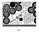
- Fig. 1 shows a substrate according to the invention in a sectional view.
- Crosslinked anti abrasive promoting nano particles 4, 6, 7 and flexible promoting polymers 5 are crosslinked to silver nano particles 3 (diameter preferably from 1-50 nm) and to ground substrate 1 via the adhesion promoting layer 2 (plasma polymerized hexamethylsilazane).
- Sol gel silica particles 6, silica particles 7 (for example AEROSIL R-900 from Degussa AG) and dispersed carbon particles 4 (for example PRINTEX L6 from CABOT Corp.) are bound to the silver particles 3 in order to improve the abrasion resistance of conductive lines formed by the metal nano ink. Furthermore the flexibility of the sintered metal nano ink is improved by flexible silicone polymers 5.
- Conductive lines formed by sintered ink (from the substances as described above) on the ground substrate 1 (ITO coated glass substrate) and the metal adhesion promoting layer 2 (plasma polymerized hexamethylsilazane) results in better abrasion resistance and better flexibility of said conductive lines.
- the silver particles 3 are bound to each other via the linkages 8.
- the flexible silicone polymer 5 is bound via the linkages 11 to the metal adhesion promoting layer 2.
- the flexible silicone polymer 5 is bound via the linkages 12 to the silver particles 3.
- the flexible silicone polymer 5 is bound via the linkages 13 to the sol gel particles 6.
- the silica particles 7 are bound via the linkages 14 to the silver particles 3.
- the silica particles 7 are bound via the linkages 15 to the metal adhesion promoting layer 2.
- the flexible silicone polymer 5 is bound via the linkages 16 to the silica particles 7.
- the silver particles 3 are bound via the linkages 17 to the sol gel particles 6.
- a typical manufacturing process of a metal ink composition including abrasion resistance, adhesion and flexibility promoting nanoscaled additive composites can be described as follows:
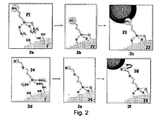
- amino-functionalised silica particles 22 are prepared as shown in Fig. 2a - 2b .
- 10 g of silica particles 7 (for example AEROSIL R-900 from Degussa AG) are dispersed in 300 ml of a 10 -1 -10 -3 mol/l ethanol solution of (3-aminopropyl)triethoxysilane 21 (functioning as a metal adhesion promoting silane).
- the mixture is stirred for 1-20 hours at 40-50°C and is dried at 40-100°C.
- the yielded amino-functionalised silica particles 22 are stored at room temperature.
- epoxy-functionalised silica particles 25 are prepared as shown in Fig. 2d - 2e .
- 10 g of silica particles 7 (for example AEROSIL R-900 from Degussa AG) are dispersed in 300 ml of a 10 -1 -10 -3 mol/l ethanol solution of (3-glycidoxypropyl)trimethoxysilane 24 (functioning as a metal adhesion promoting silane).
- the mixture is stirred for 1-20 hours at 40-50°C and is dried at 40-70 °C.
- the yielded epoxy-functionalised silica particles 25 are stored at room temperature.
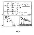
- epoxy-functionalised polysiloxane 20 is prepared as shown in Fig. 3a .
- 1,2-epoxy-5-hexene 19 and an amount of sodium bicarbonate equivalent to 20 to 25 ppm of total monomer solids is added under nitrogen atmosphere and the temperature is gradually increased up to 75°C.
- 5 % of a total amount of 7,1 g polysiloxane containing silicone hydride 18 (for example MASILWAX BASE from BASF Corp.) is added under agitation, followed by the addition of 0,02 g toluene, 0,005 g isopropanol and an equivalent to 10 ppm of chloroplatinic acid based on total monomer solids.
- reaction is then allowed to exotherm to 95°C at which time the remainder of the polysiloxane (containing silicone hydride) is added at a rate such that the temperature does not exceed 95°C. After completion of this addition, the reaction temperature is maintained at 95°C and monitored by infrared spectroscopy for disappearance of the silicone hydride absorption band (Si-H, 2150 cm -1 ).
- a fourth step the above prepared amino-functionalised silica particles 22 (see Fig. 2b ), epoxy-functionalised silica particles 24 (see Fig. 2e ) and the epoxy-functionalised polysiloxane 20 (see Fig. 3a ) as well as milled carbon nano particles 4 (e. g. PRINTEX L6 from CABOT Corp.) and silver ink (i.e. silver nano particles 3 dissolved in a solvent) are mixed by a sonication process.
- the weight percentages of these additives range from 0.1-20.
- the epoxy-functionalised polysiloxane 20 can be bonded to amino-functionalised silica particles 22 as shown in Fig. 3b .
- the silver particles 3 can be bonded to amino-functionalised silica particles 22 as shown in Fig. 2c .
- the silver particles 3 can be bonded to epoxy-functionalised silica particles 24 as shown in Fig. 2f .
- the obtained silver nano ink composition can be ink jet printed on a ground substrate 1 having a adhesion promoter layer 2 (plasma polymerized hexamethylsilazane) using a multinozzle ink jet printer.
- a adhesion promoter layer 2 plasma polymerized hexamethylsilazane
- the bonding of epoxy-functionalised polysiloxane 20 to the adhesion promoter layer 2 is shown in Fig. 3c .
- the printed ground substrate is heated at 100-250°C for 20-70 minutes.
- the obtained substrate can be used for further process steps of a PDP manufacturing process.
- Ink jet printing of the silver nano ink composition results in an improvement of abrasion resistance, adhesion and flexibility of the cured silver line, which is important for high process requirements in PDP manufacturing, specially in the case of ink jet printed address and bus electrodes on flexible substrates.
- the presence of cross-linked ink additives, based on Si-O-C, C-N-C, C-N, C-O, C-S and C-P linkages can be detected by ESCA (Electron Spectroscopy for Chemical Analysis) and ATR-FTIR (Attenuated Total Reflectance Fourier Transform Infrared Spectroscopy).
- the average particle size can be determined by visually examining an electron micrograph of a transmission electron microscopy (TEM), measuring the diameter of the particles in the image, and calculating the average particle size based on the magnification of the TEM image.
- TEM transmission electron microscopy
Landscapes
- Chemical & Material Sciences (AREA)
- Engineering & Computer Science (AREA)
- Materials Engineering (AREA)
- Wood Science & Technology (AREA)
- Organic Chemistry (AREA)
- Life Sciences & Earth Sciences (AREA)
- Dispersion Chemistry (AREA)
- Nanotechnology (AREA)
- Microelectronics & Electronic Packaging (AREA)
- Physics & Mathematics (AREA)
- Spectroscopy & Molecular Physics (AREA)
- Manufacturing Of Printed Wiring (AREA)
- Inks, Pencil-Leads, Or Crayons (AREA)
- Chemically Coating (AREA)
Claims (18)
- Encre métallique pour l'impression à jet d'encre de lignes conductrices comprenant une nanopoudre métallique dispersée (3) et un solvant, dans laquelle l'encre métallique comprend- des nanoparticules améliorant la résistance à l'abrasion et- des polymères améliorant la flexibilité (5, 20),dans laquelle
les nanoparticules améliorant la résistance à l'abrasion sont- des nanoparticules de silice colloïdale et/ou pyrogénée (7, 22, 25) et/ou- des nanoparticules de sol-gel (6) et/ou- des nanoparticules de carbone (4) etdans laquelle
les polymères améliorant la flexibilité sont- des polymères de silicone (5) et/ou- des polymères de silicone fonctionnalisés (20). - Encre métallique selon la revendication 1, dans laquelle
le polymère de silicone (5, 20) comprend au moins un polysiloxane de formule (I) :
R1 nR2 mSiO(4-n-m) /2 (I)
où chacun des R1, qui peuvent être identiques ou différents, représente H, OH, un groupe hydrocarboné monovalent ou un groupe siloxane monovalent ; chacun des R2, qui peuvent être identiques ou différents, représente un groupe comprenant au moins un groupe fonctionnel réactif, et où m et n satisfont les conditions 0<n<4, 0<m<4 et 2≤(m+n)<4. - Encre métallique selon la revendication 2, dans laquelle
chacun des R2, qui peuvent être identiques ou différents, représente un groupe comprenant au moins un groupe fonctionnel réactif choisi parmi un groupe hydroxyle, un groupe carboxyle, un groupe isocyanate, un groupe polyisocyanate bloqué, un groupe amine primaire, un groupe amine secondaire, un groupe amide, un groupe carbamate, un groupe urée, un groupe uréthanne, un groupe vinyle, un groupe ester insaturé, un groupe maléimide, un groupe fumarate, un groupe anhydride, un groupe hydroxyalkylamide et un groupe époxy. - Encre métallique selon la revendication 1, dans laquelle
le polymère de silicone (5, 20) comprend au moins un polysiloxane de formule (II) ou (III)
R3Si-O- (SiR2O-)n- (SiRRaO)m-SiR3 (II)
RaR2Si-O- (SiR2O-) n'- (SiRRaO)m'-SiR2Ra (III)
où
m a une valeur d'au moins 1 ;
m' est compris entre 0 et 75 ;
n est compris entre 0 et 75 ;
n' est compris entre 0 et 75 ;
chacun des R, qui peuvent être identiques ou différents, est choisi parmi H, OH, des groupes hydrocarbonés monovalents, des groupes siloxane monovalents, et des mélanges de n'importe lesquels des précédents ; et
Ra comprend la formule (IV) suivant
-R3-X (IV)
où- R3 est choisi parmi un groupe alkylène, un groupe oxyalkylène, un groupe alkylène-aryle, un groupe alcénylène, un groupe oxyalcénylène et un groupe alcénylène-aryle ; et
X représente un groupe qui comprend au moins un groupe fonctionnel réactif choisi parmi un groupe hydroxyle, un groupe carboxyle, un groupe isocyanate, un groupe polyisocyanate bloqué, un groupe amine primaire, un groupe amine secondaire, un groupe amide, un groupe carbamate, un groupe urée, un groupe uréthanne, un groupe vinyle, un groupe ester insaturé, un groupe maléimide, un groupe fumarate, un groupe anhydride, un groupe hydroxyalkylamide et un groupe époxy. - Encre métallique selon la revendication 1, dans laquelle
le polymère de silicone (5, 20) comprend au moins un polysiloxane qui est le produit de réaction d'au moins l'un des corps réactionnels suivants :(i) au moins un polysiloxane de formule (V) :
R3Si-O- (siR2O-)n'-SiR3 (V)
où chacun des groupes substituants R, qui peuvent être identiques ou différents, représente un groupe choisi parmi H, OH, un groupe hydrocarboné monovalent, un groupe siloxane et des mélanges de n'importe lesquels des précédents ; au moins un des groupes représentés par R est H et n' est compris entre 0 et 100, en sorte que le pourcentage de teneur en Si-H dudit au moins un polysiloxane soit compris entre 2 et 50 pour cent ; et(ii) au moins une molécule qui comprend au moins un groupe hydroxyle primaire et au moins une liaison insaturée capable de subir une réaction d'hydrolyse. - Encre métallique selon l'une des revendications précédentes, dans laquelle
la nanopoudre métallique (3) et les additifs sont réticulés. - Procédé de production d'une encre métallique ayant une résistance à l'abrasion améliorée, dans lequel- une nanopoudre métallique dispersée (3) et- un solvant- des nanoparticules améliorant la résistance à l'abrasion et- des polymères améliorant la flexibilitésont mélangés,
dans lequel les nanoparticules améliorant la résistance à l'abrasion sont- des nanoparticules de silice colloïdale et/ou pyrogénée (7, 22, 25) et/ou- des nanoparticules de sol-gel (6) et/ou- des nanoparticules de carbone (4) etdans lequel les polymères améliorant la flexibilité sont- des polymères de silicone (5) et/ou- des polymères de silicone fonctionnalisés (20). - Procédé selon la revendication 7, dans lequel l'opération de mélange est effectuée par sonication.
- Procédé selon la revendication 8, dans lequel une modification de surface des particules de silice (7) est effectuée par des réactions de condensation avec des silanes (21, 24) ayant au moins un groupe fonctionnel d'adhérence au métal, où le groupe fonctionnel d'adhérence au métal comporte au moins un atome de N, 0, S et/ou P.
- Procédé selon la revendication 9, dans lequel le groupe fonctionnel d'adhérence au métal est choisi parmi les suivants : amine, diamine, triamine, tétraamine, polyamine, pyridine, imidazole, acide carboxylique, acide sulfonique, phosphate, phosphonate et/ou phénol.
- Procédé selon la revendication 7, dans lequel les nanoparticules de sol-gel (6) sont synthétisées par des réactions de co-condensation d'organo(alkoxy)silanes avec au moins un groupe fonctionnel organique, où au moins un atome de N, O, S et/ou P est présent ou des alcoolates de métaux de transition ou leurs produits réactionnels de copolymérisation entre eux ou avec des molécules organiques sont présents.
- Substrat pour dispositif d'affichage, comprenant un substrat de base (1) ayant une pluralité de lignes conductrices comprenant une nanopoudre métallique, des nanoparticules améliorant la résistance à l'abrasion et des polymères améliorant la flexibilité sous forme réticulée, les nanoparticules améliorant la résistance à l'abrasion étant choisies parmi :- des nanoparticules de silice colloïdale et/ou pyrogénée (7, 22, 25) et/ou- des nanoparticules de sol-gel (6) et/ou- des nanoparticules de carbone (4)
et les polymères améliorant la flexibilité étant choisis parmi :- des polymères de silicone (5) et/ou- des polymères de silicone fonctionnalisés (20)où Y est un atome de N, S ou P et R est un atome de H et/ou au moins un groupe alkyle,
et une couche améliorant l'adhérence au métal (2) et lesdites lignes conductrices sont attachées à ladite couche améliorant l'adhérence au métal (2),
et
la couche améliorant l'adhérence au métal (2) comprend des molécules réticulées de formule (VI),
YRn n = 2, 3 (VI)
des molécules réticulées de formule (VII),
ZR'm ID m = 2, 3 (VII)
où Z est un atome de N, S ou P, et R' est un atome de H et/ou au moins un groupe silane ayant la formule (VIII)
SiR"3 (VIII)
où les R" sont des groupes alkyle qui peuvent être identiques ou différents, ou des molécules réticulées de formule (IX)
R Si X4 (IX)
où R est un atome de H, un groupe OH, un atome de Cl et/ou un groupe alkoxy, et les X sont chacun indépendamment un atome de H, un groupe OH, un atome de Cl, un groupe alkoxy, un groupe alkyle et/ou un groupe organique, le groupe organique comprenant au moins un groupe de liaison au métal. - Substrat selon la revendication 12, dans lequel
le groupe organique comprend au moins un des suivants : amine, diamine, triamine, tétraamine, polyamine, amide, polyamide, hydrazine, pyridine, imidazole, thiophène, acide carboxylique, halogénure d'acide carboxylique, sulfure, disulfure, trisulfure, tétrasulfure, polysulfure, acide sulfonique, halogénure d'acide sulfonique, phosphate, phosphonate, époxyde, phénol et/ou polyéther. - Procédé pour la fabrication d'un substrat pour dispositif d'affichage ayant une pluralité de lignes conductrices comprenant les étapes :- d'application d'une couche améliorant l'adhérence au métal (2) sur un substrat de base (1),- d'application d'une pluralité de lignes conductrices par impression à jet d'encre avec une encre métallique,dans lequel
une encre métallique comprenant une nanopoudre métallique, des nanoparticules améliorant la résistance à l'abrasion et des polymères améliorant la flexibilité sous forme réticulée, les nanoparticules améliorant la résistance à l'abrasion étant choisies parmi :- des nanoparticules de silice colloïdale et/ou pyrogénée (7, 22, 25) et/ou- des nanoparticules de sol-gel (6) et/ou- des nanoparticules de carbone (4)et les polymères améliorant la flexibilité étant choisis parmi- des polymères de silicone (5) et/ou- des polymères de silicone fonctionnalisés (20)
est utilisée pour le procédé d'impression à jet d'encre pour former les lignes conductrices,
et
la couche améliorant l'adhérence au métal (2) est appliquée par :
traitement au plasma avec NH3, H2S et/ou PH3
ou
traitement au plasma avec une substance de formule (VI)
ou
polymérisation au plasma d'un silane de formule (VII). - Procédé selon la revendication 14, dans lequel une substance de formule (IX) est utilisée pour l'application de la couche améliorant l'adhérence au métal (2).
- Procédé selon l'une des revendications 14 ou 15, dans
lequel
la couche améliorant l'adhérence au métal (2) est appliquée par un traitement chimique par voie humide. - Procédé selon la revendication 16, dans lequel la couche améliorant l'adhérence au métal (2) est appliquée en plongeant le substrat de base (1) dans une solution d'une substance de formule (VI).
- Utilisation d'une encre métallique selon l'une quelconque des revendications 1 à 6 pour la formation d'une pluralité de lignes conductrices sur un substrat pour dispositif d'affichage, dans laquelle une nanopoudre métallique, des nanoparticules améliorant la résistance à l'abrasion, qui sont des nanoparticules de silice colloïdale et/ou pyrogénée (7, 22, 25) et/ou des nanoparticules de sol-gel (6) et/ou des nanoparticules de carbone (4), et des polymères améliorant la flexibilité, qui sont des polymères de silicone (5) et/ou des polymères de silicone fonctionnalisés (20), sont réticulés pendant le frittage de l'encre après l'application de l'encre par impression à jet d'encre.
Priority Applications (7)
| Application Number | Priority Date | Filing Date | Title |
|---|---|---|---|
| DE602005014933T DE602005014933D1 (de) | 2005-02-28 | 2005-02-28 | Metallische Tinte und Substrat für eine Anzeige und deren Fertigungsmethode |
| AT05101515T ATE434024T1 (de) | 2005-02-28 | 2005-02-28 | Metallische tinte und substrat für eine anzeige und deren fertigungsmethode |
| EP05101515A EP1696006B1 (fr) | 2005-02-28 | 2005-02-28 | Encre métallique et substrate d'affichage et procédé de fabrication correspondant |
| KR1020050051991A KR100968429B1 (ko) | 2005-02-28 | 2005-06-16 | 금속 잉크, 금속 잉크 생산 방법, 표시장치용 기판 및표시장치용 기판의 제조 방법 |
| US11/361,362 US20060192183A1 (en) | 2005-02-28 | 2006-02-24 | Metal ink, method of preparing the metal ink, substrate for display, and method of manufacturing the substrate |
| JP2006050808A JP2006241455A (ja) | 2005-02-28 | 2006-02-27 | 金属インク、金属インクの製造方法、表示装置用の基板及び表示装置用の基板の製造方法 |
| CNA2006100592461A CN1869134A (zh) | 2005-02-28 | 2006-02-28 | 金属油墨、制备该金属油墨的方法、用于显示器的衬底及衬底的制造方法 |
Applications Claiming Priority (1)
| Application Number | Priority Date | Filing Date | Title |
|---|---|---|---|
| EP05101515A EP1696006B1 (fr) | 2005-02-28 | 2005-02-28 | Encre métallique et substrate d'affichage et procédé de fabrication correspondant |
Publications (2)
| Publication Number | Publication Date |
|---|---|
| EP1696006A1 EP1696006A1 (fr) | 2006-08-30 |
| EP1696006B1 true EP1696006B1 (fr) | 2009-06-17 |
Family
ID=34938839
Family Applications (1)
| Application Number | Title | Priority Date | Filing Date |
|---|---|---|---|
| EP05101515A Expired - Lifetime EP1696006B1 (fr) | 2005-02-28 | 2005-02-28 | Encre métallique et substrate d'affichage et procédé de fabrication correspondant |
Country Status (5)
| Country | Link |
|---|---|
| EP (1) | EP1696006B1 (fr) |
| KR (1) | KR100968429B1 (fr) |
| CN (1) | CN1869134A (fr) |
| AT (1) | ATE434024T1 (fr) |
| DE (1) | DE602005014933D1 (fr) |
Cited By (1)
| Publication number | Priority date | Publication date | Assignee | Title |
|---|---|---|---|---|
| EP3685915A1 (fr) * | 2008-09-01 | 2020-07-29 | Allgemeine Gold- und Silberscheideanstalt AG | Catalyseur d'argent pour la préparation de formaldéhyde |
Families Citing this family (16)
| Publication number | Priority date | Publication date | Assignee | Title |
|---|---|---|---|---|
| KR100768341B1 (ko) * | 2005-11-09 | 2007-10-17 | 주식회사 나노신소재 | 금속성 잉크, 그리고 이를 이용한 전극형성방법 및 기판 |
| US20080070146A1 (en) | 2006-09-15 | 2008-03-20 | Cabot Corporation | Hydrophobic-treated metal oxide |
| US8202502B2 (en) * | 2006-09-15 | 2012-06-19 | Cabot Corporation | Method of preparing hydrophobic silica |
| US8435474B2 (en) | 2006-09-15 | 2013-05-07 | Cabot Corporation | Surface-treated metal oxide particles |
| US8455165B2 (en) | 2006-09-15 | 2013-06-04 | Cabot Corporation | Cyclic-treated metal oxide |
| KR100850771B1 (ko) | 2007-02-21 | 2008-08-06 | 연세대학교 산학협력단 | 나노금속잉크 제조방법 |
| KR100935168B1 (ko) * | 2007-09-21 | 2010-01-06 | 삼성전기주식회사 | 비수계 전도성 나노잉크 조성물 |
| US20090191356A1 (en) * | 2008-01-28 | 2009-07-30 | Hee Hyun Lee | Method for forming a thin layer of particulate on a substrate |
| KR100979515B1 (ko) * | 2008-04-03 | 2010-09-02 | (주) 파루 | 롤투롤 인쇄방식을 이용한 rf 인쇄 정류기 |
| CN104672991B (zh) * | 2013-11-26 | 2017-07-04 | 比亚迪股份有限公司 | 一种铜导电墨水的制备方法 |
| CN110079783A (zh) | 2014-03-18 | 2019-08-02 | 3D-奥克赛茨公司 | 标签装置、其用途和用于标签装置的包装 |
| CN107113982B (zh) * | 2014-12-25 | 2020-04-10 | 住友电气工业株式会社 | 印刷配线板用基板、制作印刷配线板用基板的方法、印刷配线板、制作印刷配线板的方法以及树脂基材 |
| KR102407539B1 (ko) * | 2015-08-26 | 2022-06-13 | 엘지디스플레이 주식회사 | 하드코팅층, 이의 제조 방법 및 이를 포함하는 표시장치 |
| CN114763441A (zh) * | 2021-05-27 | 2022-07-19 | 上海博耳精细化学有限公司 | 一种消杂散光油墨及其应用 |
| CN118006164B (zh) * | 2024-02-04 | 2025-12-16 | 厦门大学 | 一种自封装耐高温电子墨水及制备方法和应用 |
| CN119694629A (zh) * | 2025-02-25 | 2025-03-25 | 西安稀有金属材料研究院有限公司 | 柔性织物用导电浆料及其制备方法 |
Family Cites Families (22)
| Publication number | Priority date | Publication date | Assignee | Title |
|---|---|---|---|---|
| US4415624A (en) * | 1981-07-06 | 1983-11-15 | Rca Corporation | Air-fireable thick film inks |
| JPS59170167A (ja) * | 1983-03-16 | 1984-09-26 | Daito Kasei Kogyo Kk | 筆記具用金銀インキ |
| US4518833A (en) * | 1983-07-18 | 1985-05-21 | Gates Data Products, Inc. | Conductive elastomeric ink composition |
| US4722853A (en) * | 1985-08-12 | 1988-02-02 | Raychem Corporation | Method of printing a polymer thick film ink |
| US4670351A (en) * | 1986-02-12 | 1987-06-02 | General Electric Company | Flexible printed circuits, prepared by augmentation replacement process |
| JP2624097B2 (ja) * | 1992-09-17 | 1997-06-25 | 信越化学工業株式会社 | 耐油脂性導電インク組成物及び接点部材 |
| US5514451A (en) * | 1995-01-27 | 1996-05-07 | David Sarnoff Research Center, Inc. | Conductive via fill inks for ceramic multilayer circuit boards on support substrates |
| US6118426A (en) | 1995-07-20 | 2000-09-12 | E Ink Corporation | Transducers and indicators having printed displays |
| JP4298069B2 (ja) * | 1999-06-30 | 2009-07-15 | ハリマ化成株式会社 | 回路描画用導電性ペーストおよび回路印刷方法 |
| BR0012882A (pt) | 1999-07-30 | 2002-04-09 | Ppg Ind Ohio Inc | Revestimentos curados tendo resistência ao risco melhorada, substratos revestidos e métodos a eles relacionados |
| US6641860B1 (en) * | 2000-01-03 | 2003-11-04 | T-Ink, L.L.C. | Method of manufacturing printed circuit boards |
| JP4677092B2 (ja) | 2000-12-04 | 2011-04-27 | 株式会社アルバック | フラットパネルディスプレイの電極形成方法 |
| WO2002087749A1 (fr) | 2001-04-30 | 2002-11-07 | Postech Foundation | Solution colloidale de nanoparticules metalliques, nanocomposites metal-polymere et procedes de preparation associes |
| JP2003133691A (ja) | 2001-10-22 | 2003-05-09 | Seiko Epson Corp | 膜パターンの形成方法、膜パターン形成装置、導電膜配線、電気光学装置、電子機器、並びに非接触型カード媒体 |
| US6923923B2 (en) | 2001-12-29 | 2005-08-02 | Samsung Electronics Co., Ltd. | Metallic nanoparticle cluster ink and method for forming metal pattern using the same |
| JP4042497B2 (ja) * | 2002-04-15 | 2008-02-06 | セイコーエプソン株式会社 | 導電膜パターンの形成方法、配線基板、電子デバイス、電子機器、並びに非接触型カード媒体 |
| EP2154212A1 (fr) * | 2002-06-13 | 2010-02-17 | Cima Nano Tech Israel Ltd | Procédé pour la production de nano-revêtements conducteurs et transparents |
| JP2004055298A (ja) * | 2002-07-18 | 2004-02-19 | Catalysts & Chem Ind Co Ltd | 透明導電性被膜形成用塗布液、および透明導電性被膜付基材、表示装置 |
| JP4264927B2 (ja) | 2002-08-26 | 2009-05-20 | 株式会社日立プラズマパテントライセンシング | 薄型表示装置用基板の製造方法 |
| JP2004207659A (ja) | 2002-12-26 | 2004-07-22 | Sumitomo Rubber Ind Ltd | 回路の製造方法および該回路を備えた回路板 |
| TWI265762B (en) * | 2003-01-14 | 2006-11-01 | Sharp Kk | Wiring material, wiring substrate and manufacturing method thereof, display panel, fine particle thin film material, substrate including thin film layer and manufacturing method thereof |
| US7211205B2 (en) * | 2003-01-29 | 2007-05-01 | Parelec, Inc. | High conductivity inks with improved adhesion |
-
2005
- 2005-02-28 EP EP05101515A patent/EP1696006B1/fr not_active Expired - Lifetime
- 2005-02-28 AT AT05101515T patent/ATE434024T1/de not_active IP Right Cessation
- 2005-02-28 DE DE602005014933T patent/DE602005014933D1/de not_active Expired - Lifetime
- 2005-06-16 KR KR1020050051991A patent/KR100968429B1/ko not_active Expired - Fee Related
-
2006
- 2006-02-28 CN CNA2006100592461A patent/CN1869134A/zh active Pending
Cited By (1)
| Publication number | Priority date | Publication date | Assignee | Title |
|---|---|---|---|---|
| EP3685915A1 (fr) * | 2008-09-01 | 2020-07-29 | Allgemeine Gold- und Silberscheideanstalt AG | Catalyseur d'argent pour la préparation de formaldéhyde |
Also Published As
| Publication number | Publication date |
|---|---|
| KR20060095427A (ko) | 2006-08-31 |
| KR100968429B1 (ko) | 2010-07-07 |
| EP1696006A1 (fr) | 2006-08-30 |
| CN1869134A (zh) | 2006-11-29 |
| DE602005014933D1 (de) | 2009-07-30 |
| ATE434024T1 (de) | 2009-07-15 |
Similar Documents
| Publication | Publication Date | Title |
|---|---|---|
| EP1696006B1 (fr) | Encre métallique et substrate d'affichage et procédé de fabrication correspondant | |
| US20060192183A1 (en) | Metal ink, method of preparing the metal ink, substrate for display, and method of manufacturing the substrate | |
| US6734250B2 (en) | Electrically conductive silicone rubber composition | |
| JP5456028B2 (ja) | 金属層を施すための分散物 | |
| US6835331B2 (en) | Conductive composition | |
| EP3729468B1 (fr) | Particules électroconductrices, composition, article et procédé de fabrication de particules électroconductrices | |
| KR102172942B1 (ko) | 기재 입자, 도전성 입자, 도전 재료 및 접속 구조체 | |
| TW200949864A (en) | Conductive complex body and manufacturing method thereof | |
| JP2006156068A (ja) | 導電性微粒子 | |
| JP6183499B2 (ja) | 回路接続材料及び回路基板の接続構造体 | |
| JP2017183200A (ja) | 導電粒子、異方導電材料及び接続構造体 | |
| CN111051448B (zh) | 涂料组合物、导电性膜和液晶显示面板 | |
| WO2005023954A1 (fr) | Agent adhesif et son procede de production | |
| JPWO2014104017A1 (ja) | 有機無機ハイブリッド粒子、導電性粒子、導電材料及び接続構造体 | |
| US20060135028A1 (en) | Substrate for a display and method for manufacturing the same | |
| JP5581166B2 (ja) | 導電性微粒子、絶縁性樹脂被覆導電性微粒子及び異方性導電材料 | |
| JP2002080785A (ja) | 導電性有機・無機ハイブリッド皮膜 | |
| JP2019046801A (ja) | 基材粒子、導電性粒子、導電材料及び接続構造体 | |
| EP1670298A1 (fr) | Substrat pour afficheur et son procédé de fabrication | |
| JP5082057B2 (ja) | 導電性ペーストとその製造方法、配線とその製造方法、並びにそれらを用いた電子部品及び電子機器 | |
| JP4535289B2 (ja) | 導電性組成物 | |
| JP2016216636A (ja) | 導電性組成物、及び導電性構造体 | |
| EP3791699B1 (fr) | Procédé de fabrication d'une carte de circuit imprimé souple | |
| JP4054969B2 (ja) | 導電性組成物 | |
| JP2001089669A (ja) | 有機−無機複合傾斜材料、その製造方法およびコーティング剤 |
Legal Events
| Date | Code | Title | Description |
|---|---|---|---|
| PUAI | Public reference made under article 153(3) epc to a published international application that has entered the european phase |
Free format text: ORIGINAL CODE: 0009012 |
|
| 17P | Request for examination filed |
Effective date: 20050323 |
|
| AK | Designated contracting states |
Kind code of ref document: A1 Designated state(s): AT BE BG CH CY CZ DE DK EE ES FI FR GB GR HU IE IS IT LI LT LU MC NL PL PT RO SE SI SK TR |
|
| AX | Request for extension of the european patent |
Extension state: AL BA HR LV MK YU |
|
| AKX | Designation fees paid |
Designated state(s): AT BE BG CH CY CZ DE DK EE ES FI FR GB GR HU IE IS IT LI LT LU MC NL PL PT RO SE SI SK TR |
|
| 17Q | First examination report despatched |
Effective date: 20070727 |
|
| GRAP | Despatch of communication of intention to grant a patent |
Free format text: ORIGINAL CODE: EPIDOSNIGR1 |
|
| GRAS | Grant fee paid |
Free format text: ORIGINAL CODE: EPIDOSNIGR3 |
|
| GRAA | (expected) grant |
Free format text: ORIGINAL CODE: 0009210 |
|
| AK | Designated contracting states |
Kind code of ref document: B1 Designated state(s): AT BE BG CH CY CZ DE DK EE ES FI FR GB GR HU IE IS IT LI LT LU MC NL PL PT RO SE SI SK TR |
|
| REG | Reference to a national code |
Ref country code: GB Ref legal event code: FG4D |
|
| REG | Reference to a national code |
Ref country code: CH Ref legal event code: EP |
|
| REG | Reference to a national code |
Ref country code: IE Ref legal event code: FG4D |
|
| REF | Corresponds to: |
Ref document number: 602005014933 Country of ref document: DE Date of ref document: 20090730 Kind code of ref document: P |
|
| PG25 | Lapsed in a contracting state [announced via postgrant information from national office to epo] |
Ref country code: LT Free format text: LAPSE BECAUSE OF FAILURE TO SUBMIT A TRANSLATION OF THE DESCRIPTION OR TO PAY THE FEE WITHIN THE PRESCRIBED TIME-LIMIT Effective date: 20090617 Ref country code: FI Free format text: LAPSE BECAUSE OF FAILURE TO SUBMIT A TRANSLATION OF THE DESCRIPTION OR TO PAY THE FEE WITHIN THE PRESCRIBED TIME-LIMIT Effective date: 20090617 Ref country code: AT Free format text: LAPSE BECAUSE OF FAILURE TO SUBMIT A TRANSLATION OF THE DESCRIPTION OR TO PAY THE FEE WITHIN THE PRESCRIBED TIME-LIMIT Effective date: 20090617 |
|
| PG25 | Lapsed in a contracting state [announced via postgrant information from national office to epo] |
Ref country code: SI Free format text: LAPSE BECAUSE OF FAILURE TO SUBMIT A TRANSLATION OF THE DESCRIPTION OR TO PAY THE FEE WITHIN THE PRESCRIBED TIME-LIMIT Effective date: 20090617 Ref country code: PL Free format text: LAPSE BECAUSE OF FAILURE TO SUBMIT A TRANSLATION OF THE DESCRIPTION OR TO PAY THE FEE WITHIN THE PRESCRIBED TIME-LIMIT Effective date: 20090617 Ref country code: SE Free format text: LAPSE BECAUSE OF FAILURE TO SUBMIT A TRANSLATION OF THE DESCRIPTION OR TO PAY THE FEE WITHIN THE PRESCRIBED TIME-LIMIT Effective date: 20090917 |
|
| PG25 | Lapsed in a contracting state [announced via postgrant information from national office to epo] |
Ref country code: CZ Free format text: LAPSE BECAUSE OF FAILURE TO SUBMIT A TRANSLATION OF THE DESCRIPTION OR TO PAY THE FEE WITHIN THE PRESCRIBED TIME-LIMIT Effective date: 20090617 Ref country code: EE Free format text: LAPSE BECAUSE OF FAILURE TO SUBMIT A TRANSLATION OF THE DESCRIPTION OR TO PAY THE FEE WITHIN THE PRESCRIBED TIME-LIMIT Effective date: 20090617 Ref country code: RO Free format text: LAPSE BECAUSE OF FAILURE TO SUBMIT A TRANSLATION OF THE DESCRIPTION OR TO PAY THE FEE WITHIN THE PRESCRIBED TIME-LIMIT Effective date: 20090617 Ref country code: ES Free format text: LAPSE BECAUSE OF FAILURE TO SUBMIT A TRANSLATION OF THE DESCRIPTION OR TO PAY THE FEE WITHIN THE PRESCRIBED TIME-LIMIT Effective date: 20090928 Ref country code: IS Free format text: LAPSE BECAUSE OF FAILURE TO SUBMIT A TRANSLATION OF THE DESCRIPTION OR TO PAY THE FEE WITHIN THE PRESCRIBED TIME-LIMIT Effective date: 20091017 |
|
| PG25 | Lapsed in a contracting state [announced via postgrant information from national office to epo] |
Ref country code: SK Free format text: LAPSE BECAUSE OF FAILURE TO SUBMIT A TRANSLATION OF THE DESCRIPTION OR TO PAY THE FEE WITHIN THE PRESCRIBED TIME-LIMIT Effective date: 20090617 Ref country code: BE Free format text: LAPSE BECAUSE OF FAILURE TO SUBMIT A TRANSLATION OF THE DESCRIPTION OR TO PAY THE FEE WITHIN THE PRESCRIBED TIME-LIMIT Effective date: 20090617 |
|
| PG25 | Lapsed in a contracting state [announced via postgrant information from national office to epo] |
Ref country code: PT Free format text: LAPSE BECAUSE OF FAILURE TO SUBMIT A TRANSLATION OF THE DESCRIPTION OR TO PAY THE FEE WITHIN THE PRESCRIBED TIME-LIMIT Effective date: 20091017 Ref country code: BG Free format text: LAPSE BECAUSE OF FAILURE TO SUBMIT A TRANSLATION OF THE DESCRIPTION OR TO PAY THE FEE WITHIN THE PRESCRIBED TIME-LIMIT Effective date: 20090917 |
|
| PLBE | No opposition filed within time limit |
Free format text: ORIGINAL CODE: 0009261 |
|
| STAA | Information on the status of an ep patent application or granted ep patent |
Free format text: STATUS: NO OPPOSITION FILED WITHIN TIME LIMIT |
|
| PG25 | Lapsed in a contracting state [announced via postgrant information from national office to epo] |
Ref country code: DK Free format text: LAPSE BECAUSE OF FAILURE TO SUBMIT A TRANSLATION OF THE DESCRIPTION OR TO PAY THE FEE WITHIN THE PRESCRIBED TIME-LIMIT Effective date: 20090617 |
|
| 26N | No opposition filed |
Effective date: 20100318 |
|
| REG | Reference to a national code |
Ref country code: CH Ref legal event code: PL |
|
| PG25 | Lapsed in a contracting state [announced via postgrant information from national office to epo] |
Ref country code: GR Free format text: LAPSE BECAUSE OF FAILURE TO SUBMIT A TRANSLATION OF THE DESCRIPTION OR TO PAY THE FEE WITHIN THE PRESCRIBED TIME-LIMIT Effective date: 20090918 Ref country code: LI Free format text: LAPSE BECAUSE OF NON-PAYMENT OF DUE FEES Effective date: 20100228 Ref country code: MC Free format text: LAPSE BECAUSE OF NON-PAYMENT OF DUE FEES Effective date: 20100301 Ref country code: CH Free format text: LAPSE BECAUSE OF NON-PAYMENT OF DUE FEES Effective date: 20100228 |
|
| PG25 | Lapsed in a contracting state [announced via postgrant information from national office to epo] |
Ref country code: IE Free format text: LAPSE BECAUSE OF NON-PAYMENT OF DUE FEES Effective date: 20100228 |
|
| PG25 | Lapsed in a contracting state [announced via postgrant information from national office to epo] |
Ref country code: IT Free format text: LAPSE BECAUSE OF FAILURE TO SUBMIT A TRANSLATION OF THE DESCRIPTION OR TO PAY THE FEE WITHIN THE PRESCRIBED TIME-LIMIT Effective date: 20090617 |
|
| PGFP | Annual fee paid to national office [announced via postgrant information from national office to epo] |
Ref country code: GB Payment date: 20110223 Year of fee payment: 7 |
|
| PGFP | Annual fee paid to national office [announced via postgrant information from national office to epo] |
Ref country code: FR Payment date: 20120103 Year of fee payment: 8 Ref country code: NL Payment date: 20111228 Year of fee payment: 8 |
|
| PGFP | Annual fee paid to national office [announced via postgrant information from national office to epo] |
Ref country code: DE Payment date: 20111221 Year of fee payment: 8 |
|
| PG25 | Lapsed in a contracting state [announced via postgrant information from national office to epo] |
Ref country code: CY Free format text: LAPSE BECAUSE OF FAILURE TO SUBMIT A TRANSLATION OF THE DESCRIPTION OR TO PAY THE FEE WITHIN THE PRESCRIBED TIME-LIMIT Effective date: 20090617 |
|
| PG25 | Lapsed in a contracting state [announced via postgrant information from national office to epo] |
Ref country code: LU Free format text: LAPSE BECAUSE OF NON-PAYMENT OF DUE FEES Effective date: 20100228 Ref country code: HU Free format text: LAPSE BECAUSE OF FAILURE TO SUBMIT A TRANSLATION OF THE DESCRIPTION OR TO PAY THE FEE WITHIN THE PRESCRIBED TIME-LIMIT Effective date: 20091218 |
|
| PG25 | Lapsed in a contracting state [announced via postgrant information from national office to epo] |
Ref country code: TR Free format text: LAPSE BECAUSE OF FAILURE TO SUBMIT A TRANSLATION OF THE DESCRIPTION OR TO PAY THE FEE WITHIN THE PRESCRIBED TIME-LIMIT Effective date: 20090617 |
|
| REG | Reference to a national code |
Ref country code: NL Ref legal event code: V1 Effective date: 20130901 |
|
| GBPC | Gb: european patent ceased through non-payment of renewal fee |
Effective date: 20130228 |
|
| PG25 | Lapsed in a contracting state [announced via postgrant information from national office to epo] |
Ref country code: NL Free format text: LAPSE BECAUSE OF NON-PAYMENT OF DUE FEES Effective date: 20130901 |
|
| REG | Reference to a national code |
Ref country code: FR Ref legal event code: ST Effective date: 20131031 |
|
| REG | Reference to a national code |
Ref country code: DE Ref legal event code: R119 Ref document number: 602005014933 Country of ref document: DE Effective date: 20130903 |
|
| PG25 | Lapsed in a contracting state [announced via postgrant information from national office to epo] |
Ref country code: FR Free format text: LAPSE BECAUSE OF NON-PAYMENT OF DUE FEES Effective date: 20130228 Ref country code: GB Free format text: LAPSE BECAUSE OF NON-PAYMENT OF DUE FEES Effective date: 20130228 Ref country code: DE Free format text: LAPSE BECAUSE OF NON-PAYMENT OF DUE FEES Effective date: 20130903 |