EP1699083B1 - Terminaison pour dispositifs en tranchée en SiC. - Google Patents
Terminaison pour dispositifs en tranchée en SiC. Download PDFInfo
- Publication number
- EP1699083B1 EP1699083B1 EP06004364A EP06004364A EP1699083B1 EP 1699083 B1 EP1699083 B1 EP 1699083B1 EP 06004364 A EP06004364 A EP 06004364A EP 06004364 A EP06004364 A EP 06004364A EP 1699083 B1 EP1699083 B1 EP 1699083B1
- Authority
- EP
- European Patent Office
- Prior art keywords
- termination
- trench
- region
- semiconductor device
- active area
- Prior art date
- Legal status (The legal status is an assumption and is not a legal conclusion. Google has not performed a legal analysis and makes no representation as to the accuracy of the status listed.)
- Expired - Lifetime
Links
Images

Classifications
-
- H—ELECTRICITY
- H10—SEMICONDUCTOR DEVICES; ELECTRIC SOLID-STATE DEVICES NOT OTHERWISE PROVIDED FOR
- H10D—INORGANIC ELECTRIC SEMICONDUCTOR DEVICES
- H10D12/00—Bipolar devices controlled by the field effect, e.g. insulated-gate bipolar transistors [IGBT]
- H10D12/01—Manufacture or treatment
- H10D12/031—Manufacture or treatment of IGBTs
-
- H—ELECTRICITY
- H10—SEMICONDUCTOR DEVICES; ELECTRIC SOLID-STATE DEVICES NOT OTHERWISE PROVIDED FOR
- H10D—INORGANIC ELECTRIC SEMICONDUCTOR DEVICES
- H10D30/00—Field-effect transistors [FET]
- H10D30/80—FETs having rectifying junction gate electrodes
- H10D30/83—FETs having PN junction gate electrodes
- H10D30/831—Vertical FETs having PN junction gate electrodes
-
- H—ELECTRICITY
- H10—SEMICONDUCTOR DEVICES; ELECTRIC SOLID-STATE DEVICES NOT OTHERWISE PROVIDED FOR
- H10D—INORGANIC ELECTRIC SEMICONDUCTOR DEVICES
- H10D30/00—Field-effect transistors [FET]
- H10D30/01—Manufacture or treatment
- H10D30/051—Manufacture or treatment of FETs having PN junction gates
-
- H—ELECTRICITY
- H10—SEMICONDUCTOR DEVICES; ELECTRIC SOLID-STATE DEVICES NOT OTHERWISE PROVIDED FOR
- H10D—INORGANIC ELECTRIC SEMICONDUCTOR DEVICES
- H10D62/00—Semiconductor bodies, or regions thereof, of devices having potential barriers
- H10D62/10—Shapes, relative sizes or dispositions of the regions of the semiconductor bodies; Shapes of the semiconductor bodies
- H10D62/102—Constructional design considerations for preventing surface leakage or controlling electric field concentration
- H10D62/103—Constructional design considerations for preventing surface leakage or controlling electric field concentration for increasing or controlling the breakdown voltage of reverse-biased devices
- H10D62/104—Constructional design considerations for preventing surface leakage or controlling electric field concentration for increasing or controlling the breakdown voltage of reverse-biased devices having particular shapes of the bodies at or near reverse-biased junctions, e.g. having bevels or moats
-
- H—ELECTRICITY
- H10—SEMICONDUCTOR DEVICES; ELECTRIC SOLID-STATE DEVICES NOT OTHERWISE PROVIDED FOR
- H10D—INORGANIC ELECTRIC SEMICONDUCTOR DEVICES
- H10D62/00—Semiconductor bodies, or regions thereof, of devices having potential barriers
- H10D62/10—Shapes, relative sizes or dispositions of the regions of the semiconductor bodies; Shapes of the semiconductor bodies
- H10D62/102—Constructional design considerations for preventing surface leakage or controlling electric field concentration
- H10D62/103—Constructional design considerations for preventing surface leakage or controlling electric field concentration for increasing or controlling the breakdown voltage of reverse-biased devices
- H10D62/105—Constructional design considerations for preventing surface leakage or controlling electric field concentration for increasing or controlling the breakdown voltage of reverse-biased devices by having particular doping profiles, shapes or arrangements of PN junctions; by having supplementary regions, e.g. junction termination extension [JTE]
- H10D62/106—Constructional design considerations for preventing surface leakage or controlling electric field concentration for increasing or controlling the breakdown voltage of reverse-biased devices by having particular doping profiles, shapes or arrangements of PN junctions; by having supplementary regions, e.g. junction termination extension [JTE] having supplementary regions doped oppositely to or in rectifying contact with regions of the semiconductor bodies, e.g. guard rings with PN or Schottky junctions
-
- H—ELECTRICITY
- H10—SEMICONDUCTOR DEVICES; ELECTRIC SOLID-STATE DEVICES NOT OTHERWISE PROVIDED FOR
- H10D—INORGANIC ELECTRIC SEMICONDUCTOR DEVICES
- H10D62/00—Semiconductor bodies, or regions thereof, of devices having potential barriers
- H10D62/80—Semiconductor bodies, or regions thereof, of devices having potential barriers characterised by the materials
- H10D62/83—Semiconductor bodies, or regions thereof, of devices having potential barriers characterised by the materials being Group IV materials, e.g. B-doped Si or undoped Ge
- H10D62/832—Semiconductor bodies, or regions thereof, of devices having potential barriers characterised by the materials being Group IV materials, e.g. B-doped Si or undoped Ge being Group IV materials comprising two or more elements, e.g. SiGe
- H10D62/8325—Silicon carbide
-
- H—ELECTRICITY
- H10—SEMICONDUCTOR DEVICES; ELECTRIC SOLID-STATE DEVICES NOT OTHERWISE PROVIDED FOR
- H10D—INORGANIC ELECTRIC SEMICONDUCTOR DEVICES
- H10D64/00—Electrodes of devices having potential barriers
- H10D64/111—Field plates
-
- H—ELECTRICITY
- H10—SEMICONDUCTOR DEVICES; ELECTRIC SOLID-STATE DEVICES NOT OTHERWISE PROVIDED FOR
- H10D—INORGANIC ELECTRIC SEMICONDUCTOR DEVICES
- H10D64/00—Electrodes of devices having potential barriers
- H10D64/20—Electrodes characterised by their shapes, relative sizes or dispositions
- H10D64/27—Electrodes not carrying the current to be rectified, amplified, oscillated or switched, e.g. gates
- H10D64/311—Gate electrodes for field-effect devices
Definitions
- This invention relates generally to termination structures for semiconductor devices, and more specifically, to trench type terminations for silicon carbide semiconductor devices.
- SiC Silicon carbide
- trench technologies are being applied to SiC to fabricate advanced trench type devices, such as JFET transistors and JBS rectifiers.
- edge terminations for SiC power devices are a subject of significant interest for improving the blocking capability efficiency.
- a semiconductor device includes a SiC body having an active area and a termination region formed therein, the termination region defining the active area.
- the active area includes one or more trenches formed within the SiC body.
- the active area may be formed as any type of trench type device, such as a transistor or a rectifier (diode).
- the semiconductor device is a JFET transistor.
- the device may also include a gate runner that extends around the outer periphery of the active area to connect the gate electrodes of the device.
- the termination region is a trench type termination that extends around the outer periphery of the device and surrounds the gate runner (when present) and active area.
- the termination region includes a single trench that preferably extends to the same depth within the SiC body as the trenches formed in the active area.
- the termination region also includes a linking mesa region that extends around the inner sidewall of the termination trench and thereby links the termination region to the active area.
- Conductive bodies are formed along the corners of the termination trench.
- a field insulation body extends along the top surface of the linking mesa region and covers the entire outer surface of the termination trench, thereby insulting the trench from contact and forming a floating trench.
- the termination region may also include a metal field plate formed atop the field insulation body and that extends along a portion of the termination trench and outward beyond the outer sidewall of the trench.
- the field plate is preferable in that it helps to prevent premature breakdown.
- the field plate is insulated from the termination trench by the field insulation body and is shorted to an electrode of the device.
- the field plate is not shorted to an electrode but rather, is a floating field plate.
- the field plate contacts the guard ring through an opening formed in the field insulation body.
- the termination region may also include an equipotential ring (EQR) that acts as a channel stopper.
- EQR equipotential ring
- the termination region includes a plurality (i.e., two or more) of termination trenches that preferably extend to the same depth within the SiC body as the trenches formed in the active area. Each pair of adjacent trenches is separated by a mesa region.
- the termination region also includes a linking mesa region that links the termination region to the active area.
- each of the termination trenches Formed within the SiC body along the sidewalls and bottom surface of each of the termination trenches is an implant region, thereby forming a plurality of guard rings. Formed within each of the termination trenches is a conductive body that fills a portion of the trench.
- a field insulation body is disposed over each of the termination trenches and extends along the top surface of each mesa region between the trenches and along the top surface of the linking mesa region. As a result, the trenches are insulted from contact, thereby forming floating trenches.
- the termination region preferably also includes a field plate formed atop the field insulation body, although again, this field plate is not required.
- the termination region may also include an EQR.
- the trench terminations of the present invention extend into the SiC body towards the same level as the active area trenches, the epitaxial silicon depletion that starts at the bottom of these trenches during blocking conditions is coordinated with and hooked-up by the termination at the same level as the active area trenches, thereby extending the depletion boundary.
- the fabrication processes for forming the trench terminations of the present invention may be similar to that used for forming the active area of the device. As such, the terminations do not require additional cost/process complications for fabrication
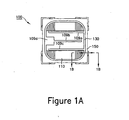
- Figure 1A shows a top view of a semiconductor device according to an embodiment of the invention.
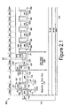
- Figure 1B shows a cross sectional side view of a portion of the semiconductor device of Figure 1A and in particular, shows a termination region according to an embodiment of the invention.
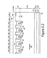
- Figure 2 shows a cross sectional side view of a portion of the semiconductor device of Figure 1A and in particular, shows an alternative termination region according to another embodiment of the invention.
- device 100 includes a trench type termination region 150 according to an embodiment of the invention. Termination region 150 is suitable for high voltage blocking devices.
- device 100 is a SiC JFET transistor. Nonetheless, trench termination 150 of the present invention is not limited to JFET transistors and may also be applied to other SiC trench devices including rectifiers (diodes) and transistors other than JFET transistors.
- device 100 includes a SiC body 102, which may be N doped.
- body 102 includes a substrate 103, an epitaxially (Epi) buffer region 104, and an Epi drift layer 105, which may have a doping concentration of about 7E15/cm 3 .
- active area 110 and termination region 150 are formed along the top surface of body 102 along the top surface of body 102 along the top surface of body 102 along active area 110 and termination region 150, which extends around the outer periphery of device 100 and surrounds active area 110.
- a gate runner/bus 130 may be disposed between active area 110 and termination region 150.
- Active area 110 includes a plurality of gate trenches 112 formed within the top surface of body 102 and extending into Epi layer 105.
- a mesa region, such as region 116, is disposed between each adjacent pair of gate trenches.
- a conventional contact metal 107 such as aluminum, that forms a source electrode.
- a highly doped region 118 of N+ conductivity that forms an ohmic contact between the Epi layer and source electrode.
- region 118 may be doped with phosphorous at a concentration of about 2E19/cm 3 and may have a thickness of about 0.5um.
- Each gate trench 112 has an implant region 114 of P+ conductivity that is formed within Epi layer 105 along the sidewalls and bottom surface of the trench.
- the doping concentration and thickness of implant region 114 along these two regions may vary.
- region 114 may have a doping concentration of about 1E19/cm 3 and a thickness of about 0.65um along the trench bottom and may have a doping concentration of about SE17/cm 3 and a thickness of about 0.3um along the trench sidewalls.
- Formed at the bottom of each gate trench 112 is a gate electrode 108 that is contacted by a metal electrode.
- gate electrodes 108 may be formed of P doped polysilicon, such as polysilicon doped with boron at a concentration of about 1E20. As shown, each gate electrode 108 may be spaced from the trench sidewall that forms mesa region 116.
- body 102 Along the bottom surface of body 102 is a conventional contact metal 106 that forms a drain electrode.
- gate runner 130 extends around the outer periphery of active area 110 and connects gate electrodes 108 to one another. Nonetheless, mechanisms other than gate runner 130 may be used to contact/connect the gate electrodes. Similarly, other transistor configurations may not require gate runner 130.
- gate runner 130 is not present when the device is a rectifier, for example. When gate runner 130 is not present, active area 110 is directly linked to termination region 150.
- gate runner 130 includes a single trench 132 formed within the top surface of body 102 and extending into Epi layer 105. Trench 132 may extend to the same depth into Epi layer 105 as gate trenches 112. Gate runner 130 also includes a mesa region 138 disposed between trench 132 and the outermost gate trench 112b of active area 110. Formed on the top surface of mesa region 138 and within Epi layer 105 is a highly doped region 146 ofN+ conductivity. As an example, region 146 may be doped with phosphorous at a concentration of about 2E19/cm 3 and may have a thickness of about 0.5um.
- Implant region 134 of P+ conductivity is formed within Epi layer 105 along the sidewalls and bottom surface of trench 132.
- Implant region 134 may have the same doping concentration and thickness configuration along the trench sidewalls and bottom surface as implant region 114.
- conductive bodies 136 are Formed in each corner of trench 132, along a portion of the sidewalls and bottom surface, are conductive bodies 136.
- conductive bodies 136 may be P doped polysilicon and in particular, may be polysilicon doped with boron at a concentration of about 1E20.
- SiO 2 silicon dioxide
- gate runner 130 is connected to a gate contact 109 of device 100.
- Gate contact 109 may be configured as a pad 109d and a plurality of gate fingers 109a-109c. This configuration of a gate pad and gate fingers increases the contact area of the gate and reduces gate resistance, for example.
- the JFET transistor of device 100 operates as follows.
- a channel region 118 exists along each mesa region 116.
- a bias voltage between gate electrode 109 and source electrode 107 is varied, thereby pinching/depleting channel region 118 and prohibiting the flow of current between drain electrode 106 and source electrode 107 or opening/undepleting channel region 118 and allowing a vertical conduction current to flow along the channel region between the electrodes.
- termination region 150 extends around the outer periphery of device 100 and surrounds gate runner 130 and active area 110.
- termination region 150 includes termination trench 152 formed within the top surface of body 102 and extending into Epi layer 105.
- termination trench 152 extends to the same depth within Epi layer 105 as the trenches formed in active area 110, in this case, gate trenches 112.
- the gate trenches and termination trench may have a depth of about 2um.
- the width of termination trench 152 may vary from about 5um to about 100um without affecting the blocking capability of device 100. Nonetheless, one skilled in the art will recognize that a smaller width for termination trench 152 allows for a larger active area 110 without having to change the size of device 100.
- Termination region 150 also includes an end mesa region 166 and a linking mesa region 164.
- End mesa region 166 forms the outer sidewall 152b of the termination trench and extends towards the outer peripheral edge of device 100.
- Linking mesa region 164 forms the inner sidewall 152a of termination trench 152 and is thereby disposed between the termination trench and the active area, linking termination region 150 to the active area.
- mesa region 164 forms the outer sidewall of trench 132.
- mesa region 164 forms the outer sidewall of the outermost trench of active area 110, in this case, gate trench 112b.
- the width of mesa region 164 needs to be well targeted for ensuring the right potential spread along termination region 150.
- the width of mesa region 164 is preferably about 2um. Nonetheless, the width of mesa region 164 may vary from about 1 um to about 4um depending on the required blocking voltage and the configuration of body 102, for example.
- An implant region of P+ conductivity is formed within Epi layer 105 along the sidewalls and bottom surface of termination trench 152, thereby surrounding the trench with a P-N junction and forming guard ring 154.
- Guard ring 154 may have the same doping concentration and thickness configuration along the trench sidewalls and bottom surface as implant region 114 formed along gate trenches 112, as described above.
- Termination region 150 also includes field insulation body 162 formed of silicon dioxide, for example.
- This insulation body is disposed over the bottom surface of trench 152 and over the top and side surfaces of conductive bodies 156 and extends along the top surface of mesa region 164 and along a portion of the top surface of mesa region 166.
- field insulation body 162 is integral with insulation layer 140 when gate runner 130 is present.
- Field insulation body 162 covers the entire outer surface of termination trench 152, thereby insulating the trench from contact and forming a floating trench.
- the thickness of field insulation body 162 may vary and in particular, is configured based on the required blocking voltage of the device. As an example, for a required blocking voltage of about 600V, field insulation body 162 is preferably about 1um thick.
- Termination region 150 may also include field plate 160 formed atop field insulation body 162. As shown, field plate 160 extends along a portion of termination trench 152 and outward beyond the outer sidewall 152b of the trench and over mesa region 166. Field plate 160 may be formed of aluminum, although other contact metals may be used. Although not required, field plate 160 is preferable in that it is useful for better spreading the depletion along termination region 150. More specifically, when field plate 160 is not present, a potential line crowding may form at the outer sidewall 152b of termination trench 152, thereby leading to a high spotty electric field and premature breakdown. Field plate 160 acts to spread the potential along this area. As an example, including field plate 160 in termination region 150 provides for about an 8% to 10% higher breakdown voltage. Preferably, field plate 160 has a minimum width of 5um and may be increased depending on the required breakdown voltage of the device.
- field plate 160 is insulated from termination trench 152 by field insulation body 162 and is shorted to either the source electrode or gate electrode of the device, thereby placing the field plate at the same potential as the source or gate.
- field plate 160 is not shorted to either the source or gate but rather, is a floating field plate.
- field plate 160 contacts guard ring 154 through an opening formed in field insulation body 162.
- one opening is formed in field insulation body 162 at each corner of device 100 to create this connection.
- Termination region 150 may be ended by a highly doped region 158 of N+ conductivity formed within the top surface of Epi layer 105 along mesa region 166 along the outer peripheral edge of device 100.
- region 158 may be phosphorous doped at a concentration of about 2E19/cm 3 and may have a thickness of about 0.5um.
- Region 158 functions as an equipotential ring (EQR), or in other words, as a channel stopper. Nonetheless, this channel stop function is not as critical as in silicon devices and as such, EQR 158 is not required.
- termination region 150 may be adapted to devices that require blocking voltages other than 600V.
- FIG. 2 there is shown a cross sectional side view of a portion of a device 200 according to another embodiment of the invention (note that the dimensions shown in Figure 2 are for example purposes only and that device 200 is not drawn to scale).
- Device 200 includes an alternative trench termination 250 according to another embodiment of the invention.
- device 200 is a SiC JFET transistor and resembles device 100 as shown in Figures 1A and 1B except for the difference in terminations. Note that Figure 2 shows the same cross sectional view as Figure 1B .
- termination 250 may also be applied to other SiC trench devices, including rectifiers and transistors other than JFET transistors.
- device 200 includes a SiC body 102 that has an active area 110, gate runner/bus 230, and termination region 250 formed therein.
- Active area 110 is as described above.
- Gate runner 230 is similar to gate runner 130 and extends around the outer periphery of active area 110, connecting the gate electrodes 108 of the device to a common gate contact 109. Again, mechanisms other than gate runner 230 may be used to contact/connect the gate contacts and gate runner 230 is not required, such as when the device is a rectifier, for example.
- active area 110 is directly linked to termination region 250.
- gate runner 230 includes a single trench 232 that may extend to the same depth into Epi layer 105 as gate trenches 112. Gate runner 230 also includes a mesa region 238 disposed between trench 232 and the outermost gate trench 112b of active area 110. Formed along the top surface of mesa region 238 within Epi layer 105 is a highly doped region 246 ofN+ conductivity. As an example, region 246 may be phosphorous doped at a concentration of about 2E19/cm 3 and may have a thickness of about 0.5um. An implant region 234 of P+ conductivity is formed within Epi layer 105 along the sidewalls and bottom surface of trench 232.
- implant region 234 may vary along the trench sidewalls and bottom surface as similarly described above and in particular, may resemble the configuration of implant region 114 formed along gate trenches 112.
- An insulation layer 240 formed of silicon dioxide, for example, is disposed over the sidewalls and bottom surface of trench 232 and extends along the top surface of mesa region 238. Similar to above, insulation layer 240 is part of field insulation body 262 within termination region 250 and as such, may have a thickness consistent with that of field insulation body 262.
- An opening 242 is formed in insulation layer 240 down to the bottom surface of trench 232, thereby exposing implant region 234.
- a gate electrode 244 made of a metal, such as aluminum, is formed within opening 242 and contacts the gate electrodes 108 of the device.
- termination 250 similar to termination region 150, this region extends around the outer periphery of device 200 and surrounds gate runner 230 and active area 110.
- termination 250 includes a plurality (i.e., two or more) of termination trenches 252a-i formed within the top surface of body 102 and extending into Epi layer 105. Each pair of adjacent trenches is separated by a mesa region 264.
- termination trenches 252 extend to the same depth within Epi layer 105 as the trenches formed in active area 110, in this case, gate trenches 112.
- the termination and gate trenches may have a depth of about 2um.
- the width of termination trenches 252 may vary and does not affect the blocking capability of device 200. In general, the trench width is largely determined by the available technology used to form the trenches. As an example, trenches 252 may have a width of about 3um. Overall, the number of termination trenches may vary and in particular, is configured based on the desired voltage to be blocked, as well as the width of mesa regions 264. Note that each of mesa regions 264 may have substantially the same width, or the widths may vary among the mesa regions.
- Termination region 250 also includes end mesa region 266 and linking mesa region 263.
- End mesa region 266 forms the outer sidewall of the outermost termination trench 252i and extends towards the outer peripheral edge of device 200.
- Linking mesa region 263 forms the inner sidewall of the inner most termination trench 252a and is thereby disposed between the termination trenches and the active area, linking termination region 250 to the active area.
- mesa region 263 forms the outer sidewall of trench 232.
- mesa region 263 forms the outer sidewall of the outermost trench of active area 110, in this case, gate trench 112b.
- the width of mesa region 263 needs to be well targeted for ensuring the right potential spread along termination region 250.
- the width of mesa region 263 is preferably about 2um. Nonetheless, the width of mesa region 263 may vary and may wider than 2um, for example, depending on the required blocking voltage and the configuration of body 102, for example.
- An implant region of P+ conductivity is formed within Epi layer 105 along the sidewalls and bottom surface of each of the termination trenches 252, thereby surrounding each trench with a P-N junction and forming a plurality of guard rings 254.
- the doping concentration and thickness configuration of each guard ring 254 may vary along the trench sidewalls and bottom surface as similarly described above and in particular, may resemble the configuration of implant region 114 formed along gate trenches 112, as described above.
- a conductive body 256 Formed within each of the termination trenches 252 is a conductive body 256 that fills a portion of the trench.
- These conductive bodies may be P doped polysilicon and in particular, may be polysilicon doped with boron at a concentration of about 1E20, for example. Nonetheless, similar to termination trench 152, termination trenches 252 are insulated and thereby floating, as discussed below.
- Termination region 250 also includes field insulation body 262 formed of silicon dioxide, for example. This insulation body is disposed over each of the termination trenches 252, filling the remaining portion of each trench, and extends along the top surface of mesa region 263, along the top surfaces of mesa regions 264, and along a portion of the top surface of mesa region 266. As shown, field insulation body 262 is integral with insulation layer 240 when gate runner 230 is present. Field insulation body 262 covers the entire outer surface of termination trenches 252, thereby insulating the trenches from contact and forming floating trenches. The thickness of field insulation body 262 may vary from about 5000A to several microns and in particular, is configured based on the required blocking voltage of the device. As an example, for a required blocking voltage of about 600V, field insulation body 162 is preferably about 1um thick.
- termination region 250 may also include a field plate (not shown in Figure 2 ) formed atop field insulation body 262. This field plate extends along a portion of termination region 250 and outward beyond the outer sidewall of the outermost termination trench 252i and over mesa region 266.
- the field plate may be formed of aluminum, although other contact metals may be used.
- the field plate of termination region 250 is not required but is preferred in that it provides for a higher breakdown voltage as compared to when the field plate is not included.
- the field plate of termination region 250 may be insulated from the termination trenches by field insulation body 262 and shorted to either the source electrode or gate electrode of the device.
- Termination region 250 may also include an N+ doped EQR 258 formed along mesa region 266 along the outer peripheral edge of device 200, which EQR functions as a channel stopper.
- region 258 may be phosphorous doped at a concentration of about 2E19/cm 3 and may have a thickness of about 0.5um.
- termination region 250 may be adapted to devices that require blocking voltages other than 600V by varying, for example, the width of mesa region 263, the thickness of field insulation layer 262, and the number of termination trenches 252.
Landscapes
- Junction Field-Effect Transistors (AREA)
- Electrodes Of Semiconductors (AREA)
- Bipolar Transistors (AREA)
Claims (25)
- Dispositif semi-conducteur (100, 200) comprenant un corps (102) ayant des première et deuxième surfaces majeures opposées, une zone active (110) formée le long de ladite première surface majeure dudit corps (102), une région de terminaison (150, 250) formée le long de ladite première surface majeure dudit corps (102) et définissant ladite zone active (110), ladite région de terminaison (150, 250) incluant une tranchée de terminaison (252) formée dans ledit corps (102) et ayant des parois latérales et une surface de fond, une bague de protection (254) réalisée dans ledit corps (102) le long desdites parois latérales et de ladite surface de fond de ladite tranchée de terminaison (252), et un corps d'isolation de champ (262) couvrant ladite tranchée de terminaison (252), ledit dispositif semi-conducteur (100, 200) étant caractérisé en ce que:ledit corps (102) est un corps en carbure de silicium;où ledit dispositif semi-conducteur (100, 200) comprend en outre un corps conducteur (256) disposé dans ladite tranchée de terminaison (252) sous ledit corps d'isolation de champ (262).
- Dispositif semi-conducteur (100, 200) selon la revendication 1, comprenant en outre une plaque de champ (160) disposée sur ledit corps d'isolation de champ (262).
- Dispositif semi-conducteur (100, 200) selon la revendication 2, dans lequel ladite plaque de champ (160) s'étend au-delà d'une paroi latérale extérieure de ladite tranchée de terminaison (252).
- Dispositif semi-conducteur (100, 200) selon la revendication 2, dans lequel ladite plaque de champ (160) est flottante.
- Dispositif semi-conducteur (100, 200) selon la revendication 4, dans lequel ledit corps d'isolation de champ (262) possède une ouverture formée dans celui-ci, et où ladite plaque champ (160) s'étend à travers ladite ouverture et vient en contact avec ladite bague de protection (254).
- Dispositif semi-conducteur (100, 200) selon la revendication 2, dans lequel ladite plaque de champ (160) est court-circuitée à une électrode dudit dispositif (100, 200).
- Dispositif semi-conducteur (100, 200) selon la revendication 1, dans lequel ladite région de terminaison (150, 250) comprend en outre une région mésa (263, 264, 266) disposée entre ladite tranchée de terminaison (252) et ladite zone active (110), ladite région mésa (263, 264, 266) reliant ladite région de terminaison (150, 250) à ladite zone active (110).
- Dispositif semi-conducteur (100, 200) selon la revendication 7, dans lequel ledit corps d'isolation de champ (262) s'étend sur une surface supérieure de ladite région mésa (263, 264, 266).
- Dispositif semi-conducteur (100, 200) selon la revendication 1, dans lequel ladite région de terminaison (150, 250) comprend en outre une bague EQR (258) formée le long d'un bord périphérique extérieur dudit dispositif (100, 200).
- Dispositif semi-conducteur (100, 200) selon la revendication 1, dans lequel ladite zone active (110) comprend au moins une tranchée (252) réalisée dans ledit corps en carbure de silicium.
- Dispositif semi-conducteur (100, 200) selon la revendication 10, dans lequel ladite tranchée de terminaison (252) et ladite au moins une tranchée (252) de ladite zone active (110) s'étendent sur environ la même profondeur dans ledit corps en carbure de silicium.
- Dispositif semi-conducteur (100, 200) selon la revendication 1, dans lequel ledit corps conducteur (256) est en polysilicium dopé.
- Dispositif semi-conducteur (100, 200) selon la revendication 1, dans lequel ledit dispositif semi-conducteur (100, 200) est un transistor JFET.
- Dispositif semi-conducteur (100, 200) selon la revendication 13, comprenant en outre un canal de porte disposé entre ladite tranchée de terminaison (252) et ladite zone active (110).
- Dispositif semi-conducteur (100, 200) selon la revendication 1, dans lequel ladite région de terminaison (150, 250) comporte une pluralité de tranchées de terminaison (252) formées dans ledit corps en carbure de silicium, chaque tranchée de terminaison (252) ayant des parois latérales et une surface de fond et étant espacée d'une tranchée de terminaison adjacente (252) par une région mésa (263, 264, 266).
- Dispositif semi-conducteur (100, 200) selon la revendication 15, dans lequel chacune de ladite pluralité de tranchées de terminaison (252) comprend une bague de protection (254) formée dans ledit corps en carbure de silicium le long desdites parois latérales et de ladite surface de fond de ladite tranchée de terminaison (252).
- Dispositif semi-conducteur (100, 200) selon la revendication 16, dans lequel chaque corps d'isolation de champ (262) couvre chacune de ladite pluralité de tranchées de terminaison (252).
- Dispositif semi-conducteur (100, 200) selon la revendication 17, comprenant en outre une plaque de champ (160) disposée sur ledit corps d'isolation de champ (262).
- Dispositif semi-conducteur (100, 200) selon la revendication 18, comprenant en outre un corps conducteur (256) disposé dans chacune desdites tranchées de terminaison (252) et sous ledit corps d'isolation de champ (262).
- Dispositif semi-conducteur (100, 200) selon la revendication 19, où lesdits corps conducteurs (256) sont en polysilicium dopé.
- Dispositif semi-conducteur (100, 200) selon la revendication 18, dans lequel ladite région de terminaison (150, 250) comprend en outre une région de liaison mésa (263, 264, 266) qui relie ladite région de terminaison (150, 250) à ladite zone active (110).
- Dispositif semi-conducteur (100, 200) selon la revendication 18, dans lequel ladite région de terminaison (150, 250) comprend en outre une bague EQR (258) formée le long d'un bord périphérique extérieur dudit dispositif (100).
- Dispositif semi-conducteur (100, 200) selon la revendication 16, dans lequel ladite zone active (110) comprend au moins une tranchée (252) formée dans ledit corps en carbure de silicium.
- Dispositif semi-conducteur (100, 200) selon la revendication 23, dans lequel chacune desdites tranchées de terminaison (252) et ladite au moins une tranchée (252) de ladite zone active (110) s'étendent sur environ la même profondeur dans ledit corps en carbure de silicium.
- Dispositif semi-conducteur (100, 200) selon la revendication 16, dans lequel ledit dispositif semi-conducteur (100, 200) est un transistor JFET.
Applications Claiming Priority (2)
| Application Number | Priority Date | Filing Date | Title |
|---|---|---|---|
| US65878905P | 2005-03-04 | 2005-03-04 | |
| US11/365,291 US9419092B2 (en) | 2005-03-04 | 2006-03-01 | Termination for SiC trench devices |
Publications (3)
| Publication Number | Publication Date |
|---|---|
| EP1699083A2 EP1699083A2 (fr) | 2006-09-06 |
| EP1699083A3 EP1699083A3 (fr) | 2009-01-07 |
| EP1699083B1 true EP1699083B1 (fr) | 2011-09-07 |
Family
ID=36570285
Family Applications (1)
| Application Number | Title | Priority Date | Filing Date |
|---|---|---|---|
| EP06004364A Expired - Lifetime EP1699083B1 (fr) | 2005-03-04 | 2006-03-03 | Terminaison pour dispositifs en tranchée en SiC. |
Country Status (4)
| Country | Link |
|---|---|
| US (1) | US9419092B2 (fr) |
| EP (1) | EP1699083B1 (fr) |
| JP (1) | JP5199544B2 (fr) |
| AT (1) | ATE523899T1 (fr) |
Cited By (1)
| Publication number | Priority date | Publication date | Assignee | Title |
|---|---|---|---|---|
| EP4345911A1 (fr) * | 2022-09-06 | 2024-04-03 | Infineon Technologies Austria AG | Transistor vertical à effet de champ à jonction comprenant une pluralité de régions mesa |
Families Citing this family (34)
| Publication number | Priority date | Publication date | Assignee | Title |
|---|---|---|---|---|
| US7394158B2 (en) | 2004-10-21 | 2008-07-01 | Siliconix Technology C.V. | Solderable top metal for SiC device |
| US7812441B2 (en) | 2004-10-21 | 2010-10-12 | Siliconix Technology C.V. | Schottky diode with improved surge capability |
| US7834376B2 (en) | 2005-03-04 | 2010-11-16 | Siliconix Technology C. V. | Power semiconductor switch |
| US8368165B2 (en) | 2005-10-20 | 2013-02-05 | Siliconix Technology C. V. | Silicon carbide Schottky diode |
| WO2008016619A1 (fr) | 2006-07-31 | 2008-02-07 | Vishay-Siliconix | Métal barrière de molybdène pour une diode schottky de sic et son procédé de fabrication |
| DE102006046853B4 (de) | 2006-10-02 | 2010-01-07 | Infineon Technologies Austria Ag | Randkonstruktion für ein Halbleiterbauelement und Verfahren zur Herstellung derselben |
| US9484451B2 (en) * | 2007-10-05 | 2016-11-01 | Vishay-Siliconix | MOSFET active area and edge termination area charge balance |
| US9117739B2 (en) * | 2010-03-08 | 2015-08-25 | Cree, Inc. | Semiconductor devices with heterojunction barrier regions and methods of fabricating same |
| US20160372542A9 (en) * | 2011-07-19 | 2016-12-22 | Yeeheng Lee | Termination of high voltage (hv) devices with new configurations and methods |
| US8803251B2 (en) * | 2011-07-19 | 2014-08-12 | Alpha And Omega Semiconductor Incorporated | Termination of high voltage (HV) devices with new configurations and methods |
| US8680587B2 (en) | 2011-09-11 | 2014-03-25 | Cree, Inc. | Schottky diode |
| JP5865016B2 (ja) * | 2011-10-31 | 2016-02-17 | 株式会社 日立パワーデバイス | トレンチ型ショットキー接合型半導体装置及びその製造方法 |
| US9431249B2 (en) | 2011-12-01 | 2016-08-30 | Vishay-Siliconix | Edge termination for super junction MOSFET devices |
| US20130168765A1 (en) * | 2012-01-04 | 2013-07-04 | Vishay General Semiconductor Llc | Trench dmos device with improved termination structure for high voltage applications |
| US9614043B2 (en) | 2012-02-09 | 2017-04-04 | Vishay-Siliconix | MOSFET termination trench |
| US9842911B2 (en) | 2012-05-30 | 2017-12-12 | Vishay-Siliconix | Adaptive charge balanced edge termination |
| EP2893566B1 (fr) | 2012-09-05 | 2016-05-18 | Institut National des Sciences Appliquées de Lyon | Procede de fabrication d'un transistor a effet de champ a jonction jfet |
| JP6135364B2 (ja) * | 2013-07-26 | 2017-05-31 | 住友電気工業株式会社 | 炭化珪素半導体装置およびその製造方法 |
| DE102014103540B4 (de) | 2014-03-14 | 2020-02-20 | Infineon Technologies Austria Ag | Halbleiterbauelement und integrierte schaltung |
| US9508596B2 (en) | 2014-06-20 | 2016-11-29 | Vishay-Siliconix | Processes used in fabricating a metal-insulator-semiconductor field effect transistor |
| US9887259B2 (en) | 2014-06-23 | 2018-02-06 | Vishay-Siliconix | Modulated super junction power MOSFET devices |
| KR102098996B1 (ko) | 2014-08-19 | 2020-04-08 | 비쉐이-실리코닉스 | 초접합 금속 산화물 반도체 전계 효과 트랜지스터 |
| WO2016080322A1 (fr) | 2014-11-18 | 2016-05-26 | ローム株式会社 | Dispositif à semi-conducteur et procédé de fabrication de dispositif à semi-conducteur |
| US10396215B2 (en) | 2015-03-10 | 2019-08-27 | United Silicon Carbide, Inc. | Trench vertical JFET with improved threshold voltage control |
| US20170018657A1 (en) | 2015-07-14 | 2017-01-19 | United Silicon Carbide, Inc. | Vertical jfet made using a reduced mask set |
| US10050154B2 (en) | 2015-07-14 | 2018-08-14 | United Silicon Carbide, Inc. | Trench vertical JFET with ladder termination |
| WO2018132458A1 (fr) * | 2017-01-13 | 2018-07-19 | United Silicon Carbide, Inc. | Jfet vertical à tranchées avec terminaison d'échelle |
| DE112017007040T5 (de) * | 2017-02-10 | 2019-10-24 | Mitsubishi Electric Corporation | Halbleitereinheit |
| JP7247892B2 (ja) * | 2017-12-15 | 2023-03-29 | 住友電気工業株式会社 | 炭化珪素半導体装置 |
| WO2019170631A1 (fr) * | 2018-03-06 | 2019-09-12 | Abb Schweiz Ag | Dispositif à semi-conducteur de forte puissance à plaque de champ et structure de terminaison mésa auto-alignées et son procédé de fabrication |
| JP7685503B2 (ja) * | 2020-07-31 | 2025-05-29 | ローム株式会社 | SiC半導体装置 |
| JP2024046022A (ja) * | 2022-09-22 | 2024-04-03 | 富士電機株式会社 | 半導体装置 |
| KR20250158300A (ko) * | 2024-04-30 | 2025-11-06 | 삼성전자주식회사 | 반도체 소자 |
| EP4668340A1 (fr) * | 2024-06-17 | 2025-12-24 | Infineon Technologies Austria AG | Transistor à effet de champ à jonction verticale comprenant une couche de silicium dans une structure de tranchée |
Family Cites Families (161)
| Publication number | Priority date | Publication date | Assignee | Title |
|---|---|---|---|---|
| JPS51132779A (en) | 1975-05-14 | 1976-11-18 | Hitachi Ltd | Production method of vertical-junction type field-effect transistor |
| US4206540A (en) * | 1978-06-02 | 1980-06-10 | International Rectifier Corporation | Schottky device and method of manufacture using palladium and platinum intermetallic alloys and titanium barrier |
| JPS60201666A (ja) * | 1984-03-27 | 1985-10-12 | Nec Corp | 半導体装置 |
| FR2579023B1 (fr) | 1985-03-12 | 1988-06-24 | Silicium Semiconducteur Ssc | Composant semiconducteur a tenue en tension amelioree par sillons peripheriques multiples |
| JPH0669040B2 (ja) * | 1985-05-13 | 1994-08-31 | 株式会社東芝 | 光半導体装置 |
| US4648175A (en) * | 1985-06-12 | 1987-03-10 | Ncr Corporation | Use of selectively deposited tungsten for contact formation and shunting metallization |
| JPS6271271A (ja) * | 1985-09-24 | 1987-04-01 | Sharp Corp | 炭化珪素半導体の電極構造 |
| US5003372A (en) * | 1988-06-16 | 1991-03-26 | Hyundai Electronics Industries Co., Ltd. | High breakdown voltage semiconductor device |
| EP0360036B1 (fr) * | 1988-09-20 | 1994-06-01 | Siemens Aktiengesellschaft | Jonction pn plane à tenue en tension élévée |
| US5047833A (en) * | 1990-10-17 | 1991-09-10 | International Rectifier Corporation | Solderable front metal contact for MOS devices |
| US5322812A (en) * | 1991-03-20 | 1994-06-21 | Crosspoint Solutions, Inc. | Improved method of fabricating antifuses in an integrated circuit device and resulting structure |
| US5233215A (en) * | 1992-06-08 | 1993-08-03 | North Carolina State University At Raleigh | Silicon carbide power MOSFET with floating field ring and floating field plate |
| US5362975A (en) * | 1992-09-02 | 1994-11-08 | Kobe Steel Usa | Diamond-based chemical sensors |
| US5384470A (en) * | 1992-11-02 | 1995-01-24 | Kobe Steel, Usa, Inc. | High temperature rectifying contact including polycrystalline diamond and method for making same |
| US6040617A (en) | 1992-12-22 | 2000-03-21 | Stmicroelectronics, Inc. | Structure to provide junction breakdown stability for deep trench devices |
| US5323040A (en) * | 1993-09-27 | 1994-06-21 | North Carolina State University At Raleigh | Silicon carbide field effect device |
| JPH07302896A (ja) * | 1994-04-28 | 1995-11-14 | Ngk Insulators Ltd | 半導体装置およびその製造方法 |
| DE4423068C1 (de) * | 1994-07-01 | 1995-08-17 | Daimler Benz Ag | Feldeffekt-Transistoren aus SiC und Verfahren zu ihrer Herstellung |
| TW286435B (fr) * | 1994-07-27 | 1996-09-21 | Siemens Ag | |
| JPH0897441A (ja) * | 1994-09-26 | 1996-04-12 | Fuji Electric Co Ltd | 炭化けい素ショットキーダイオードの製造方法 |
| JP3272242B2 (ja) | 1995-06-09 | 2002-04-08 | 三洋電機株式会社 | 半導体装置 |
| JPH0936393A (ja) | 1995-07-25 | 1997-02-07 | Denso Corp | ショットキー接合を有する半導体装置の製造方法 |
| US5689128A (en) * | 1995-08-21 | 1997-11-18 | Siliconix Incorporated | High density trenched DMOS transistor |
| US5967795A (en) * | 1995-08-30 | 1999-10-19 | Asea Brown Boveri Ab | SiC semiconductor device comprising a pn junction with a voltage absorbing edge |
| US6573534B1 (en) * | 1995-09-06 | 2003-06-03 | Denso Corporation | Silicon carbide semiconductor device |
| WO1997027626A1 (fr) | 1996-01-26 | 1997-07-31 | The Whitaker Corporation | Boitier de circuit integre a dissipation calorifique et mise a la masse ameliorees |
| US5929523A (en) * | 1996-03-07 | 1999-07-27 | 3C Semiconductor Corporation | Os rectifying Schottky and ohmic junction and W/WC/TiC ohmic contacts on SiC |
| US6002159A (en) * | 1996-07-16 | 1999-12-14 | Abb Research Ltd. | SiC semiconductor device comprising a pn junction with a voltage absorbing edge |
| US5801836A (en) * | 1996-07-16 | 1998-09-01 | Abb Research Ltd. | Depletion region stopper for PN junction in silicon carbide |
| US5753938A (en) * | 1996-08-08 | 1998-05-19 | North Carolina State University | Static-induction transistors having heterojunction gates and methods of forming same |
| JP3123452B2 (ja) * | 1996-12-10 | 2001-01-09 | 富士電機株式会社 | ショットキーバリアダイオード |
| SE9700156D0 (sv) * | 1997-01-21 | 1997-01-21 | Abb Research Ltd | Junction termination for Si C Schottky diode |
| JP3938964B2 (ja) * | 1997-02-10 | 2007-06-27 | 三菱電機株式会社 | 高耐圧半導体装置およびその製造方法 |
| US6441455B1 (en) * | 1997-03-06 | 2002-08-27 | International Rectifier Corporation | Low dosage field rings for high voltage semiconductor device |
| US6100572A (en) * | 1997-03-20 | 2000-08-08 | International Rectifier Corp. | Amorphous silicon combined with resurf region for termination for MOSgated device |
| US5932894A (en) * | 1997-06-26 | 1999-08-03 | Abb Research Ltd. | SiC semiconductor device comprising a pn junction |
| US20010043172A1 (en) | 1997-08-25 | 2001-11-22 | Mcgrath James M. | Field emission display |
| JPH1187698A (ja) | 1997-09-02 | 1999-03-30 | Kansai Electric Power Co Inc:The | 高耐圧半導体装置及びこの装置を用いた電力変換器 |
| JPH1187690A (ja) | 1997-09-12 | 1999-03-30 | Meidensha Corp | 半導体素子 |
| US6207591B1 (en) * | 1997-11-14 | 2001-03-27 | Kabushiki Kaisha Toshiba | Method and equipment for manufacturing semiconductor device |
| US6362495B1 (en) * | 1998-03-05 | 2002-03-26 | Purdue Research Foundation | Dual-metal-trench silicon carbide Schottky pinch rectifier |
| KR100309490B1 (ko) | 1998-05-21 | 2002-04-24 | 윤종용 | 다용도인쇄장치 |
| JP2000022178A (ja) | 1998-06-29 | 2000-01-21 | Sanyo Electric Co Ltd | ショットキーバリアダイオード |
| US6054365A (en) * | 1998-07-13 | 2000-04-25 | International Rectifier Corp. | Process for filling deep trenches with polysilicon and oxide |
| JP3988262B2 (ja) * | 1998-07-24 | 2007-10-10 | 富士電機デバイステクノロジー株式会社 | 縦型超接合半導体素子およびその製造方法 |
| US6303986B1 (en) | 1998-07-29 | 2001-10-16 | Silicon Light Machines | Method of and apparatus for sealing an hermetic lid to a semiconductor die |
| DE19840032C1 (de) | 1998-09-02 | 1999-11-18 | Siemens Ag | Halbleiterbauelement und Herstellungsverfahren dazu |
| ATE416479T1 (de) | 1998-12-18 | 2008-12-15 | Infineon Technologies Ag | Leistungshalbleiterbauelement |
| EP1064684A1 (fr) * | 1999-01-15 | 2001-01-03 | Infineon Technologies AG | Bordure terminale pour un composant a semi-conducteur, diode a barriere de schottky dotee d'une bordure terminale et procede de fabrication d'une diode a barriere de schottky |
| JP3971062B2 (ja) * | 1999-07-29 | 2007-09-05 | 株式会社東芝 | 高耐圧半導体装置 |
| DE19943143B4 (de) * | 1999-09-09 | 2008-04-24 | Infineon Technologies Ag | Halbleiterbauelement für hohe Sperrspannungen bei gleichzeitig niedrigem Einschaltwiderstand und Verfahren zu dessen Herstellung |
| KR100462980B1 (ko) | 1999-09-13 | 2004-12-23 | 비쉐이 메저먼츠 그룹, 인코포레이티드 | 반도체장치용 칩 스케일 표면 장착 패키지 및 그 제조공정 |
| EP1222694B1 (fr) * | 1999-09-22 | 2005-02-02 | SiCED Electronics Development GmbH & Co KG | Dispositif semi-conducteur en SiC à contact Schottky et sa méthode de fabrication |
| US6703707B1 (en) * | 1999-11-24 | 2004-03-09 | Denso Corporation | Semiconductor device having radiation structure |
| US6373076B1 (en) | 1999-12-07 | 2002-04-16 | Philips Electronics North America Corporation | Passivated silicon carbide devices with low leakage current and method of fabricating |
| JP3804375B2 (ja) * | 1999-12-09 | 2006-08-02 | 株式会社日立製作所 | 半導体装置とそれを用いたパワースイッチング駆動システム |
| US6573537B1 (en) | 1999-12-22 | 2003-06-03 | Lumileds Lighting, U.S., Llc | Highly reflective ohmic contacts to III-nitride flip-chip LEDs |
| US6486499B1 (en) | 1999-12-22 | 2002-11-26 | Lumileds Lighting U.S., Llc | III-nitride light-emitting device with increased light generating capability |
| US6514782B1 (en) | 1999-12-22 | 2003-02-04 | Lumileds Lighting, U.S., Llc | Method of making a III-nitride light-emitting device with increased light generating capability |
| DE10002362A1 (de) | 2000-01-20 | 2001-08-02 | Infineon Technologies Ag | Halbleiterbauelement |
| US6699775B2 (en) * | 2000-02-22 | 2004-03-02 | International Rectifier Corporation | Manufacturing process for fast recovery diode |
| US6613671B1 (en) * | 2000-03-03 | 2003-09-02 | Micron Technology, Inc. | Conductive connection forming methods, oxidation reducing methods, and integrated circuits formed thereby |
| US6624522B2 (en) | 2000-04-04 | 2003-09-23 | International Rectifier Corporation | Chip scale surface mounted device and process of manufacture |
| US7892974B2 (en) | 2000-04-11 | 2011-02-22 | Cree, Inc. | Method of forming vias in silicon carbide and resulting devices and circuits |
| JP4240752B2 (ja) | 2000-05-01 | 2009-03-18 | 富士電機デバイステクノロジー株式会社 | 半導体装置 |
| US6509240B2 (en) * | 2000-05-15 | 2003-01-21 | International Rectifier Corporation | Angle implant process for cellular deep trench sidewall doping |
| KR100370231B1 (ko) | 2000-06-13 | 2003-01-29 | 페어차일드코리아반도체 주식회사 | 리드프레임의 배면에 직접 부착되는 절연방열판을구비하는 전력 모듈 패키지 |
| JP2002026056A (ja) | 2000-07-12 | 2002-01-25 | Sony Corp | 半田バンプの形成方法及び半導体装置の製造方法 |
| WO2002007312A2 (fr) | 2000-07-13 | 2002-01-24 | Isothermal Systems Research, Inc. | Dispositifs de commutation de puissance a semiconducteurs, convertisseurs de puissance, ensembles de circuits integres, circuits integres, procedes de commutation de courant de suite, procedes de formation d'un dispositif de commutation de puissance a semiconducteurs, procedes de conversion de puissance, procedes d'encapsul |
| JP2002118268A (ja) | 2000-10-10 | 2002-04-19 | Matsushita Electric Ind Co Ltd | 半導体素子および半導体素子への結線方法 |
| JP4843843B2 (ja) * | 2000-10-20 | 2011-12-21 | 富士電機株式会社 | 超接合半導体素子 |
| DE10052004C1 (de) * | 2000-10-20 | 2002-02-28 | Infineon Technologies Ag | Vertikaler Feldeffekttransistor mit Kompensationszonen und Anschlüssen an einer Seite eines Halbleiterkörpers |
| FR2816113A1 (fr) * | 2000-10-31 | 2002-05-03 | St Microelectronics Sa | Procede de realisation d'une zone dopee dans du carbure de silicium et application a une diode schottky |
| JP2002158363A (ja) | 2000-11-17 | 2002-05-31 | Matsushita Electric Ind Co Ltd | ショットキバリアダイオードの電極構造 |
| JP4088033B2 (ja) * | 2000-11-27 | 2008-05-21 | 株式会社東芝 | 半導体装置 |
| US6573128B1 (en) * | 2000-11-28 | 2003-06-03 | Cree, Inc. | Epitaxial edge termination for silicon carbide Schottky devices and methods of fabricating silicon carbide devices incorporating same |
| US6713813B2 (en) * | 2001-01-30 | 2004-03-30 | Fairchild Semiconductor Corporation | Field effect transistor having a lateral depletion structure |
| JP4286465B2 (ja) | 2001-02-09 | 2009-07-01 | 三菱電機株式会社 | 半導体装置とその製造方法 |
| DE10205345B9 (de) * | 2001-02-09 | 2007-12-20 | Fuji Electric Co., Ltd., Kawasaki | Halbleiterbauelement |
| GB0104342D0 (en) * | 2001-02-22 | 2001-04-11 | Koninkl Philips Electronics Nv | Semiconductor devices |
| JP4872158B2 (ja) | 2001-03-05 | 2012-02-08 | 住友電気工業株式会社 | ショットキーダイオード、pn接合ダイオード、pin接合ダイオード、および製造方法 |
| US7087997B2 (en) * | 2001-03-12 | 2006-08-08 | International Business Machines Corporation | Copper to aluminum interlayer interconnect using stud and via liner |
| US7119447B2 (en) | 2001-03-28 | 2006-10-10 | International Rectifier Corporation | Direct fet device for high frequency application |
| EP1265295A3 (fr) * | 2001-06-04 | 2004-05-12 | Matsushita Electric Industrial Co., Ltd. | Diode Schottky en carbure de silicium et procédé pour sa fabrication |
| US6764906B2 (en) * | 2001-07-03 | 2004-07-20 | Siliconix Incorporated | Method for making trench mosfet having implanted drain-drift region |
| US6621122B2 (en) * | 2001-07-06 | 2003-09-16 | International Rectifier Corporation | Termination structure for superjunction device |
| US20030030051A1 (en) * | 2001-08-09 | 2003-02-13 | International Rectifier Corporation | Superjunction device with improved avalanche capability and breakdown voltage |
| JP4602609B2 (ja) | 2001-08-28 | 2010-12-22 | 東芝キヤリア株式会社 | 空気調和機 |
| JP4288907B2 (ja) * | 2001-08-29 | 2009-07-01 | 株式会社デンソー | 炭化珪素半導体装置及びその製造方法 |
| US6855981B2 (en) * | 2001-08-29 | 2005-02-15 | Denso Corporation | Silicon carbide power device having protective diode |
| JP2003124437A (ja) | 2001-10-19 | 2003-04-25 | Mitsubishi Electric Corp | 半導体装置 |
| US20040262685A1 (en) | 2001-11-01 | 2004-12-30 | Zingg Rene Paul | Thin film lateral soi power device |
| US6828609B2 (en) * | 2001-11-09 | 2004-12-07 | Infineon Technologies Ag | High-voltage semiconductor component |
| JP3891838B2 (ja) | 2001-12-26 | 2007-03-14 | 株式会社ルネサステクノロジ | 半導体装置およびその製造方法 |
| DE10164494B9 (de) * | 2001-12-28 | 2014-08-21 | Epcos Ag | Verkapseltes Bauelement mit geringer Bauhöhe sowie Verfahren zur Herstellung |
| WO2003065459A1 (fr) * | 2002-01-28 | 2003-08-07 | Mitsubishi Denki Kabushiki Kaisha | Dispositif a semi-conducteur |
| JP4126915B2 (ja) * | 2002-01-30 | 2008-07-30 | 富士電機デバイステクノロジー株式会社 | 半導体装置 |
| GB0202437D0 (en) * | 2002-02-02 | 2002-03-20 | Koninkl Philips Electronics Nv | Cellular mosfet devices and their manufacture |
| US6622380B1 (en) * | 2002-02-12 | 2003-09-23 | Micron Technology, Inc. | Methods for manufacturing microelectronic devices and methods for mounting microelectronic packages to circuit boards |
| US6693308B2 (en) * | 2002-02-22 | 2004-02-17 | Semisouth Laboratories, Llc | Power SiC devices having raised guard rings |
| JP4126359B2 (ja) | 2002-03-01 | 2008-07-30 | 新電元工業株式会社 | 炭化けい素ショットキーダイオードおよびその製造方法 |
| JP4051971B2 (ja) * | 2002-03-15 | 2008-02-27 | 株式会社デンソー | 炭化珪素半導体装置およびその製造方法 |
| US6855970B2 (en) * | 2002-03-25 | 2005-02-15 | Kabushiki Kaisha Toshiba | High-breakdown-voltage semiconductor device |
| US7262434B2 (en) * | 2002-03-28 | 2007-08-28 | Rohm Co., Ltd. | Semiconductor device with a silicon carbide substrate and ohmic metal layer |
| JP3890311B2 (ja) | 2002-03-28 | 2007-03-07 | ローム株式会社 | 半導体装置およびその製造方法 |
| JP3828036B2 (ja) | 2002-03-28 | 2006-09-27 | 三菱電機株式会社 | 樹脂モールド型デバイスの製造方法及び製造装置 |
| EP1351298B1 (fr) | 2002-03-28 | 2007-12-26 | Infineon Technologies AG | Procédé de production d'une plaquette à semiconducteur |
| JP3993458B2 (ja) * | 2002-04-17 | 2007-10-17 | 株式会社東芝 | 半導体装置 |
| JP2004079988A (ja) | 2002-06-19 | 2004-03-11 | Toshiba Corp | 半導体装置 |
| US7064637B2 (en) | 2002-07-18 | 2006-06-20 | Wispry, Inc. | Recessed electrode for electrostatically actuated structures |
| US6995032B2 (en) * | 2002-07-19 | 2006-02-07 | Cree, Inc. | Trench cut light emitting diodes and methods of fabricating same |
| JP4122880B2 (ja) | 2002-07-24 | 2008-07-23 | 住友電気工業株式会社 | 縦型接合型電界効果トランジスタ |
| US6975023B2 (en) | 2002-09-04 | 2005-12-13 | International Rectifier Corporation | Co-packaged control circuit, transistor and inverted diode |
| US6812282B2 (en) | 2002-09-10 | 2004-11-02 | Bayer Polymers Llc | Thermoplastic compositions providing matt surface |
| JP2004111759A (ja) | 2002-09-20 | 2004-04-08 | Shindengen Electric Mfg Co Ltd | 半導体装置の製造方法 |
| US6777800B2 (en) | 2002-09-30 | 2004-08-17 | Fairchild Semiconductor Corporation | Semiconductor die package including drain clip |
| JP2004134547A (ja) * | 2002-10-10 | 2004-04-30 | Hitachi Ltd | 半導体装置 |
| US7265045B2 (en) * | 2002-10-24 | 2007-09-04 | Megica Corporation | Method for fabricating thermal compliant semiconductor chip wiring structure for chip scale packaging |
| US6936913B2 (en) * | 2002-12-11 | 2005-08-30 | Northrop Grumman Corporation | High performance vias for vertical IC packaging |
| US7248035B2 (en) * | 2002-12-12 | 2007-07-24 | Analog Devices, Inc. | Automatic test equipment pin channel with T-coil compensation |
| US6979862B2 (en) * | 2003-01-23 | 2005-12-27 | International Rectifier Corporation | Trench MOSFET superjunction structure and method to manufacture |
| JP3721172B2 (ja) * | 2003-04-16 | 2005-11-30 | 株式会社東芝 | 半導体装置 |
| US6979863B2 (en) | 2003-04-24 | 2005-12-27 | Cree, Inc. | Silicon carbide MOSFETs with integrated antiparallel junction barrier Schottky free wheeling diodes and methods of fabricating the same |
| JP4209260B2 (ja) * | 2003-06-04 | 2009-01-14 | Necエレクトロニクス株式会社 | 半導体装置およびその製造方法 |
| US20050012143A1 (en) | 2003-06-24 | 2005-01-20 | Hideaki Tanaka | Semiconductor device and method of manufacturing the same |
| US6790759B1 (en) * | 2003-07-31 | 2004-09-14 | Freescale Semiconductor, Inc. | Semiconductor device with strain relieving bump design |
| US7073890B2 (en) | 2003-08-28 | 2006-07-11 | Eastman Kodak Company | Thermally conductive thermal actuator and liquid drop emitter using same |
| JP2005079339A (ja) | 2003-08-29 | 2005-03-24 | National Institute Of Advanced Industrial & Technology | 半導体装置、およびその半導体装置を用いた電力変換器、駆動用インバータ、汎用インバータ、大電力高周波通信機器 |
| US20050067630A1 (en) * | 2003-09-25 | 2005-03-31 | Zhao Jian H. | Vertical junction field effect power transistor |
| KR100975521B1 (ko) | 2003-10-04 | 2010-08-12 | 삼성전자주식회사 | 발광 소자 조립체 |
| US7109520B2 (en) | 2003-10-10 | 2006-09-19 | E. I. Du Pont De Nemours And Company | Heat sinks |
| US6949454B2 (en) * | 2003-10-08 | 2005-09-27 | Texas Instruments Incorporated | Guard ring structure for a Schottky diode |
| US7166890B2 (en) * | 2003-10-21 | 2007-01-23 | Srikant Sridevan | Superjunction device with improved ruggedness |
| US8368223B2 (en) | 2003-10-24 | 2013-02-05 | International Rectifier Corporation | Paste for forming an interconnect and interconnect formed from the paste |
| US7315081B2 (en) | 2003-10-24 | 2008-01-01 | International Rectifier Corporation | Semiconductor device package utilizing proud interconnect material |
| US20050091988A1 (en) | 2003-10-29 | 2005-05-05 | Stewart Neal G. | Temperature controlled food transport containers suitable for limited power capacity vehicles |
| JP2005191227A (ja) * | 2003-12-25 | 2005-07-14 | Sanyo Electric Co Ltd | 半導体装置 |
| US7901994B2 (en) | 2004-01-16 | 2011-03-08 | Cree, Inc. | Methods of manufacturing group III nitride semiconductor devices with silicon nitride layers |
| KR20060125700A (ko) * | 2004-02-06 | 2006-12-06 | 마츠시타 덴끼 산교 가부시키가이샤 | 탄화규소 반도체소자 및 그 제조방법 |
| US8368211B2 (en) * | 2004-03-11 | 2013-02-05 | International Rectifier Corporation | Solderable top metalization and passivation for source mounted package |
| EP1743373B1 (fr) | 2004-03-19 | 2013-05-08 | Fairchild Semiconductor Corporation | Diode Schottky avec contact durable sur carbure de silicium et procédé pour sa fabrication. |
| JP4021448B2 (ja) | 2004-03-26 | 2007-12-12 | 財団法人電力中央研究所 | ショットキー接合型半導体装置の製造方法 |
| KR100797855B1 (ko) | 2004-03-26 | 2008-01-24 | 자이단호징 덴료쿠추오켄큐쇼 | 쇼트키 접합형 반도체 장치의 제조방법 |
| JP2005286197A (ja) | 2004-03-30 | 2005-10-13 | Shindengen Electric Mfg Co Ltd | 半導体装置およびその製造方法 |
| JP2005303218A (ja) | 2004-04-16 | 2005-10-27 | Renesas Technology Corp | 半導体装置およびその製造方法 |
| US7573078B2 (en) * | 2004-05-11 | 2009-08-11 | Cree, Inc. | Wide bandgap transistors with multiple field plates |
| US7384826B2 (en) * | 2004-06-29 | 2008-06-10 | International Rectifier Corporation | Method of forming ohmic contact to a semiconductor body |
| FR2873467A1 (fr) * | 2004-07-26 | 2006-01-27 | Proton World Internatinal Nv | Enregistrement d'une cle dans un circuit integre |
| JP3914226B2 (ja) | 2004-09-29 | 2007-05-16 | 株式会社東芝 | 高耐圧半導体装置 |
| US7812441B2 (en) | 2004-10-21 | 2010-10-12 | Siliconix Technology C.V. | Schottky diode with improved surge capability |
| US7394158B2 (en) | 2004-10-21 | 2008-07-01 | Siliconix Technology C.V. | Solderable top metal for SiC device |
| US7436039B2 (en) * | 2005-01-06 | 2008-10-14 | Velox Semiconductor Corporation | Gallium nitride semiconductor device |
| US7834376B2 (en) | 2005-03-04 | 2010-11-16 | Siliconix Technology C. V. | Power semiconductor switch |
| US8901699B2 (en) * | 2005-05-11 | 2014-12-02 | Cree, Inc. | Silicon carbide junction barrier Schottky diodes with suppressed minority carrier injection |
| US8368165B2 (en) | 2005-10-20 | 2013-02-05 | Siliconix Technology C. V. | Silicon carbide Schottky diode |
| US7492003B2 (en) * | 2006-01-24 | 2009-02-17 | Siliconix Technology C. V. | Superjunction power semiconductor device |
| US7659588B2 (en) * | 2006-01-26 | 2010-02-09 | Siliconix Technology C. V. | Termination for a superjunction device |
| US20070228505A1 (en) * | 2006-04-04 | 2007-10-04 | Mazzola Michael S | Junction barrier schottky rectifiers having epitaxially grown p+-n junctions and methods of making |
| JP4189415B2 (ja) | 2006-06-30 | 2008-12-03 | 株式会社東芝 | 半導体装置 |
| WO2008016619A1 (fr) | 2006-07-31 | 2008-02-07 | Vishay-Siliconix | Métal barrière de molybdène pour une diode schottky de sic et son procédé de fabrication |
| TWI351087B (en) | 2007-10-16 | 2011-10-21 | Unimicron Technology Corp | Package substrate and method for fabricating the same |
-
2006
- 2006-03-01 US US11/365,291 patent/US9419092B2/en active Active
- 2006-03-03 JP JP2006057044A patent/JP5199544B2/ja not_active Expired - Lifetime
- 2006-03-03 AT AT06004364T patent/ATE523899T1/de not_active IP Right Cessation
- 2006-03-03 EP EP06004364A patent/EP1699083B1/fr not_active Expired - Lifetime
Cited By (1)
| Publication number | Priority date | Publication date | Assignee | Title |
|---|---|---|---|---|
| EP4345911A1 (fr) * | 2022-09-06 | 2024-04-03 | Infineon Technologies Austria AG | Transistor vertical à effet de champ à jonction comprenant une pluralité de régions mesa |
Also Published As
| Publication number | Publication date |
|---|---|
| US20060214242A1 (en) | 2006-09-28 |
| EP1699083A2 (fr) | 2006-09-06 |
| ATE523899T1 (de) | 2011-09-15 |
| JP5199544B2 (ja) | 2013-05-15 |
| JP2006310782A (ja) | 2006-11-09 |
| EP1699083A3 (fr) | 2009-01-07 |
| US9419092B2 (en) | 2016-08-16 |
Similar Documents
| Publication | Publication Date | Title |
|---|---|---|
| EP1699083B1 (fr) | Terminaison pour dispositifs en tranchée en SiC. | |
| JP7658394B2 (ja) | 半導体装置 | |
| US7489011B2 (en) | Semiconductor device containing dielectrically isolated PN junction for enhanced breakdown characteristics | |
| US6359308B1 (en) | Cellular trench-gate field-effect transistors | |
| US9761702B2 (en) | Power MOSFET having planar channel, vertical current path, and top drain electrode | |
| US8283720B2 (en) | Power semiconductor device | |
| US5592005A (en) | Punch-through field effect transistor | |
| JP6532549B2 (ja) | 半導体装置 | |
| JP7697777B2 (ja) | トレンチ・ゲートを有する炭化ケイ素デバイス | |
| WO2003019623A2 (fr) | Transistor dmos en tranchee dans lequel est encastre un redresseur schottky en tranchee | |
| WO2018055318A1 (fr) | Mosfet de puissance à diode schottky intégrée | |
| JP3998454B2 (ja) | 電力用半導体装置 | |
| WO2018034818A1 (fr) | Mosfet de puissance ayant un canal plan, un trajet de courant vertical et une électrode de drain supérieure | |
| CN115715428A (zh) | 具有混合栅极结构的功率装置 | |
| US20230307507A1 (en) | Silicon carbide semiconductor device | |
| CN113053992B (zh) | 一种碳化硅mosfet器件的元胞结构及功率半导体器件 | |
| EP4468361A1 (fr) | Transistor à effet de champ à jonction en tranchée comprenant une région mesa | |
| EP4465365A1 (fr) | Dispositif semi-conducteur de puissance vertical | |
| US20240371772A1 (en) | Vertical power semiconductor device having an interlayer dielectric structure | |
| CN120417442A (zh) | 半导体结构和半导体器件 | |
| CN116895701A (zh) | 半导体二极管以及制造方法 |
Legal Events
| Date | Code | Title | Description |
|---|---|---|---|
| PUAI | Public reference made under article 153(3) epc to a published international application that has entered the european phase |
Free format text: ORIGINAL CODE: 0009012 |
|
| AK | Designated contracting states |
Kind code of ref document: A2 Designated state(s): AT BE BG CH CY CZ DE DK EE ES FI FR GB GR HU IE IS IT LI LT LU LV MC NL PL PT RO SE SI SK TR |
|
| AX | Request for extension of the european patent |
Extension state: AL BA HR MK YU |
|
| RAP1 | Party data changed (applicant data changed or rights of an application transferred) |
Owner name: SILICONIX TECHNOLOGY C.V. |
|
| PUAL | Search report despatched |
Free format text: ORIGINAL CODE: 0009013 |
|
| AK | Designated contracting states |
Kind code of ref document: A3 Designated state(s): AT BE BG CH CY CZ DE DK EE ES FI FR GB GR HU IE IS IT LI LT LU LV MC NL PL PT RO SE SI SK TR |
|
| AX | Request for extension of the european patent |
Extension state: AL BA HR MK YU |
|
| 17P | Request for examination filed |
Effective date: 20090630 |
|
| AKX | Designation fees paid |
Designated state(s): AT BE BG CH CY CZ DE DK EE ES FI FR GB GR HU IE IS IT LI LT LU LV MC NL PL PT RO SE SI SK TR |
|
| 17Q | First examination report despatched |
Effective date: 20090901 |
|
| GRAP | Despatch of communication of intention to grant a patent |
Free format text: ORIGINAL CODE: EPIDOSNIGR1 |
|
| GRAS | Grant fee paid |
Free format text: ORIGINAL CODE: EPIDOSNIGR3 |
|
| GRAA | (expected) grant |
Free format text: ORIGINAL CODE: 0009210 |
|
| REG | Reference to a national code |
Ref country code: GB Ref legal event code: FG4D |
|
| REG | Reference to a national code |
Ref country code: CH Ref legal event code: EP |
|
| REG | Reference to a national code |
Ref country code: IE Ref legal event code: FG4D |
|
| REG | Reference to a national code |
Ref country code: DE Ref legal event code: R096 Ref document number: 602006024117 Country of ref document: DE Effective date: 20111103 |
|
| REG | Reference to a national code |
Ref country code: NL Ref legal event code: VDEP Effective date: 20110907 |
|
| PG25 | Lapsed in a contracting state [announced via postgrant information from national office to epo] |
Ref country code: FI Free format text: LAPSE BECAUSE OF FAILURE TO SUBMIT A TRANSLATION OF THE DESCRIPTION OR TO PAY THE FEE WITHIN THE PRESCRIBED TIME-LIMIT Effective date: 20110907 Ref country code: LT Free format text: LAPSE BECAUSE OF FAILURE TO SUBMIT A TRANSLATION OF THE DESCRIPTION OR TO PAY THE FEE WITHIN THE PRESCRIBED TIME-LIMIT Effective date: 20110907 Ref country code: SE Free format text: LAPSE BECAUSE OF FAILURE TO SUBMIT A TRANSLATION OF THE DESCRIPTION OR TO PAY THE FEE WITHIN THE PRESCRIBED TIME-LIMIT Effective date: 20110907 |
|
| LTIE | Lt: invalidation of european patent or patent extension |
Effective date: 20110907 |
|
| PG25 | Lapsed in a contracting state [announced via postgrant information from national office to epo] |
Ref country code: GR Free format text: LAPSE BECAUSE OF FAILURE TO SUBMIT A TRANSLATION OF THE DESCRIPTION OR TO PAY THE FEE WITHIN THE PRESCRIBED TIME-LIMIT Effective date: 20111208 Ref country code: AT Free format text: LAPSE BECAUSE OF FAILURE TO SUBMIT A TRANSLATION OF THE DESCRIPTION OR TO PAY THE FEE WITHIN THE PRESCRIBED TIME-LIMIT Effective date: 20110907 Ref country code: SI Free format text: LAPSE BECAUSE OF FAILURE TO SUBMIT A TRANSLATION OF THE DESCRIPTION OR TO PAY THE FEE WITHIN THE PRESCRIBED TIME-LIMIT Effective date: 20110907 Ref country code: CY Free format text: LAPSE BECAUSE OF FAILURE TO SUBMIT A TRANSLATION OF THE DESCRIPTION OR TO PAY THE FEE WITHIN THE PRESCRIBED TIME-LIMIT Effective date: 20110907 Ref country code: LV Free format text: LAPSE BECAUSE OF FAILURE TO SUBMIT A TRANSLATION OF THE DESCRIPTION OR TO PAY THE FEE WITHIN THE PRESCRIBED TIME-LIMIT Effective date: 20110907 |
|
| REG | Reference to a national code |
Ref country code: AT Ref legal event code: MK05 Ref document number: 523899 Country of ref document: AT Kind code of ref document: T Effective date: 20110907 |
|
| PG25 | Lapsed in a contracting state [announced via postgrant information from national office to epo] |
Ref country code: BE Free format text: LAPSE BECAUSE OF FAILURE TO SUBMIT A TRANSLATION OF THE DESCRIPTION OR TO PAY THE FEE WITHIN THE PRESCRIBED TIME-LIMIT Effective date: 20110907 |
|
| PG25 | Lapsed in a contracting state [announced via postgrant information from national office to epo] |
Ref country code: IS Free format text: LAPSE BECAUSE OF FAILURE TO SUBMIT A TRANSLATION OF THE DESCRIPTION OR TO PAY THE FEE WITHIN THE PRESCRIBED TIME-LIMIT Effective date: 20120107 Ref country code: SK Free format text: LAPSE BECAUSE OF FAILURE TO SUBMIT A TRANSLATION OF THE DESCRIPTION OR TO PAY THE FEE WITHIN THE PRESCRIBED TIME-LIMIT Effective date: 20110907 Ref country code: CZ Free format text: LAPSE BECAUSE OF FAILURE TO SUBMIT A TRANSLATION OF THE DESCRIPTION OR TO PAY THE FEE WITHIN THE PRESCRIBED TIME-LIMIT Effective date: 20110907 |
|
| PG25 | Lapsed in a contracting state [announced via postgrant information from national office to epo] |
Ref country code: NL Free format text: LAPSE BECAUSE OF FAILURE TO SUBMIT A TRANSLATION OF THE DESCRIPTION OR TO PAY THE FEE WITHIN THE PRESCRIBED TIME-LIMIT Effective date: 20110907 Ref country code: RO Free format text: LAPSE BECAUSE OF FAILURE TO SUBMIT A TRANSLATION OF THE DESCRIPTION OR TO PAY THE FEE WITHIN THE PRESCRIBED TIME-LIMIT Effective date: 20110907 Ref country code: PT Free format text: LAPSE BECAUSE OF FAILURE TO SUBMIT A TRANSLATION OF THE DESCRIPTION OR TO PAY THE FEE WITHIN THE PRESCRIBED TIME-LIMIT Effective date: 20120109 Ref country code: EE Free format text: LAPSE BECAUSE OF FAILURE TO SUBMIT A TRANSLATION OF THE DESCRIPTION OR TO PAY THE FEE WITHIN THE PRESCRIBED TIME-LIMIT Effective date: 20110907 Ref country code: PL Free format text: LAPSE BECAUSE OF FAILURE TO SUBMIT A TRANSLATION OF THE DESCRIPTION OR TO PAY THE FEE WITHIN THE PRESCRIBED TIME-LIMIT Effective date: 20110907 |
|
| REG | Reference to a national code |
Ref country code: DE Ref legal event code: R082 Ref document number: 602006024117 Country of ref document: DE |
|
| PLBE | No opposition filed within time limit |
Free format text: ORIGINAL CODE: 0009261 |
|
| STAA | Information on the status of an ep patent application or granted ep patent |
Free format text: STATUS: NO OPPOSITION FILED WITHIN TIME LIMIT |
|
| PG25 | Lapsed in a contracting state [announced via postgrant information from national office to epo] |
Ref country code: DK Free format text: LAPSE BECAUSE OF FAILURE TO SUBMIT A TRANSLATION OF THE DESCRIPTION OR TO PAY THE FEE WITHIN THE PRESCRIBED TIME-LIMIT Effective date: 20110907 |
|
| 26N | No opposition filed |
Effective date: 20120611 |
|
| REG | Reference to a national code |
Ref country code: DE Ref legal event code: R097 Ref document number: 602006024117 Country of ref document: DE Effective date: 20120611 |
|
| PG25 | Lapsed in a contracting state [announced via postgrant information from national office to epo] |
Ref country code: MC Free format text: LAPSE BECAUSE OF NON-PAYMENT OF DUE FEES Effective date: 20120331 |
|
| REG | Reference to a national code |
Ref country code: CH Ref legal event code: PL |
|
| REG | Reference to a national code |
Ref country code: IE Ref legal event code: MM4A |
|
| PG25 | Lapsed in a contracting state [announced via postgrant information from national office to epo] |
Ref country code: IE Free format text: LAPSE BECAUSE OF NON-PAYMENT OF DUE FEES Effective date: 20120303 Ref country code: LI Free format text: LAPSE BECAUSE OF NON-PAYMENT OF DUE FEES Effective date: 20120331 Ref country code: CH Free format text: LAPSE BECAUSE OF NON-PAYMENT OF DUE FEES Effective date: 20120331 |
|
| PG25 | Lapsed in a contracting state [announced via postgrant information from national office to epo] |
Ref country code: ES Free format text: LAPSE BECAUSE OF FAILURE TO SUBMIT A TRANSLATION OF THE DESCRIPTION OR TO PAY THE FEE WITHIN THE PRESCRIBED TIME-LIMIT Effective date: 20111218 |
|
| PG25 | Lapsed in a contracting state [announced via postgrant information from national office to epo] |
Ref country code: BG Free format text: LAPSE BECAUSE OF FAILURE TO SUBMIT A TRANSLATION OF THE DESCRIPTION OR TO PAY THE FEE WITHIN THE PRESCRIBED TIME-LIMIT Effective date: 20111207 |
|
| PG25 | Lapsed in a contracting state [announced via postgrant information from national office to epo] |
Ref country code: TR Free format text: LAPSE BECAUSE OF FAILURE TO SUBMIT A TRANSLATION OF THE DESCRIPTION OR TO PAY THE FEE WITHIN THE PRESCRIBED TIME-LIMIT Effective date: 20110907 |
|
| PG25 | Lapsed in a contracting state [announced via postgrant information from national office to epo] |
Ref country code: LU Free format text: LAPSE BECAUSE OF NON-PAYMENT OF DUE FEES Effective date: 20120303 |
|
| PG25 | Lapsed in a contracting state [announced via postgrant information from national office to epo] |
Ref country code: HU Free format text: LAPSE BECAUSE OF FAILURE TO SUBMIT A TRANSLATION OF THE DESCRIPTION OR TO PAY THE FEE WITHIN THE PRESCRIBED TIME-LIMIT Effective date: 20060303 |
|
| REG | Reference to a national code |
Ref country code: FR Ref legal event code: PLFP Year of fee payment: 11 |
|
| REG | Reference to a national code |
Ref country code: FR Ref legal event code: PLFP Year of fee payment: 12 |
|
| REG | Reference to a national code |
Ref country code: FR Ref legal event code: PLFP Year of fee payment: 13 |
|
| REG | Reference to a national code |
Ref country code: DE Ref legal event code: R082 Ref document number: 602006024117 Country of ref document: DE Representative=s name: DOMPATENT VON KREISLER SELTING WERNER - PARTNE, DE Ref country code: DE Ref legal event code: R082 Ref document number: 602006024117 Country of ref document: DE Representative=s name: DOMPATENT - PARTNERSCHAFT VON PATENTANWAELTEN , DE |
|
| REG | Reference to a national code |
Ref country code: DE Ref legal event code: R079 Ref document number: 602006024117 Country of ref document: DE Free format text: PREVIOUS MAIN CLASS: H01L0029060000 Ipc: H10D0062100000 |
|
| PGFP | Annual fee paid to national office [announced via postgrant information from national office to epo] |
Ref country code: DE Payment date: 20250327 Year of fee payment: 20 |
|
| PGFP | Annual fee paid to national office [announced via postgrant information from national office to epo] |
Ref country code: FR Payment date: 20250325 Year of fee payment: 20 |
|
| PGFP | Annual fee paid to national office [announced via postgrant information from national office to epo] |
Ref country code: IT Payment date: 20250319 Year of fee payment: 20 Ref country code: GB Payment date: 20250327 Year of fee payment: 20 |
|
| REG | Reference to a national code |
Ref country code: DE Ref legal event code: R071 Ref document number: 602006024117 Country of ref document: DE |
|
| REG | Reference to a national code |
Ref country code: GB Ref legal event code: PE20 Expiry date: 20260302 |