EP1705512A1 - Produit optique et procédé de fabrication de celui-ci - Google Patents
Produit optique et procédé de fabrication de celui-ci Download PDFInfo
- Publication number
- EP1705512A1 EP1705512A1 EP06005782A EP06005782A EP1705512A1 EP 1705512 A1 EP1705512 A1 EP 1705512A1 EP 06005782 A EP06005782 A EP 06005782A EP 06005782 A EP06005782 A EP 06005782A EP 1705512 A1 EP1705512 A1 EP 1705512A1
- Authority
- EP
- European Patent Office
- Prior art keywords
- optical
- prism
- prism element
- dichroic
- junction
- Prior art date
- Legal status (The legal status is an assumption and is not a legal conclusion. Google has not performed a legal analysis and makes no representation as to the accuracy of the status listed.)
- Withdrawn
Links
- 230000003287 optical effect Effects 0.000 title claims abstract description 359
- 238000004519 manufacturing process Methods 0.000 title claims description 41
- 238000005304 joining Methods 0.000 claims abstract description 85
- VYPSYNLAJGMNEJ-UHFFFAOYSA-N Silicium dioxide Chemical compound O=[Si]=O VYPSYNLAJGMNEJ-UHFFFAOYSA-N 0.000 claims abstract description 79
- 229910052814 silicon oxide Inorganic materials 0.000 claims abstract description 79
- 238000000034 method Methods 0.000 claims abstract description 78
- 239000011521 glass Substances 0.000 claims abstract description 26
- 239000010410 layer Substances 0.000 claims description 159
- 239000000853 adhesive Substances 0.000 claims description 70
- 230000001070 adhesive effect Effects 0.000 claims description 70
- 239000012790 adhesive layer Substances 0.000 claims description 23
- 230000003014 reinforcing effect Effects 0.000 claims description 12
- XUIMIQQOPSSXEZ-UHFFFAOYSA-N Silicon Chemical compound [Si] XUIMIQQOPSSXEZ-UHFFFAOYSA-N 0.000 claims description 4
- 239000010703 silicon Substances 0.000 claims description 4
- 229910052710 silicon Inorganic materials 0.000 claims description 4
- 239000010408 film Substances 0.000 description 245
- 230000006866 deterioration Effects 0.000 description 10
- 238000001704 evaporation Methods 0.000 description 8
- 239000000463 material Substances 0.000 description 8
- 239000010409 thin film Substances 0.000 description 8
- 230000000052 comparative effect Effects 0.000 description 6
- 230000015572 biosynthetic process Effects 0.000 description 5
- 239000003086 colorant Substances 0.000 description 5
- BPUBBGLMJRNUCC-UHFFFAOYSA-N oxygen(2-);tantalum(5+) Chemical compound [O-2].[O-2].[O-2].[O-2].[O-2].[Ta+5].[Ta+5] BPUBBGLMJRNUCC-UHFFFAOYSA-N 0.000 description 5
- 238000010586 diagram Methods 0.000 description 4
- 238000000227 grinding Methods 0.000 description 4
- 238000010438 heat treatment Methods 0.000 description 4
- 238000000926 separation method Methods 0.000 description 4
- 239000000758 substrate Substances 0.000 description 4
- PBCFLUZVCVVTBY-UHFFFAOYSA-N tantalum pentoxide Inorganic materials O=[Ta](=O)O[Ta](=O)=O PBCFLUZVCVVTBY-UHFFFAOYSA-N 0.000 description 4
- 230000008859 change Effects 0.000 description 3
- 238000004140 cleaning Methods 0.000 description 3
- 230000000694 effects Effects 0.000 description 3
- 239000000126 substance Substances 0.000 description 3
- 238000003848 UV Light-Curing Methods 0.000 description 2
- 230000009471 action Effects 0.000 description 2
- 230000008901 benefit Effects 0.000 description 2
- 230000006872 improvement Effects 0.000 description 2
- ZKATWMILCYLAPD-UHFFFAOYSA-N niobium pentoxide Inorganic materials O=[Nb](=O)O[Nb](=O)=O ZKATWMILCYLAPD-UHFFFAOYSA-N 0.000 description 2
- URLJKFSTXLNXLG-UHFFFAOYSA-N niobium(5+);oxygen(2-) Chemical compound [O-2].[O-2].[O-2].[O-2].[O-2].[Nb+5].[Nb+5] URLJKFSTXLNXLG-UHFFFAOYSA-N 0.000 description 2
- 238000006116 polymerization reaction Methods 0.000 description 2
- 238000004381 surface treatment Methods 0.000 description 2
- 238000002834 transmittance Methods 0.000 description 2
- GWEVSGVZZGPLCZ-UHFFFAOYSA-N Titan oxide Chemical compound O=[Ti]=O GWEVSGVZZGPLCZ-UHFFFAOYSA-N 0.000 description 1
- 230000005856 abnormality Effects 0.000 description 1
- 239000003513 alkali Substances 0.000 description 1
- 239000002585 base Substances 0.000 description 1
- 238000009833 condensation Methods 0.000 description 1
- 230000005494 condensation Effects 0.000 description 1
- 238000001723 curing Methods 0.000 description 1
- 230000007812 deficiency Effects 0.000 description 1
- 238000006356 dehydrogenation reaction Methods 0.000 description 1
- 230000002542 deteriorative effect Effects 0.000 description 1
- 230000008020 evaporation Effects 0.000 description 1
- 125000002887 hydroxy group Chemical group [H]O* 0.000 description 1
- 238000007654 immersion Methods 0.000 description 1
- 238000002347 injection Methods 0.000 description 1
- 239000007924 injection Substances 0.000 description 1
- 238000007733 ion plating Methods 0.000 description 1
- 150000002500 ions Chemical class 0.000 description 1
- 239000007788 liquid Substances 0.000 description 1
- ORUIBWPALBXDOA-UHFFFAOYSA-L magnesium fluoride Chemical compound [F-].[F-].[Mg+2] ORUIBWPALBXDOA-UHFFFAOYSA-L 0.000 description 1
- QSHDDOUJBYECFT-UHFFFAOYSA-N mercury Chemical compound [Hg] QSHDDOUJBYECFT-UHFFFAOYSA-N 0.000 description 1
- 239000005304 optical glass Substances 0.000 description 1
- 230000002265 prevention Effects 0.000 description 1
- 230000008569 process Effects 0.000 description 1
- 238000002310 reflectometry Methods 0.000 description 1
- 238000004544 sputter deposition Methods 0.000 description 1
- 230000003746 surface roughness Effects 0.000 description 1
- 229910001936 tantalum oxide Inorganic materials 0.000 description 1
- 238000001771 vacuum deposition Methods 0.000 description 1
- 238000003466 welding Methods 0.000 description 1
Images


Classifications
-
- C—CHEMISTRY; METALLURGY
- C03—GLASS; MINERAL OR SLAG WOOL
- C03C—CHEMICAL COMPOSITION OF GLASSES, GLAZES OR VITREOUS ENAMELS; SURFACE TREATMENT OF GLASS; SURFACE TREATMENT OF FIBRES OR FILAMENTS MADE FROM GLASS, MINERALS OR SLAGS; JOINING GLASS TO GLASS OR OTHER MATERIALS
- C03C27/00—Joining pieces of glass to pieces of other inorganic material; Joining glass to glass other than by fusing
- C03C27/06—Joining glass to glass by processes other than fusing
-
- G—PHYSICS
- G02—OPTICS
- G02B—OPTICAL ELEMENTS, SYSTEMS OR APPARATUS
- G02B27/00—Optical systems or apparatus not provided for by any of the groups G02B1/00 - G02B26/00, G02B30/00
- G02B27/10—Beam splitting or combining systems
- G02B27/1006—Beam splitting or combining systems for splitting or combining different wavelengths
- G02B27/102—Beam splitting or combining systems for splitting or combining different wavelengths for generating a colour image from monochromatic image signal sources
-
- G—PHYSICS
- G02—OPTICS
- G02B—OPTICAL ELEMENTS, SYSTEMS OR APPARATUS
- G02B27/00—Optical systems or apparatus not provided for by any of the groups G02B1/00 - G02B26/00, G02B30/00
- G02B27/10—Beam splitting or combining systems
- G02B27/1073—Beam splitting or combining systems characterized by manufacturing or alignment methods
-
- G—PHYSICS
- G02—OPTICS
- G02B—OPTICAL ELEMENTS, SYSTEMS OR APPARATUS
- G02B27/00—Optical systems or apparatus not provided for by any of the groups G02B1/00 - G02B26/00, G02B30/00
- G02B27/10—Beam splitting or combining systems
- G02B27/14—Beam splitting or combining systems operating by reflection only
- G02B27/142—Coating structures, e.g. thin films multilayers
-
- G—PHYSICS
- G02—OPTICS
- G02B—OPTICAL ELEMENTS, SYSTEMS OR APPARATUS
- G02B27/00—Optical systems or apparatus not provided for by any of the groups G02B1/00 - G02B26/00, G02B30/00
- G02B27/10—Beam splitting or combining systems
- G02B27/14—Beam splitting or combining systems operating by reflection only
- G02B27/149—Beam splitting or combining systems operating by reflection only using crossed beamsplitting surfaces, e.g. cross-dichroic cubes or X-cubes
-
- G—PHYSICS
- G02—OPTICS
- G02B—OPTICAL ELEMENTS, SYSTEMS OR APPARATUS
- G02B5/00—Optical elements other than lenses
- G02B5/04—Prisms
-
- G—PHYSICS
- G02—OPTICS
- G02B—OPTICAL ELEMENTS, SYSTEMS OR APPARATUS
- G02B5/00—Optical elements other than lenses
- G02B5/20—Filters
- G02B5/28—Interference filters
Definitions
- the present invention relates to an optical element including a multilayer film and a method of manufacturing the same, and, more particularly to a cross dichroic prism for color combination or color separation used in a projector apparatus and a method of manufacturing the same.
- a multi-plate projector often adopts a system for subjecting white light to color separation to illuminate valves for displaying images of respective colors and, after combining the images of the respective colors, projecting an image obtained by combining the images on a screen with a projection lens.
- a cross dichroic prism is one of optical products (optical components) suitable for separating white light into three colors and composing a three-color screen.
- a structure of a cross dichroic prism in the past is shown in section in Fig. 22.
- dichroic films 92 made of multilayer films are formed on respective one surfaces of four prisms 91a to 91d of a triangular prism shape obtained by dividing the cross dichroic prism 90 into four pieces.
- the dichroic films 92 are bonded by an adhesive 93 having an optical characteristic substantially equivalent to that of a base material of the prisms.
- the dichroic films 92 and the adhesive 93 are shown with sufficient thicknesses in order to illustrate presence thereof.
- actual thicknesses of the dichroic films 92 and the adhesive 93 are very small, for example, about several tens micrometers. The same holds true for other drawings attached to this specification.
- Figs. 23 is another example of the cross dichroic prism.
- a cross dichroic prism 95 shown in the figure first, a pair of prisms divided into two that sandwich a dichroic film 92 made of a multilayer film are formed by four prisms 91a to 91d of a triangular prism shape obtained by dividing the cross dichroic prism 95 into four pieces. Thereafter, the dichroic film 92 made of a multilayer film is formed in a junction of one of the pair of prisms divided into two. Junctions of the pair of prisms divided into two are bonded by an optical adhesive 93.
- a cross dichroic prism it is effective for, in particular, prevention of blurring of an image and double images to form an optical path to be optically uniform because the formation of the optically uniform optical path improves an image quality.
- JP-A-09-015405 since a level difference occurs in the dichroic film 92 due to the thickness of the adhesive 93 in the constitution of the dichroic prism 90 in the past shown in Fig. 22, it is desirable to adopt the constitution shown in Fig. 23.
- the adhesive is hardened by polymerization due to heat or polymerization due to light, it is difficult to stably and uniformly harden the adhesive so as to have a refractive index same as that of glass.
- refractive power after hardening fluctuates more or less because of fluctuation in components of materials of the adhesive and fluctuation in hardening conditions.
- types of the glass adoptable as prisms are limited unless the adhesive corresponds to the types of the glass.
- An advantage of some aspects of the invention is to provide an optical product with a multilayer film held therein like a cross dichroic prism, the optical product being capable of reducing an influence of an adhesive used for joining to be as small as possible, and a method of manufacturing the optical product.
- optical elements are joined or stuck together according to an optical contact method to make it possible to completely eliminate an influence of an adhesive.
- the optical contact is publicly known as a technique for grinding glass faces to form two surfaces strictly matching each other and closely attaching or welding the surfaces without an adhesive.
- the optical contact is considered as a joining method in which, by highly accurately grinding surfaces of glass substrates into planes and closely attaching the planes, hydroxyl groups on the surfaces are hydrogen-bonded each other or covalent-bonded according to dehydrogenation condensation. An effect of the optical contact is rarely found in bonding other than bonding of surfaces of a glass substrate.
- an uppermost layer of a multilayer film is formed as a silicon oxide layer, whereby a surface of the multilayer film is given the same conditions as glass face. Glass substrates serving as optical elements are joined to each other with the multilayer film put between the optical elements such that an optical product including the multilayer film can be manufactured without an adhesive.
- the uppermost layer of the multilayer film is formed as the silicon oxide layer, it is possible to make the surface of the multilayer film equivalent to surfaces of glass that can be joined according to the optical contact method. Therefore, it is possible to join one optical element and the other optical element to each other with the multilayer film put between the optical elements according to the optical contact method. Consequently, since there is no adhesive layer in a junction of an optical product obtained, it is possible to nearly completely prevent deterioration in optical performance due to the adhesive layer described above.
- the aspect of the invention since it is possible to join plural optical elements to one another with multilayer films put among the optical elements without forming layers of an adhesive. This makes it possible to maintain, even if a multilayer film is further formed on a surface extending over the plural optical elements, performance of the multilayer films. In other words, on the surface extending over the plural optical elements joined by the adhesive, there is a portion where the multilayer film is formed on an adhesive layer. Thus, it is likely that the multilayer film is warped in that portion or a film thickness fluctuates to make it impossible to obtain desired performance. On the other hand, there is no such likelihood in the manufacturing method according to the aspect of the invention.
- both the multilayer films affect each other less if a boundary portion of the multilayer films is increased in size. However, an effective area of an optical path is reduced. If the multilayer film is present on an optical product or inside the optical product, there is no way to avoid an influence of the boundary portion. On the other hand, if a multilayer film is formed anew on a surface extending over optical elements joined according to the optical contact method, multilayer films do not interfere with each other and it is possible to prevent formation of a gap that affects an optical path.
- an optical product that is a cross dichroic prism formed by putting together vertexes forming right angles of a first prism element, a second prism element, a third prism element, and a fourth prism element made of glass that have a shape of a right isosceles triangle right prism and joining respective optical sides adjacent to one another among optical sides orthogonal to one another via dichroic films made of multilayer films.
- an uppermost layer of the dichroic film provided on the optical side of any one of the first to the fourth junctions is made of a silicon oxide layer.
- the silicon oxide layer of the uppermost layer of the dichroic film and the optical side are joined according to an optical contact method.
- the cross dichroic prism is formed by joining optical sides of both surfaces forming apical angles assuming right angles of four prisms, which have a shape of a right isosceles triangle right prism, via dichroic films made of multilayer films, respectively.
- Four junctions cross one another in a cross shape. It is possible to reduce deterioration in optical performance due to an adhesive layer by adopting joining by the optical contact method in at least one of the four junctions.
- the dichroic film in the first junction and the dichroic film in the third junction are a continuous dichroic film that is continuous over these junctions.
- each of an end face of the dichroic film in the second junction and an end face of the dichroic film in the fourth junction is joined to the continuous dichroic film, which is provided over the first junction and the third junction and a lowermost layer and an uppermost layer of which are made of silicon oxide layers.
- the end faces of the dichroic films of the second junction and the fourth junction separated from each other are joined to the continuous dichroic film extending over the two junctions orthogonal to these junctions according to the optical contact method.
- the silicon oxide layer of the uppermost layer of the continuous dichroic film and the optical side in the first junction and the third junction are joined and the silicon oxide layer of the dichroic film of each of the second junction and the fourth junction and the optical side are joined according to the optical contact method, respectively.
- the silicon oxide layer of the uppermost layer of the dichroic film and the optical side are joined by an adhesive layer in the second junction and the fourth junction and a silicon oxide layer of an uppermost layer of the continuous dichroic film, a lowermost layer and the uppermost layer of which are made of silicon oxide layers, and the optical side are joined according to the optical contact method in the first junction and the third junction.
- the manufacturing is easy. It is possible to reduce an optical influence due to end faces of the dichroic films according to formation of the continuous dichroic film. Further, it is possible to join the end faces of the dichroic films in the first junction and the third junction orthogonal to the continuous dichroic film, both the lowermost layer and the uppermost layer of which are made of silicon oxide layers, to the continuous dichroic film, respectively, according to the optical contact method. Moreover, it is possible to reduce an optical influence due to the end faces of the dichroic films.
- the silicon oxide layer of the uppermost layer of the dichroic film and the optical side are joined by an adhesive layer in the second junction, and a silicon oxide layer of an uppermost layer of the continuous dichroic film, a lowermost layer and the uppermost layer of which are made of silicon oxide layers, and the optical side are joined according to the optical contact method in the first junction and the third junction, and the silicon oxide layer of the uppermost layer of the dichroic film and the optical side are joined according to the optical contact method in the fourth junction.
- the cross dichroic prism having this structure it is possible to join the end faces of the dichroic films in the first junction and the third junction orthogonal to the continuous dichroic film, both the lowermost layer and the uppermost layer of which are made of silicon oxide layers, to the continuous dichroic film, respectively, according to the optical contact method. It is possible to reduce an optical influence due to the end faces of the dichroic films.
- a silicon oxide layer is provided to cover two optical sides opposed to a surface on which the continuous dichroic film is provided and an end face of the dichroic film between the optical sides.
- the silicon oxide layer and the continuous dichroic film are joined according to the optical contact method.
- gaps are provided on the outside of optically effective areas of one or more of the first junction, the second junction, the third junction, and the fourth junction and an adhesive is filled in the gaps.
- optically effective areas for example, edges or corner portions of an optical product such as a prism manufactured by combining optical elements are not used as optical paths in many cases. Since the adhesive is filled in the gaps provided in the optically uninfluential areas of the junction, it is possible to further improve reliability of the junction and provide the optical product as an optical product having high performance and higher reliability.
- reinforcing members are joined to upper surfaces and/or lower surfaces of the first prism element, the second prism element, the third prism element, and the fourth prism element to extend over these elements.
- a method of manufacturing an optical product including, in manufacturing a cross dichroic prism by putting together vertexes forming right angles of a first prism element, a second prism element, a third prism element, and a fourth prism element made of glass that have a shape of a right isosceles triangle right prism and joining optical sides adjacent to one another among optical sides orthogonal to one another via dichroic films made of multilayer films, respectively: a first film forming step of forming a first dichroic film made of a multilayer film on one of optical sides orthogonal to each other of the first prism element or the fourth prism element; a first joining step of joining, via the first dichroic film, the optical side of the prism element not provided with the first dichroic film of the first prism element or the fourth prism element and the optical side provided with the dichroic film of the other prism element to form a first prism pair; a second film forming step of forming
- the cross dichroic film is obtained by using one or more of a first combination of the first film forming step of forming the first dichroic film, an uppermost layer of which is made of a silicon oxide layer, and the first joining step of joining the silicon layer of the uppermost layer of the first dichroic film and the optical sides of the first prism element and the fourth prism element according to the optical contact method to form the first prism pair, a second combination of the second film forming step of forming the first dichroic film, an uppermost layer of which is made of a silicon oxide layer, and the second joining step of joining the silicon layer of the uppermost layer of the first dichroic film and the optical sides of the second prism element and the third prism element according to the optical contact method to form the second prism pair, and a third combination of the third film forming step of forming the second dichroic film, an uppermost layer of which is made of a silicon oxide layer, and the third joining step of joining the silicon oxide layer of the uppermost layer of the second dichroic film and the optical hypo
- the method of manufacturing an optical product includes the first combination, the second combination, and the third combination.
- the method of manufacturing an optical product includes: a first joining step of joining the first prism element and the fourth prism element using an adhesive to form the first prism pair; a second joining step of joining the second prism element and the third prism element using an adhesive to form the second prism pair; and the third combination that includes a third film forming step of providing a silicon oxide layer of a lowermost layer.
- the method of manufacturing an optical product includes: the first combination; a second joining step of joining the optical side of the second prism element and the first dichroic film of the third prism element using an adhesive to form the second prism pair; and the third combination that includes a third film forming step of providing a silicon oxide layer of a lowermost layer.
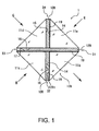
- Fig. 1 is a sectional view showing a constitution of a cross dichroic prism in a first embodiment of the invention.
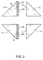
- Fig. 2 is a sectional view showing a first film forming step in a manufacturing process for the cross dichroic prism shown in Fig. 1.
- Fig. 3 is a sectional view showing a first joining step for manufacturing of two prism pairs in the manufacturing process for the cross dichroic prism shown in Fig. 1.
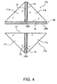
- Fig. 4 is a sectional view showing a third film forming step of forming dichroic films on hypotenuse surfaces of the prism pairs in the manufacturing process for the cross dichroic prism shown in Fig. 1.
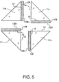
- Fig. 5 is a sectional view showing first and second film forming steps in a manufacturing process for a cross dichroic prism in a second embodiment of the invention.
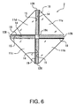
- Fig. 6 is a sectional view showing a structure of the cross dichroic prism in the second embodiment manufactured after the step shown in Fig. 5.
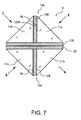
- Fig. 7 is a sectional view showing a structure of a cross dichroic prism in a third embodiment of the invention.
- Fig. 8 is a sectional view showing a structure of a cross dichroic prism in a fourth embodiment of the invention.
- Fig. 9 is a sectional view showing a structure of a cross dichroic prism in a fifth embodiment of the invention.
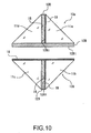
- Fig. 10 is a sectional view showing a manufacturing process for a cross dichroic prism in a sixth embodiment of the invention.
- Fig. 11 is a sectional view showing a structure of the cross dichroic prism in the sixth embodiment of the invention.
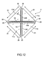
- Fig. 12 is a sectional view showing a state in which gaps are formed at both ends of junctions in a manufacturing step for a cross dichroic prism in a seventh embodiment of the invention.
- Fig. 13 is a sectional view showing a structure of the cross dichroic prism in the seventh embodiment of the invention.
- Fig. 14 is a sectional view showing a manufacturing step for a cross dichroic prism in an eighth embodiment of the invention and is a perspective view showing a state in which reinforcing plates are stuck to both upper and lower ends of the cross dichroic prism.
- Fig. 15 is a perspective view showing a structure of the cross dichroic prism in the eighth embodiment of the invention.
- Fig. 16 is an optical path diagram showing a state in which an image of red R, an image of blue B, and an image of green G are combined using the cross dichroic prism in the first embodiment of the invention shown in Fig. 1.
- Fig. 17 is an optical path diagram showing a state in which an image of red R, an image of blue B, and an image of green G are combined using the cross dichroic prism in the third embodiment of the invention shown in Fig. 7.
- Fig. 18 is an optical path diagram showing a state in which an image of red R, an image of blue B, and an image of green G are combined using a cross dichroic prism in a comparative example 1 shown in Fig. 22.
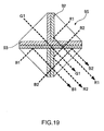
- Fig. 19 is an optical path diagram showing a state in which an image of red R, an image of blue B, and an image of green G are combined using a cross dichroic prism in a comparative example 2 shown in Fig. 23.
- Fig. 20 is a table in which the numbers of times respective rays traverse an adhesive layer in Figs. 16 to 19 are put in order.
- Fig. 21A is a table showing an example of a constitution of a dichroic film that reflects a color red.
- Fig. 21B is a table showing an example of a constitution of a dichroic film that reflects a color blue.
- Fig. 22 is a sectional view showing a constitution of a cross dichroic prism in a comparative example 1.
- Fig. 23 is a sectional view showing a constitution of a cross dichroic prism in a comparative example 2.
- An optical product according to an embodiment of the invention is an optical product including two or more optical elements that have optical planes of glass to be joined to each other.
- a multilayer film, an uppermost layer of which is a silicon oxide film, is formed on an optical plane of a first optical element.
- An optical plane joinable to the optical plane, on which the multilayer film is formed, is formed on a second optical element.
- the optical plane of the first optical element, on which the multilayer film is formed, and the optical plane of the second optical element are joined according to an optical contact method.
- Examples of a specific optical product include a cross dichroic prism.
- the cross dichroic prism is an optical product formed by putting together vertexes forming right angles of a first prism element, a second prism element, a third prism element, and a fourth prism element made of glass that have a shape of a right isosceles triangle right prism and joining respective optical sides adjacent to one another among optical sides orthogonal to one another via dichroic films made of multilayer films.
- the cross dichroic prism is used for trichromatic color separation for white light and trichromatic color combination for projected light.
- the four prism elements have a relation in which the second prism element and the fourth prism elements are provided on both sides of the first prism element and the third prism element is opposed to the first prism element.
- an uppermost layer of the dichroic film in any one of the first to the fourth junctions is made of a silicon oxide layer.
- the silicon oxide layer of the uppermost layer of the dichroic film and the optical side are joined according to an optical contact method.
- a constitution of a cross dichroic prism according to a first embodiment of the invention is shown in Fig. 1 using a section thereof.
- a cross dichroic prism (hereinafter, "dichroic prism") 1 is an optical product (an optical component) formed in substantially a regular square shape in section.
- vertexes forming right angles of four prism elements namely, a first prism element 11a, a second prism element 11b, a third prism elements 11c, and a fourth prism element 11d made of glass that have a shape of a right isosceles triangle right prism are put together to join respective optical sides adjacent to one another among optical sides orthogonal to one another via dichroic films 12R and 12B made of multilayer films.
- the first prism element 11a and the fourth prism element 11d are joined in a fourth junction 34 between the prism elements via the dichroic film 12R according to the optical contact method.
- the second prism element 11b and the third prism element 11c are joined in a second junction 32 between the prism elements via the dichroic film 12R according to the optical contact method.
- the dichroic film 12B is continuously provided over a first junction 31 between the first prism element 11a and the second prism element 11b and a third junction 33 between the third prism element 11c and the fourth prism element 11d.
- the first junction 31 and the third junction 33 are joined to each other via the dichroic film 12B according to the optical contact method.
- all the junctions 31 to 34 are joined according to the optical contact method.
- junctions joined according to the optical contact method are indicated by bold lines as junction surfaces (sections) 19 in order to facilitate explanations. This does not mean that the junction sections 19 by the optical contact method indicated by the bold lines have thickness. The same applies in the drawings referred to below.
- the dichroic films 12R are semi-transparent films that efficiently reflect red light, for example, light with a wavelength of 850nm.
- the dichroic film 12B is a semi-transparent film that efficiently reflects blue light, for example, light with a wavelength of 525nm. Therefore, in the dichroic prism 1, red light R is reflected by the dichroic films 12R to change a direction. Blue light B is reflected by the dichroic film 12B to change a direction. Green light G is transmitted through the dichroic films 12R and 12B. According to such an action, the dichroic prism 1 can combine images of the respective colors and divide white light into rays of the respective colors. Thus, the dichroic prism 1 is one of important optical components in various optical apparatuses such as a projector.
- a manufacturing process for the dichroic prism 1 is schematically shown in Figs. 2 to 4.
- the first prism element 11a to the fourth prism element 11d for example, borosilicate crown optical glass (a refractive index of a d line thereof is 1.51633) called BK7 is used.
- the first prism element 11a to the fourth prism element 11d have a shape of a right prism that is formed by moving a surface of a right isosceles triangle having one apical angle of 90 degrees and the remaining two apical angles of 45 degrees in the vertical direction.
- the dichroic film 12R or 12B is formed on one of two optical sides orthogonal to each other that form each of the apical angles assuming right angles of the first prism element 11a to the fourth prism element 11d.
- the first prism element 11a to the fourth prism element 11d are used in the same manner in other embodiments described later.
- the dichroic film 12R made of a multilayer film is formed as a first multilayer film on a first optical side 15 facing the first prism element 11a among the optical sides of the fourth prism element 11d according to the evaporation method (the first film forming step).
- the dichroic film 12R may be provided on an optical side 14 facing the fourth prism element 11d of the first prism element 11a.
- the dichroic film 12R made of a multilayer film is formed on the-first optical side 15 facing the second prism element 11b among the optical sides of the third prism element 11c according to the evaporation method (the second film forming step).
- the dichroic film 12R is designed to efficiently reflect light with a wavelength of 850nm and designed to have a high reflectance for red light and a high transmittance for blue light and green light.
- the dichroic film 12R in this example is a thin film with thickness of about several tens micrometers formed by stacking a thin film of tantalum pentoxide (Ta 2 O 5 ) and a thin film of silicon oxide (SiO 2 ) by twenty-eight layers in total.
- An uppermost layer 12Rt of the dichroic film 12R is formed as a silicon oxide layer.
- Such a multilayer film is also called a dielectric multilayer film. It is possible to form the multilayer film using the vacuum evaporation method, the ion assist evaporation method, the ion plating method, the sputtering method, and the like. It is possible to form a thin film, which reflects or transmits a desired wavelength, by alternately stacking a layer with a high refractive index and a layer with a low refractive index made of an appropriate material at appropriate thicknesses. As a material of the layer with a high refractive index, it is possible to use titanium oxide (TiO 2 ), niobium pentoxide (Nb 2 O 5 ), and the like other than tantalum oxide. As a material of the layer with a low refractive index, it is possible to use magnesium fluoride (MgF 2 ) and the like other than silicon oxide. In this embodiment, a thin film using silicon oxide is formed at least on an uppermost layer.
- the optical side 15 of the fourth prism element 11d on which the dichroic film 12R is formed and the optical side 14 of the first prism element 11a opposed to the optical side 15 are joined according to the optical contact method (the first joining step).
- the optical side 15 of the third prism element 11c on which the dichroic film 12R is formed and the optical side 14 of the second prism element 11b opposed to the optical side 15 are joined according to the optical contact method (the second joining step).
- a first prism pair 13a of a right isosceles triangle right prism shape in which the first prism element 11a and the fourth prism element 11d are joined and a second prism pair 13b of a right isosceles triangle right prism shape in which the second prism element 11b and the third prism element 11c are joined are formed.
- the optical contact method is publicly known as a method of directly joining glass faces each other.
- the optical contact method is applicable in joining glass faces to each other with a multilayer film put between the glass faces rather than directly joining the glass faces. Therefore, first of all, the uppermost layer 12Rt of the multilayer film formed on the optical side 15 is formed as a silicon oxide film having the same principal components as glass such that coincidence of materials of substantial junctions of the glass optical side 14 opposed to the optical side 15 and the surface 12Rt of the dichroic film 12R is realized.
- the optical side 15 of the fourth prism element 11d exactly has a surface shape of the uppermost layer 12Rt of the dichroic film 12R. It is also possible to secure accuracy of coincidence of surfaces necessary for joining optical surfaces according to the optical contact method by designing a shape of the optical side 15 of the fourth prism element 11d to coincide with a shape of the optical side 14 of the prism element 11a that is opposed to the optical side 15 for joining.
- optical sides 15 and 14 orthogonal to each other which are junction surfaces of the first prism element 11a to the fourth prism element 11d
- the optical sides have a sufficient degree of flatness, for example, surface roughness Ra equal to or lower than 0.5nm and a degree of flatness (a PV value) equal to or lower than 0.5 ⁇ m according to optical grinding (highly accurate grinding).
- a PV value degree of flatness
- both the surfaces are attracted in vacuum because both the surfaces are highly flat surfaces.
- Joining strength is improved by heating the surfaces at 250°C for one hour.
- a heating temperature is desirably 200 to 500°C and more desirably 200 to 300°C.
- two prism pairs namely, the first prism pair 13a and the second prism pair 13b are manufactured.
- Optical hypotenuse surfaces 16 and 17 opposed to vertexes forming right angles of the first prism pair 13a and the second prism pair 13b are optically ground to be highly accurate planes in the same state as above (the surface leveling step).
- the dichroic film 12B made of a multilayer film is formed as a second multilayer film according to the evaporation method on the optical hypotenuse surface 16 opposed to the right angles of the prism pair 13a that is one of the first prism pair 13a and the second prism pair 13b (the third film forming step).
- the dichroic film 12B is formed as a continuous dichroic film continuous over optical sides of the first prism element 11a and the fourth prism element 11d and an end face of the dichroic film 12R.
- the dichroic film 12B is designed to efficiently reflect light with a wavelength of 525nm and designed to have a high reflectivity for blue light and a high transmittance for red light and green light.
- the dichroic film 12B in this example is a thin film having thickness of about several tens micrometers that is formed by stacking a thin film of tantalum pentoxide (Ta 2 O 5 ) and a thin film of silicon oxide (SiO 2 ) by twenty-five layers in total.
- An uppermost layer 12Bt of the dichroic film 12B is formed as a silicon oxide layer.
- the dichroic prism 1 shown in Fig. 1 is manufactured as an optical product by joining the optical hypotenuse surface 16 of the first prism pair 13a and the optical hypotenuse surface 17 of the second prism pair 13b according to the optical contact method (the third joining step).
- the cross dichroic prism 1 in this embodiment can completely eliminate an influence of a layer of an adhesive on an optical path. Therefore, in manufacturing a cross dichroic prism, performance deterioration of which is found in the past because of thickness or an optical characteristic of a layer of an adhesive, the manufacturing method in this embodiment is suitable.
- Figs. 5 and 6 Another embodiment of the invention is shown in Figs. 5 and 6.
- the dichroic film 12R or 12B is formed on each of the optical sides 15 of the first prism elements 11a to the fourth prism element 11d (the first and second film forming steps). Thereafter, the optical sides 15 are joined to the optical sides 14 of the triangular prisms 11a to 11d opposed to the optical sides 15 (the first to third joining steps) to manufacture the dichroic prism 2. Since the steps of film formation and the steps of joining are the same as those in the first embodiment, explanations of the steps are omitted.
- an area along a center axis 19c of the dichroic prism 2 is formed as an area in which it is possible to select presence of the dichroic films 12R and 12B according to a film forming method for the dichroic films 12R and 12B, that is, select whether both the dichroic films should be present, one of the dichroic films should be present, or no dichroic film should be present and the area should be in a hollow state. It is likely that the area is a section that is structurally and optically indefinite. In this regard, the dichroic prism 1 described in the first embodiment is more stable in terms of a structure and optical performance and is preferable.
- Fig. 7 Still another embodiment of the invention is shown in Fig. 7.
- the first prism element 11a to the fourth prism element 11d are used and the prism pairs 13a and 13b are manufactured according to the first film forming step and the first and the second joining steps shown in Figs. 2 and 3.
- the dichroic film 12B is formed on the optical hypotenuse surface 16 of the prism pair 13a and bonded to the optical hypotenuse surface 17 of the other prism pair 13b by an adhesive 20 optically having refractive power substantially equal to that of the prisms 11a to 11d.
- a surface of the dichroic film 12B is formed inside the dichroic prism 3 via a layer of the adhesive 20.
- the layer of the adhesive 20 As in the dichroic prism 1 or 2 in each of the embodiments described above.
- the dichroic film 12B is joined via the adhesive 20, an uppermost layer thereof does not need to be a silicon oxide layer.
- an optical adhesive that is hardened by UV light or visible light is desirable. It is possible to harden the adhesive by shedding light on the adhesive via the first prism element 11a to the fourth prism element 11d.
- a heat-hardening adhesive that is hardened by being heated to temperature of a degree not affecting the sections 19, which are joined according to the optical contact method, may be used.
- an optical adhesive UT20 provided by Kabushiki Kaisha Ades is used as the adhesive.
- a joining jig is prepared to bring triangular prisms into contact with each other via this optical adhesive. Thereafter, a high-pressure mercury-vapor lamp (80W/cm 2 ) is irradiated on the optical adhesive for ten minutes.
- a refractive index (d line) before hardening of the adhesive UT20 is 1.48 and a refractive index (d line) after hardening thereof is 1.52.
- the adhesive UT20 has a refractive index substantially close to BK7 adopted in the prisms.
- Fig. 8 Still another embodiment of the invention is shown in Fig. 8.
- the first prism element 11a to the fourth prism element 11d are used, the first prism pair 13a is manufactured by joining the first prism element 11a and the fourth prism element 11d via the adhesive layer 20 same as that in the third embodiment (the first joining step), and, similarly, the second prism pair 13b is manufactured by joining the second prism element 11b and the third prism element 11c via the adhesive layer 20 (the second joining step).
- Respective optical hypotenuse surfaces opposed to vertexes forming right angles of the first prism pair 13a and the second prism pair 13b are optically ground (the surface leveling step).
- the dichroic film 12B which is made of a multilayer film and has silicon oxide layers in a first layer and an uppermost layer thereof, is formed as a second multilayer film according to the evaporation method on the optical hypotenuse surface opposed to the right angles of the prism pair 13a that is one of the first prism pair 13a and the second prism pair 13b (the third film forming step).
- the dichroic film 12B is a continuous dichroic film formed over optical sides of the two prism elements 11a and 11d.
- the respective optical hypotenuse surfaces of the first prism pair 13a and the second prism pair 13b are joined according to the optical contact method (the third joining step). This makes it possible to manufacture the cross dichroic prism 4 shown in Fig. 8.
- a cross dichroic prism 5 in this embodiment the first prism element 11a to the fourth prism element 11d are used, the first prism pair 13a is manufactured by joining the first prism element 11a and the fourth prism element 11d according to the optical contact method by means of the dichroic film 12R (the first joining step), and the second prism pair 13b is manufactured by joining the second prism element 11b and the third prism element 11c via the adhesive layer 20 (the second joining step).
- Respective optical hypotenuse surfaces opposed to vertexes forming right angles of the first prism pair 13a and the second prism pair 13b are optically ground (the surface leveling step).
- the dichroic film 12B which is made of a multilayer film and has silicon oxide layers in a first layer and an uppermost layer, is formed as a second multilayer film according to the evaporation method on the optical hypotenuse surface opposed to the right angles of the prism pair 13a that is one of the first prism pair 13a and the second prism pair 13b (the third film forming step).
- the dichroic film 12B is a continuous dichroic film formed over optical sides of the two prism elements.
- the respective optical hypotenuse surfaces of the first prism pair 13a and the second prism pair 13b are joined according to the optical contact method (the third joining step). This makes it possible to manufacture the cross dichroic prism 5 shown in Fig. 9.
- two prism pairs are manufactured by joining one prism pair according to the optical contact method and joining the other prism pair using an adhesive.
- a cross dichroic prism 1a in this embodiment is an example in which all junctions are joined according to the optical contact method to eliminate an influence of an adhesive layer.
- the cross dichroic prism 1a is different from that in the first embodiment in that, as shown in Fig. 10, in joining prism pairs, one layer of a silicon oxide layer 18 is provided on an optical hypotenuse surface of the second prism pair 13b on a side where the dichroic film 12B is not formed and, as shown in Fig. 11, the silicon oxide layer 18 and the silicon oxide layer 12Bt of the uppermost layer of the dichroic film 12B are joined according to optical contact method by means of contact between the silicon oxide layers. It is possible to form the silicon oxide layer 18 according to, for example, the evaporation method. It is preferable that thickness of the silicon oxide layer 18 is set in a range of 100 to 10000 angstroms.
- an end face of the dichroic film 12R provided in the second prism pair 13b it is possible to fill an end face of the dichroic film 12R provided in the second prism pair 13b to eliminate gaps by providing the silicon oxide layer 18 on the optical hypotenuse surface of the second prism pair 13b.
- An end face of the dichroic film 12R provided in the first prism pair 13a is filled by the dichroic film 12B and an inner side end face of the dichroic film 12R is integrated with the dichroic film 12B to reduce an optical influence due to the end faces.
- Figs. 12 and 13 Still another embodiment of the invention is shown in Figs. 12 and 13.
- the first prism element 11a to the fourth prism element 11d are formed such that gaps 23 are formed at corner portions 22 on the outside of optically effective areas 21 of the junctions 14 to 17 of the prism elements when the prism elements are stuck together.
- an optically effective area for example, edges or corner portions of an optical product such as a prism manufactured by combining optical elements are not used as optical paths in many cases. Therefore, when the junctions 14 to 17 are joined according to the optical contact method, the corner portions 22 of the dichroic prism 7 are not in optical contact. Thereafter, as shown in Fig. 13, the gaps 23 are sealed by filling the adhesive 20 in the gaps 23.
- the optical adhesive UT20 is used as the adhesive 20 as in the embodiments described above. However, since it is attempted to bond the portions out of the optically effective areas 21, the portions do not need to be optically equivalent to the prisms 11a to lid. For example, it is possible to use an adhesive that is opaque but has high bonding strength. It is possible to perform injection of the adhesive into the gaps 23 in the first joining step or the second joining step.
- the corner portions 22 of the dichroic prism 7 are portions covered by a frame or the like that supports a dichroic prism in an applied apparatus such as a projector and are not used as the optically effective areas 21. Therefore, the portions 22 are bonded by the adhesive 20 and the portions corresponding to the optically effective areas 21 are joined according to the optical contact method. This makes it possible to add an effect of the adhesive 20 without deteriorating optical performance of the dichroic prism 7.
- Adhering strength of surfaces joined according to the optical contact method is generally regarded as extremely strong. Adhering strength of the dichroic films 12R and 12B formed by evaporation is also high. Therefore, durability of the dichroic films 12R and 12B are considered to be sufficiently high against the dichroic prisms 1 and 2 described in the first or the second embodiment.
- the corner portions 22 are put in a support frame or stress concentration is mechanically applied to the corner portions 22. Since the corner portions 22 in the junctions are portions exposed to the outdoor air, the corner portions 22 are most susceptible to intrusion of moisture and a change in the outdoor air temperature. Therefore, the corner portions 22 out of the optically effective areas 21 are portions most easily peeled off. Therefore, it is possible to secure, using the joining method with high reliability adopted in the past, joining properties of the surfaces 14 to 17 joined according to the optical contact method by arranging the adhesive 20 in the portions 22 at the corners of the surfaces 14 to 17 joined according to the optical contact method. It is not usually conceivable that surfaces joined according to the optical contact method are peeled off from the centers or the inside of the surfaces.
- UV curing adhesive it is desirable to use an ultraviolet (UV) curing adhesive as the adhesive. Since edges or corner portions of an optical product that can be manufactured by combining optical elements are exposed on an outer surface of the optical product, even in the case of optical elements that do not transmit an ultraviolet ray, it is possible to join the optical elements using the UV curing adhesive that makes joining work easy. It is possible to use, without hindrance, a UV curing adhesive matching a refractive index of optical elements like the one currently available in the market if the optical elements transmit an ultraviolet ray.
- FIGs. 14 and 15 Still another embodiment of the invention is shown in Figs. 14 and 15.
- reinforcing plates 26 and 27 for support are further stuck to upper and lower surfaces 24 and 25 of the dichroic prism 6, which is manufactured from the first prism element 11a to the fourth prism element 11d, by an adhesive. It is possible to reinforce joining of the first prism element 11a to the fourth prism element 11d using the reinforcing plates 26 and 27 that are joined on upper and lower surfaces of the four prism elements 11a to 11d to extend over all of these prism elements. As a result, it is possible to prevent the junctions 14 to 17 from being peeled apart.
- the reinforcing plates 26 and 27 are manufactured from a member same as the member of the first prism element 11a to the fourth prism element 11d, that is, BK7.
- the member in common it is possible to set coefficients of thermal expansion of the reinforcing plates and the prism elements the same. This makes it possible to prevent occurrence of thermal strain. It is also possible to prevent stray light traveling in the directions of the reinforcing plates 26 and 27 from being reflected by the reinforcing plates and emit the light to the outside from the dichroic prism 6.
- upper and lower portions of the dichroic prism 6 are out of the optical effective areas 21 in the same manner as the corner portions 22.
- a material of the reinforcing plates 26 and 27 do not need to be a material optically equivalent to that of the prisms 11a to 11d. It is possible to form the reinforcing plates 26 and 27 using a member that is opaque but has high strength.
- Fig. 16 shows a state in which an image of red R, an image of blue B, and an image of green G are combined using the dichroic prism 1 in the first embodiment of the invention shown in Fig. 1.
- Fig. 17 shows a state in which an image of red R, an image of blue B, and an image of green G are combined using the dichroic prism 3 in the third embodiment of the invention shown in Fig. 7.
- Fig. 18 shows, as a comparative example 1, a state in which an image of red R, an image of blue B, and an image of green G are combined using a dichroic prism 90 shown in Fig. 22.
- Fig. 19 shows, as a comparative example 2, a state in which an image of red R, an image of blue B, and an image of green G are combined using a dichroic prism 95 shown in Fig. 23.
- the dichroic prism 1 not including a layer of an adhesive, all the rays do not traverse the layer of the adhesive. Thus, it is possible to completely eliminate deterioration in an image quality due to the layer of the adhesive.
- the dichroic prism 3 although a part of the rays traverse the layer of the adhesive, it is possible to hold the number of times of traversing to a minimum number of times, that is, one time. Thus, it is possible to minimize deterioration in the images.
- the optical product in the first aspect of the invention is usable as a dichroic prism used for color separation and color combination by a projector.
- the method of manufacturing an optical product according to the second aspect of the invention is usable in a field of manufacturing of a high-performance cross dichroic prism in which an influence of an adhesive layer is eliminated as much as possible.
Landscapes
- Physics & Mathematics (AREA)
- General Physics & Mathematics (AREA)
- Optics & Photonics (AREA)
- Chemical & Material Sciences (AREA)
- Engineering & Computer Science (AREA)
- Ceramic Engineering (AREA)
- Life Sciences & Earth Sciences (AREA)
- Chemical Kinetics & Catalysis (AREA)
- General Chemical & Material Sciences (AREA)
- Geochemistry & Mineralogy (AREA)
- Materials Engineering (AREA)
- Organic Chemistry (AREA)
- Manufacturing & Machinery (AREA)
- Optical Elements Other Than Lenses (AREA)
Applications Claiming Priority (2)
| Application Number | Priority Date | Filing Date | Title |
|---|---|---|---|
| JP2005081175 | 2005-03-22 | ||
| JP2006007142A JP2006301585A (ja) | 2005-03-22 | 2006-01-16 | 光学製品および光学製品の製造方法 |
Publications (1)
| Publication Number | Publication Date |
|---|---|
| EP1705512A1 true EP1705512A1 (fr) | 2006-09-27 |
Family
ID=36481281
Family Applications (1)
| Application Number | Title | Priority Date | Filing Date |
|---|---|---|---|
| EP06005782A Withdrawn EP1705512A1 (fr) | 2005-03-22 | 2006-03-21 | Produit optique et procédé de fabrication de celui-ci |
Country Status (5)
| Country | Link |
|---|---|
| US (1) | US7684120B2 (fr) |
| EP (1) | EP1705512A1 (fr) |
| JP (1) | JP2006301585A (fr) |
| KR (1) | KR100823751B1 (fr) |
| TW (1) | TWI309730B (fr) |
Cited By (2)
| Publication number | Priority date | Publication date | Assignee | Title |
|---|---|---|---|---|
| EP1998195A1 (fr) * | 2007-05-31 | 2008-12-03 | Schott AG | Filtre d'interférence et son procédé de fabrication |
| CN101195518B (zh) * | 2006-11-07 | 2012-03-21 | 柯尼卡美能达精密光学株式会社 | 用于制造光学器件的方法和接合夹具 |
Families Citing this family (15)
| Publication number | Priority date | Publication date | Assignee | Title |
|---|---|---|---|---|
| US20080302039A1 (en) * | 2007-06-08 | 2008-12-11 | Applied Coatings Group, Inc. | Decorative Effect for Glass Bodies |
| US20100330339A1 (en) * | 2007-06-08 | 2010-12-30 | Applied Coatings Group, Inc. | Decorative effect for glass bodies |
| JP2010276941A (ja) * | 2009-05-29 | 2010-12-09 | Fujifilm Corp | 接合型光学素子の製造方法 |
| US8277049B2 (en) * | 2010-02-02 | 2012-10-02 | National Kaohsiung First University Of Science And Technology | Projector using LEDs as light sources |
| KR20120071960A (ko) | 2010-12-23 | 2012-07-03 | 삼성모바일디스플레이주식회사 | 광학 접촉 결합을 이용한 금속 및 글라스 접합 방법, 이를 이용한 표시 장치의 제조 방법, 및 상기 제조 방법에 의해 만들어진 표시 장치 |
| JP2013228530A (ja) * | 2012-04-25 | 2013-11-07 | Seiko Epson Corp | プロジェクター |
| DE102016110351B4 (de) | 2016-06-03 | 2019-08-29 | Carl Zeiss Meditec Ag | Verfahren zur Herstellung eines optischen Elements |
| US11011503B2 (en) | 2017-12-15 | 2021-05-18 | Invensas Bonding Technologies, Inc. | Direct-bonded optoelectronic interconnect for high-density integrated photonics |
| US11256004B2 (en) * | 2018-03-20 | 2022-02-22 | Invensas Bonding Technologies, Inc. | Direct-bonded lamination for improved image clarity in optical devices |
| JP7172188B2 (ja) * | 2018-06-29 | 2022-11-16 | セイコーエプソン株式会社 | 頭部装着型表示装置 |
| JP6965836B2 (ja) * | 2018-07-03 | 2021-11-10 | セイコーエプソン株式会社 | クロスダイクロイックプリズム、画像表示モジュールおよび画像表示装置 |
| JP2021136071A (ja) * | 2020-02-24 | 2021-09-13 | セイコーエプソン株式会社 | 光源装置、照明装置およびプロジェクター |
| US20220107269A1 (en) * | 2020-10-02 | 2022-04-07 | Pall Corporation | Refractometer with single use prism and reusable optical system |
| CN112817073B (zh) * | 2020-12-31 | 2022-02-01 | 南京航空航天大学 | 一种基于无反射滤波器原理的红外吸波器 |
| FR3130404B1 (fr) * | 2021-12-09 | 2025-02-21 | Valeo Comfort & Driving Assistance | Lame partiellement réfléchissante, dispositif d’affichage comprenant une telle lame, planche de bord et dispositif d’affichage tête-haute comprenant un tel dispositif d’affichage |
Citations (6)
| Publication number | Priority date | Publication date | Assignee | Title |
|---|---|---|---|---|
| US3880632A (en) * | 1973-08-30 | 1975-04-29 | Galina Yakovlevna Podvigalkina | Method of joining optical glass parts |
| JPH03149516A (ja) * | 1989-11-06 | 1991-06-26 | Victor Co Of Japan Ltd | ダイクロイックプリズム |
| JPH03149415A (ja) * | 1989-10-12 | 1991-06-26 | Uingu Haisera:Kk | セラミックス製軸受 |
| EP1008567A1 (fr) * | 1997-07-23 | 2000-06-14 | Hamamatsu Photonics K.K. | Procede permettant de coller des elements en verre |
| US6411449B1 (en) * | 1998-04-08 | 2002-06-25 | Seiko Epson Corporation | Light-selective prism, projection display apparatus using the same, and method of manufacturing light-selective prism |
| EP1406110A1 (fr) * | 2002-10-01 | 2004-04-07 | ASML Holding, N.V. | Cube optique diviseur de faisceaux ou polarisant et méthode de fabrication |
Family Cites Families (14)
| Publication number | Priority date | Publication date | Assignee | Title |
|---|---|---|---|---|
| JPH03149416A (ja) | 1989-11-01 | 1991-06-26 | Hitachi Ltd | 軸受固定機構 |
| JP3324197B2 (ja) | 1993-05-18 | 2002-09-17 | セイコーエプソン株式会社 | プリズムおよびこれを用いたプロジェクター |
| JPH095518A (ja) | 1995-06-19 | 1997-01-10 | Nikon Corp | 偏光ビームスプリッター及びその製造方法 |
| JPH0915405A (ja) | 1995-06-28 | 1997-01-17 | Nikon Corp | クロスダイクロイックプリズム及びその製造方法 |
| JPH09309053A (ja) | 1996-05-23 | 1997-12-02 | Sigma Koki Kk | 光学部品の研磨方法及び光学部品 |
| JP3473335B2 (ja) * | 1996-08-19 | 2003-12-02 | セイコーエプソン株式会社 | 投写型表示装置 |
| JP3371784B2 (ja) | 1996-12-06 | 2003-01-27 | セイコーエプソン株式会社 | クロスダイクロイックプリズム、プリズムユニット、および、投写型表示装置 |
| KR100276081B1 (ko) * | 1997-10-24 | 2001-02-01 | 정선종 | 두 파장용 편광 광 분할기 및 그 제작방법 |
| JP2002189109A (ja) | 2000-10-10 | 2002-07-05 | Nikon Corp | クロスダイクロイックプリズムならびにその製造方法 |
| JP2003075614A (ja) | 2001-09-03 | 2003-03-12 | Hitachi Ltd | プリズム、プリズムの製造方法、光学ユニット及び投射型表示装置 |
| JP2003294937A (ja) | 2002-03-29 | 2003-10-15 | Sumitomo Osaka Cement Co Ltd | 光共振器および波長管理モジュール |
| JP2004163714A (ja) | 2002-11-14 | 2004-06-10 | Fuji Photo Optical Co Ltd | クロスダイクロイックプリズムおよびこれを用いた反射型液晶プロジェクタ装置 |
| JP2004279495A (ja) | 2003-03-13 | 2004-10-07 | Nikon Corp | ビームスプリッタおよび光学測定機 |
| US7379247B2 (en) * | 2005-05-23 | 2008-05-27 | Olympus Imaging Corp. | Image pickup apparatus |
-
2006
- 2006-01-16 JP JP2006007142A patent/JP2006301585A/ja active Pending
- 2006-03-09 TW TW095107953A patent/TWI309730B/zh not_active IP Right Cessation
- 2006-03-20 US US11/378,415 patent/US7684120B2/en not_active Expired - Fee Related
- 2006-03-21 KR KR1020060025639A patent/KR100823751B1/ko not_active Expired - Fee Related
- 2006-03-21 EP EP06005782A patent/EP1705512A1/fr not_active Withdrawn
Patent Citations (6)
| Publication number | Priority date | Publication date | Assignee | Title |
|---|---|---|---|---|
| US3880632A (en) * | 1973-08-30 | 1975-04-29 | Galina Yakovlevna Podvigalkina | Method of joining optical glass parts |
| JPH03149415A (ja) * | 1989-10-12 | 1991-06-26 | Uingu Haisera:Kk | セラミックス製軸受 |
| JPH03149516A (ja) * | 1989-11-06 | 1991-06-26 | Victor Co Of Japan Ltd | ダイクロイックプリズム |
| EP1008567A1 (fr) * | 1997-07-23 | 2000-06-14 | Hamamatsu Photonics K.K. | Procede permettant de coller des elements en verre |
| US6411449B1 (en) * | 1998-04-08 | 2002-06-25 | Seiko Epson Corporation | Light-selective prism, projection display apparatus using the same, and method of manufacturing light-selective prism |
| EP1406110A1 (fr) * | 2002-10-01 | 2004-04-07 | ASML Holding, N.V. | Cube optique diviseur de faisceaux ou polarisant et méthode de fabrication |
Non-Patent Citations (2)
| Title |
|---|
| PATENT ABSTRACTS OF JAPAN vol. 015, no. 374 (M - 1160) 20 September 1991 (1991-09-20) * |
| PATENT ABSTRACTS OF JAPAN vol. 015, no. 380 (P - 1256) 25 September 1991 (1991-09-25) * |
Cited By (4)
| Publication number | Priority date | Publication date | Assignee | Title |
|---|---|---|---|---|
| CN101195518B (zh) * | 2006-11-07 | 2012-03-21 | 柯尼卡美能达精密光学株式会社 | 用于制造光学器件的方法和接合夹具 |
| EP1998195A1 (fr) * | 2007-05-31 | 2008-12-03 | Schott AG | Filtre d'interférence et son procédé de fabrication |
| CN101393294B (zh) * | 2007-05-31 | 2011-06-15 | 肖特股份公司 | 干涉滤光片及其制造方法 |
| US8000002B2 (en) | 2007-05-31 | 2011-08-16 | Schott Ag | Interference filter and method for producing it |
Also Published As
| Publication number | Publication date |
|---|---|
| KR20060102289A (ko) | 2006-09-27 |
| JP2006301585A (ja) | 2006-11-02 |
| TWI309730B (en) | 2009-05-11 |
| US7684120B2 (en) | 2010-03-23 |
| KR100823751B1 (ko) | 2008-04-21 |
| TW200700772A (en) | 2007-01-01 |
| US20060215123A1 (en) | 2006-09-28 |
Similar Documents
| Publication | Publication Date | Title |
|---|---|---|
| US7684120B2 (en) | Optical product and method of manufacturing the optical product | |
| JP2024055896A (ja) | 光学デバイスにおける改善された写像性のための直接結合積層 | |
| US8842365B2 (en) | Phase difference element and method for manufacturing the same | |
| US20130038933A1 (en) | Beam splitter and method for manufacturing the same | |
| CN109001849B (zh) | 一种宽波长域的高效减反射膜及光学系统 | |
| TWI352825B (fr) | ||
| US20220155510A1 (en) | Optical element and projection image display apparatus | |
| US11269218B2 (en) | Phase difference compensation element, liquid crystal display device and projection type image display device | |
| WO2018105445A1 (fr) | Élément de formation d'image aérienne réflexif | |
| KR20190125189A (ko) | 코팅된 광학 부재, 코팅된 광학 부재를 갖는 부품 및 이의 제조 방법 | |
| JP2020008606A (ja) | クロスダイクロイックプリズム、画像表示モジュールおよび画像表示装置 | |
| CN100406920C (zh) | 光学制品及光学制品的制造方法 | |
| JP2006195301A (ja) | 光学素子 | |
| EP1276000B1 (fr) | Séparateur des polarisations et procédé pour sa fabrication | |
| TW399153B (en) | Optical element and its production method | |
| JP2006071754A (ja) | 偏光ビームスプリッター及びその製造方法 | |
| JP5458545B2 (ja) | 光学物品の製造方法 | |
| JPH05264802A (ja) | 多層反射防止膜 | |
| JPH0985874A (ja) | 光学薄膜およびその製造方法 | |
| CN112105974A (zh) | 相位差补偿元件、液晶显示装置、以及投射型图像显示装置 | |
| JPH07168017A (ja) | 色分解光学フィルタ | |
| JP2007078779A (ja) | クロスダイクロイックプリズム、光学装置、プロジェクタ、および、クロスダイクロイックプリズムの製造方法 | |
| JP2003344654A (ja) | 光学素子および偏光変換素子 | |
| WO2007129375A1 (fr) | Composant de dispositif optique | |
| JPS6114485B2 (fr) |
Legal Events
| Date | Code | Title | Description |
|---|---|---|---|
| PUAI | Public reference made under article 153(3) epc to a published international application that has entered the european phase |
Free format text: ORIGINAL CODE: 0009012 |
|
| AK | Designated contracting states |
Kind code of ref document: A1 Designated state(s): AT BE BG CH CY CZ DE DK EE ES FI FR GB GR HU IE IS IT LI LT LU LV MC NL PL PT RO SE SI SK TR |
|
| AX | Request for extension of the european patent |
Extension state: AL BA HR MK YU |
|
| 17P | Request for examination filed |
Effective date: 20061018 |
|
| AKX | Designation fees paid |
Designated state(s): DE FR GB NL |
|
| STAA | Information on the status of an ep patent application or granted ep patent |
Free format text: STATUS: THE APPLICATION HAS BEEN WITHDRAWN |
|
| 18W | Application withdrawn |
Effective date: 20090123 |