EP1715512A2 - Halbleitervorrichtung und ein Verfahren dessen Herstellung - Google Patents
Halbleitervorrichtung und ein Verfahren dessen Herstellung Download PDFInfo
- Publication number
- EP1715512A2 EP1715512A2 EP06116868A EP06116868A EP1715512A2 EP 1715512 A2 EP1715512 A2 EP 1715512A2 EP 06116868 A EP06116868 A EP 06116868A EP 06116868 A EP06116868 A EP 06116868A EP 1715512 A2 EP1715512 A2 EP 1715512A2
- Authority
- EP
- European Patent Office
- Prior art keywords
- semiconductor device
- semiconductor chip
- board
- chip
- connection
- Prior art date
- Legal status (The legal status is an assumption and is not a legal conclusion. Google has not performed a legal analysis and makes no representation as to the accuracy of the status listed.)
- Withdrawn
Links
Images










Classifications
-
- H—ELECTRICITY
- H05—ELECTRIC TECHNIQUES NOT OTHERWISE PROVIDED FOR
- H05K—PRINTED CIRCUITS; CASINGS OR CONSTRUCTIONAL DETAILS OF ELECTRIC APPARATUS; MANUFACTURE OF ASSEMBLAGES OF ELECTRICAL COMPONENTS
- H05K3/00—Apparatus or processes for manufacturing printed circuits
- H05K3/46—Manufacturing multilayer circuits
- H05K3/4602—Manufacturing multilayer circuits characterized by a special circuit board as base or central core whereon additional circuit layers are built or additional circuit boards are laminated
-
- H—ELECTRICITY
- H10—SEMICONDUCTOR DEVICES; ELECTRIC SOLID-STATE DEVICES NOT OTHERWISE PROVIDED FOR
- H10W—GENERIC PACKAGES, INTERCONNECTIONS, CONNECTORS OR OTHER CONSTRUCTIONAL DETAILS OF DEVICES COVERED BY CLASS H10
- H10W76/00—Containers; Fillings or auxiliary members therefor; Seals
- H10W76/10—Containers or parts thereof
- H10W76/12—Containers or parts thereof characterised by their shape
-
- H—ELECTRICITY
- H10—SEMICONDUCTOR DEVICES; ELECTRIC SOLID-STATE DEVICES NOT OTHERWISE PROVIDED FOR
- H10W—GENERIC PACKAGES, INTERCONNECTIONS, CONNECTORS OR OTHER CONSTRUCTIONAL DETAILS OF DEVICES COVERED BY CLASS H10
- H10W42/00—Arrangements for protection of devices
- H10W42/20—Arrangements for protection of devices protecting against electromagnetic or particle radiation, e.g. light, X-rays, gamma-rays or electrons
- H10W42/261—Arrangements for protection of devices protecting against electromagnetic or particle radiation, e.g. light, X-rays, gamma-rays or electrons characterised by their shapes or dispositions
- H10W42/276—Arrangements for protection of devices protecting against electromagnetic or particle radiation, e.g. light, X-rays, gamma-rays or electrons characterised by their shapes or dispositions the arrangements being on an external surface of the package, e.g. on the outer surface of an encapsulation
-
- H—ELECTRICITY
- H10—SEMICONDUCTOR DEVICES; ELECTRIC SOLID-STATE DEVICES NOT OTHERWISE PROVIDED FOR
- H10W—GENERIC PACKAGES, INTERCONNECTIONS, CONNECTORS OR OTHER CONSTRUCTIONAL DETAILS OF DEVICES COVERED BY CLASS H10
- H10W70/00—Package substrates; Interposers; Redistribution layers [RDL]
- H10W70/01—Manufacture or treatment
- H10W70/05—Manufacture or treatment of insulating or insulated package substrates, or of interposers, or of redistribution layers
- H10W70/095—Manufacture or treatment of insulating or insulated package substrates, or of interposers, or of redistribution layers of vias therein
-
- H—ELECTRICITY
- H10—SEMICONDUCTOR DEVICES; ELECTRIC SOLID-STATE DEVICES NOT OTHERWISE PROVIDED FOR
- H10W—GENERIC PACKAGES, INTERCONNECTIONS, CONNECTORS OR OTHER CONSTRUCTIONAL DETAILS OF DEVICES COVERED BY CLASS H10
- H10W70/00—Package substrates; Interposers; Redistribution layers [RDL]
- H10W70/60—Insulating or insulated package substrates; Interposers; Redistribution layers
- H10W70/62—Insulating or insulated package substrates; Interposers; Redistribution layers characterised by their interconnections
- H10W70/63—Vias, e.g. via plugs
- H10W70/635—Through-vias
-
- H—ELECTRICITY
- H10—SEMICONDUCTOR DEVICES; ELECTRIC SOLID-STATE DEVICES NOT OTHERWISE PROVIDED FOR
- H10W—GENERIC PACKAGES, INTERCONNECTIONS, CONNECTORS OR OTHER CONSTRUCTIONAL DETAILS OF DEVICES COVERED BY CLASS H10
- H10W70/00—Package substrates; Interposers; Redistribution layers [RDL]
- H10W70/60—Insulating or insulated package substrates; Interposers; Redistribution layers
- H10W70/62—Insulating or insulated package substrates; Interposers; Redistribution layers characterised by their interconnections
- H10W70/65—Shapes or dispositions of interconnections
-
- H—ELECTRICITY
- H10—SEMICONDUCTOR DEVICES; ELECTRIC SOLID-STATE DEVICES NOT OTHERWISE PROVIDED FOR
- H10W—GENERIC PACKAGES, INTERCONNECTIONS, CONNECTORS OR OTHER CONSTRUCTIONAL DETAILS OF DEVICES COVERED BY CLASS H10
- H10W70/00—Package substrates; Interposers; Redistribution layers [RDL]
- H10W70/60—Insulating or insulated package substrates; Interposers; Redistribution layers
- H10W70/67—Insulating or insulated package substrates; Interposers; Redistribution layers characterised by their insulating layers or insulating parts
- H10W70/68—Shapes or dispositions thereof
- H10W70/6875—Shapes or dispositions thereof being on a metallic substrate, e.g. insulated metal substrates [IMS]
-
- H—ELECTRICITY
- H10—SEMICONDUCTOR DEVICES; ELECTRIC SOLID-STATE DEVICES NOT OTHERWISE PROVIDED FOR
- H10W—GENERIC PACKAGES, INTERCONNECTIONS, CONNECTORS OR OTHER CONSTRUCTIONAL DETAILS OF DEVICES COVERED BY CLASS H10
- H10W74/00—Encapsulations, e.g. protective coatings
- H10W74/10—Encapsulations, e.g. protective coatings characterised by their shape or disposition
- H10W74/111—Encapsulations, e.g. protective coatings characterised by their shape or disposition the semiconductor body being completely enclosed
- H10W74/114—Encapsulations, e.g. protective coatings characterised by their shape or disposition the semiconductor body being completely enclosed by a substrate and the encapsulations
-
- H—ELECTRICITY
- H10—SEMICONDUCTOR DEVICES; ELECTRIC SOLID-STATE DEVICES NOT OTHERWISE PROVIDED FOR
- H10W—GENERIC PACKAGES, INTERCONNECTIONS, CONNECTORS OR OTHER CONSTRUCTIONAL DETAILS OF DEVICES COVERED BY CLASS H10
- H10W74/00—Encapsulations, e.g. protective coatings
- H10W74/10—Encapsulations, e.g. protective coatings characterised by their shape or disposition
- H10W74/111—Encapsulations, e.g. protective coatings characterised by their shape or disposition the semiconductor body being completely enclosed
- H10W74/114—Encapsulations, e.g. protective coatings characterised by their shape or disposition the semiconductor body being completely enclosed by a substrate and the encapsulations
- H10W74/117—Encapsulations, e.g. protective coatings characterised by their shape or disposition the semiconductor body being completely enclosed by a substrate and the encapsulations the substrate having spherical bumps for external connection
-
- H—ELECTRICITY
- H10—SEMICONDUCTOR DEVICES; ELECTRIC SOLID-STATE DEVICES NOT OTHERWISE PROVIDED FOR
- H10W—GENERIC PACKAGES, INTERCONNECTIONS, CONNECTORS OR OTHER CONSTRUCTIONAL DETAILS OF DEVICES COVERED BY CLASS H10
- H10W74/00—Encapsulations, e.g. protective coatings
- H10W74/10—Encapsulations, e.g. protective coatings characterised by their shape or disposition
- H10W74/111—Encapsulations, e.g. protective coatings characterised by their shape or disposition the semiconductor body being completely enclosed
- H10W74/121—Encapsulations, e.g. protective coatings characterised by their shape or disposition the semiconductor body being completely enclosed by multiple encapsulations, e.g. by a thin protective coating and a thick encapsulation
-
- H—ELECTRICITY
- H10—SEMICONDUCTOR DEVICES; ELECTRIC SOLID-STATE DEVICES NOT OTHERWISE PROVIDED FOR
- H10W—GENERIC PACKAGES, INTERCONNECTIONS, CONNECTORS OR OTHER CONSTRUCTIONAL DETAILS OF DEVICES COVERED BY CLASS H10
- H10W76/00—Containers; Fillings or auxiliary members therefor; Seals
- H10W76/40—Fillings or auxiliary members in containers, e.g. centering rings
- H10W76/42—Fillings
- H10W76/47—Solid or gel fillings
-
- H—ELECTRICITY
- H10—SEMICONDUCTOR DEVICES; ELECTRIC SOLID-STATE DEVICES NOT OTHERWISE PROVIDED FOR
- H10W—GENERIC PACKAGES, INTERCONNECTIONS, CONNECTORS OR OTHER CONSTRUCTIONAL DETAILS OF DEVICES COVERED BY CLASS H10
- H10W76/00—Containers; Fillings or auxiliary members therefor; Seals
- H10W76/60—Seals
-
- H—ELECTRICITY
- H10—SEMICONDUCTOR DEVICES; ELECTRIC SOLID-STATE DEVICES NOT OTHERWISE PROVIDED FOR
- H10W—GENERIC PACKAGES, INTERCONNECTIONS, CONNECTORS OR OTHER CONSTRUCTIONAL DETAILS OF DEVICES COVERED BY CLASS H10
- H10W90/00—Package configurations
-
- H—ELECTRICITY
- H10—SEMICONDUCTOR DEVICES; ELECTRIC SOLID-STATE DEVICES NOT OTHERWISE PROVIDED FOR
- H10W—GENERIC PACKAGES, INTERCONNECTIONS, CONNECTORS OR OTHER CONSTRUCTIONAL DETAILS OF DEVICES COVERED BY CLASS H10
- H10W90/00—Package configurations
- H10W90/401—Package configurations characterised by multiple insulating or insulated package substrates, interposers or RDLs
-
- H—ELECTRICITY
- H10—SEMICONDUCTOR DEVICES; ELECTRIC SOLID-STATE DEVICES NOT OTHERWISE PROVIDED FOR
- H10W—GENERIC PACKAGES, INTERCONNECTIONS, CONNECTORS OR OTHER CONSTRUCTIONAL DETAILS OF DEVICES COVERED BY CLASS H10
- H10W90/00—Package configurations
- H10W90/701—Package configurations characterised by the relative positions of pads or connectors relative to package parts
-
- H—ELECTRICITY
- H05—ELECTRIC TECHNIQUES NOT OTHERWISE PROVIDED FOR
- H05K—PRINTED CIRCUITS; CASINGS OR CONSTRUCTIONAL DETAILS OF ELECTRIC APPARATUS; MANUFACTURE OF ASSEMBLAGES OF ELECTRICAL COMPONENTS
- H05K2201/00—Indexing scheme relating to printed circuits covered by H05K1/00
- H05K2201/09—Shape and layout
- H05K2201/09209—Shape and layout details of conductors
- H05K2201/095—Conductive through-holes or vias
- H05K2201/0959—Plated through-holes or plated blind vias filled with insulating material
-
- H—ELECTRICITY
- H05—ELECTRIC TECHNIQUES NOT OTHERWISE PROVIDED FOR
- H05K—PRINTED CIRCUITS; CASINGS OR CONSTRUCTIONAL DETAILS OF ELECTRIC APPARATUS; MANUFACTURE OF ASSEMBLAGES OF ELECTRICAL COMPONENTS
- H05K2201/00—Indexing scheme relating to printed circuits covered by H05K1/00
- H05K2201/09—Shape and layout
- H05K2201/09209—Shape and layout details of conductors
- H05K2201/09654—Shape and layout details of conductors covering at least two types of conductors provided for in H05K2201/09218 - H05K2201/095
- H05K2201/09672—Superposed layout, i.e. in different planes
-
- H—ELECTRICITY
- H10—SEMICONDUCTOR DEVICES; ELECTRIC SOLID-STATE DEVICES NOT OTHERWISE PROVIDED FOR
- H10W—GENERIC PACKAGES, INTERCONNECTIONS, CONNECTORS OR OTHER CONSTRUCTIONAL DETAILS OF DEVICES COVERED BY CLASS H10
- H10W70/00—Package substrates; Interposers; Redistribution layers [RDL]
- H10W70/60—Insulating or insulated package substrates; Interposers; Redistribution layers
- H10W70/67—Insulating or insulated package substrates; Interposers; Redistribution layers characterised by their insulating layers or insulating parts
- H10W70/68—Shapes or dispositions thereof
- H10W70/682—Shapes or dispositions thereof comprising holes having chips therein
-
- H—ELECTRICITY
- H10—SEMICONDUCTOR DEVICES; ELECTRIC SOLID-STATE DEVICES NOT OTHERWISE PROVIDED FOR
- H10W—GENERIC PACKAGES, INTERCONNECTIONS, CONNECTORS OR OTHER CONSTRUCTIONAL DETAILS OF DEVICES COVERED BY CLASS H10
- H10W70/00—Package substrates; Interposers; Redistribution layers [RDL]
- H10W70/60—Insulating or insulated package substrates; Interposers; Redistribution layers
- H10W70/67—Insulating or insulated package substrates; Interposers; Redistribution layers characterised by their insulating layers or insulating parts
- H10W70/68—Shapes or dispositions thereof
- H10W70/685—Shapes or dispositions thereof comprising multiple insulating layers
-
- H—ELECTRICITY
- H10—SEMICONDUCTOR DEVICES; ELECTRIC SOLID-STATE DEVICES NOT OTHERWISE PROVIDED FOR
- H10W—GENERIC PACKAGES, INTERCONNECTIONS, CONNECTORS OR OTHER CONSTRUCTIONAL DETAILS OF DEVICES COVERED BY CLASS H10
- H10W72/00—Interconnections or connectors in packages
- H10W72/071—Connecting or disconnecting
- H10W72/072—Connecting or disconnecting of bump connectors
- H10W72/07231—Techniques
- H10W72/07236—Soldering or alloying
-
- H—ELECTRICITY
- H10—SEMICONDUCTOR DEVICES; ELECTRIC SOLID-STATE DEVICES NOT OTHERWISE PROVIDED FOR
- H10W—GENERIC PACKAGES, INTERCONNECTIONS, CONNECTORS OR OTHER CONSTRUCTIONAL DETAILS OF DEVICES COVERED BY CLASS H10
- H10W72/00—Interconnections or connectors in packages
- H10W72/20—Bump connectors, e.g. solder bumps or copper pillars; Dummy bumps; Thermal bumps
- H10W72/251—Materials
- H10W72/252—Materials comprising solid metals or solid metalloids, e.g. PbSn, Ag or Cu
-
- H—ELECTRICITY
- H10—SEMICONDUCTOR DEVICES; ELECTRIC SOLID-STATE DEVICES NOT OTHERWISE PROVIDED FOR
- H10W—GENERIC PACKAGES, INTERCONNECTIONS, CONNECTORS OR OTHER CONSTRUCTIONAL DETAILS OF DEVICES COVERED BY CLASS H10
- H10W72/00—Interconnections or connectors in packages
- H10W72/851—Dispositions of multiple connectors or interconnections
- H10W72/874—On different surfaces
- H10W72/877—Bump connectors and die-attach connectors
-
- H—ELECTRICITY
- H10—SEMICONDUCTOR DEVICES; ELECTRIC SOLID-STATE DEVICES NOT OTHERWISE PROVIDED FOR
- H10W—GENERIC PACKAGES, INTERCONNECTIONS, CONNECTORS OR OTHER CONSTRUCTIONAL DETAILS OF DEVICES COVERED BY CLASS H10
- H10W72/00—Interconnections or connectors in packages
- H10W72/851—Dispositions of multiple connectors or interconnections
- H10W72/874—On different surfaces
- H10W72/884—Die-attach connectors and bond wires
-
- H—ELECTRICITY
- H10—SEMICONDUCTOR DEVICES; ELECTRIC SOLID-STATE DEVICES NOT OTHERWISE PROVIDED FOR
- H10W—GENERIC PACKAGES, INTERCONNECTIONS, CONNECTORS OR OTHER CONSTRUCTIONAL DETAILS OF DEVICES COVERED BY CLASS H10
- H10W74/00—Encapsulations, e.g. protective coatings
- H10W74/10—Encapsulations, e.g. protective coatings characterised by their shape or disposition
- H10W74/15—Encapsulations, e.g. protective coatings characterised by their shape or disposition on active surfaces of flip-chip devices, e.g. underfills
-
- H—ELECTRICITY
- H10—SEMICONDUCTOR DEVICES; ELECTRIC SOLID-STATE DEVICES NOT OTHERWISE PROVIDED FOR
- H10W—GENERIC PACKAGES, INTERCONNECTIONS, CONNECTORS OR OTHER CONSTRUCTIONAL DETAILS OF DEVICES COVERED BY CLASS H10
- H10W90/00—Package configurations
- H10W90/20—Configurations of stacked chips
- H10W90/288—Configurations of stacked chips characterised by arrangements for thermal management of the stacked chips
-
- H—ELECTRICITY
- H10—SEMICONDUCTOR DEVICES; ELECTRIC SOLID-STATE DEVICES NOT OTHERWISE PROVIDED FOR
- H10W—GENERIC PACKAGES, INTERCONNECTIONS, CONNECTORS OR OTHER CONSTRUCTIONAL DETAILS OF DEVICES COVERED BY CLASS H10
- H10W90/00—Package configurations
- H10W90/20—Configurations of stacked chips
- H10W90/291—Configurations of stacked chips characterised by containers, encapsulations, or other housings for the stacked chips
-
- H—ELECTRICITY
- H10—SEMICONDUCTOR DEVICES; ELECTRIC SOLID-STATE DEVICES NOT OTHERWISE PROVIDED FOR
- H10W—GENERIC PACKAGES, INTERCONNECTIONS, CONNECTORS OR OTHER CONSTRUCTIONAL DETAILS OF DEVICES COVERED BY CLASS H10
- H10W90/00—Package configurations
- H10W90/20—Configurations of stacked chips
- H10W90/297—Configurations of stacked chips characterised by the through-semiconductor vias [TSVs] in the stacked chips
-
- H—ELECTRICITY
- H10—SEMICONDUCTOR DEVICES; ELECTRIC SOLID-STATE DEVICES NOT OTHERWISE PROVIDED FOR
- H10W—GENERIC PACKAGES, INTERCONNECTIONS, CONNECTORS OR OTHER CONSTRUCTIONAL DETAILS OF DEVICES COVERED BY CLASS H10
- H10W90/00—Package configurations
- H10W90/701—Package configurations characterised by the relative positions of pads or connectors relative to package parts
- H10W90/721—Package configurations characterised by the relative positions of pads or connectors relative to package parts of bump connectors
- H10W90/722—Package configurations characterised by the relative positions of pads or connectors relative to package parts of bump connectors between stacked chips
-
- H—ELECTRICITY
- H10—SEMICONDUCTOR DEVICES; ELECTRIC SOLID-STATE DEVICES NOT OTHERWISE PROVIDED FOR
- H10W—GENERIC PACKAGES, INTERCONNECTIONS, CONNECTORS OR OTHER CONSTRUCTIONAL DETAILS OF DEVICES COVERED BY CLASS H10
- H10W90/00—Package configurations
- H10W90/701—Package configurations characterised by the relative positions of pads or connectors relative to package parts
- H10W90/721—Package configurations characterised by the relative positions of pads or connectors relative to package parts of bump connectors
- H10W90/724—Package configurations characterised by the relative positions of pads or connectors relative to package parts of bump connectors between a chip and a stacked insulating package substrate, interposer or RDL
-
- H—ELECTRICITY
- H10—SEMICONDUCTOR DEVICES; ELECTRIC SOLID-STATE DEVICES NOT OTHERWISE PROVIDED FOR
- H10W—GENERIC PACKAGES, INTERCONNECTIONS, CONNECTORS OR OTHER CONSTRUCTIONAL DETAILS OF DEVICES COVERED BY CLASS H10
- H10W90/00—Package configurations
- H10W90/701—Package configurations characterised by the relative positions of pads or connectors relative to package parts
- H10W90/731—Package configurations characterised by the relative positions of pads or connectors relative to package parts of die-attach connectors
- H10W90/734—Package configurations characterised by the relative positions of pads or connectors relative to package parts of die-attach connectors between a chip and a stacked insulating package substrate, interposer or RDL
-
- H—ELECTRICITY
- H10—SEMICONDUCTOR DEVICES; ELECTRIC SOLID-STATE DEVICES NOT OTHERWISE PROVIDED FOR
- H10W—GENERIC PACKAGES, INTERCONNECTIONS, CONNECTORS OR OTHER CONSTRUCTIONAL DETAILS OF DEVICES COVERED BY CLASS H10
- H10W90/00—Package configurations
- H10W90/701—Package configurations characterised by the relative positions of pads or connectors relative to package parts
- H10W90/731—Package configurations characterised by the relative positions of pads or connectors relative to package parts of die-attach connectors
- H10W90/736—Package configurations characterised by the relative positions of pads or connectors relative to package parts of die-attach connectors between a chip and a stacked lead frame, conducting package substrate or heat sink
-
- H—ELECTRICITY
- H10—SEMICONDUCTOR DEVICES; ELECTRIC SOLID-STATE DEVICES NOT OTHERWISE PROVIDED FOR
- H10W—GENERIC PACKAGES, INTERCONNECTIONS, CONNECTORS OR OTHER CONSTRUCTIONAL DETAILS OF DEVICES COVERED BY CLASS H10
- H10W90/00—Package configurations
- H10W90/701—Package configurations characterised by the relative positions of pads or connectors relative to package parts
- H10W90/751—Package configurations characterised by the relative positions of pads or connectors relative to package parts of bond wires
- H10W90/754—Package configurations characterised by the relative positions of pads or connectors relative to package parts of bond wires between a chip and a stacked insulating package substrate, interposer or RDL
Definitions
- the present invention generally relates to semiconductor devices, and more particularly relates to a semiconductor device of the ball grid array (hereinafter referred to as BGA) type and a method of forming the same.
- BGA ball grid array
- semiconductor devices of the BGA type desirably have configurations which are suitable for the processing of high frequency signals.
- semiconductor devices of the BGA type are required to have structures which are suitable for releasing heat.
- Fig.1 shows a semiconductor device of the BGA type disclosed in the U.S. Patent No.5,166,772 .
- a semiconductor device 10 includes an assembly board 11, a semiconductor chip 12 fixed to a central portion of an upper surface of the assembly board 11, solder balls 13 arranged at nodes of a grid pattern on a lower surface of the assembly board 11, and a cover 14 made of a resin for sealing the semiconductor chip 12.
- wires 17 couple between pads 15 on the semiconductor chip 12 and pads 16 on the assembly board 11.
- Fig.2 shows an enlarged plan view of the assembly board 11 of Fig.1.
- Fig.3 shows a cross-sectional view of the assembly board 11 taken along a line shown as A - A in Fig.2.
- the assembly board 11 includes a printed board 20 and an additive layer 21 provided on the printed board 20.
- the assembly board 11 also includes through-holes 22 1 to 22 5 .
- Each of the pads 15 on the semiconductor chip 12 is electrically connected to a corresponding one of the solder balls 13 provided beneath the assembly board 11.
- a pad 15 1 is connected to a solder ball 13 1 via a wire 17 1 , a pad 16 1 , a wiring pattern 23 on the additive layer 21, and a through-hole inner layer 24 provided on an inner surface of the through-hole 22 2 .
- the through-holes 22 1 to 22 5 are open holes, so that the additive layer 21 cannot be formed at the locations of the through-holes 22 1 to 22 5 .
- wiring patterns on the additive layer 21 cannot be formed in such manner that they traverse the locations of the through-holes 22 1 to 22 5 .
- a straight wiring pattern 25 as shown by dotted lines in Fig.2 cannot be formed.
- the wiring pattern 23 ends up having a bending shape detouring from a straight line in order to avoid the through-holes 22 1 and 22 5 .
- the wiring pattern 23 is bound to have a longer path length than otherwise. This is undesirable in terms of signal propagation, since signals having high frequencies may be distorted in the longer path.
- the semiconductor device 10 is not suitably structured in terms of releasing heat.
- a semiconductor device includes a board base having through-holes filled with a filling core, an additive layer provided on an upper surface of the board base as well as an upper surface of the filling core, wherein the additive layer includes a wiring pattern having one or more paths, a semiconductor chip fixed on an upper surface of the additive layer, and nodes provided on a lower surface of the board base, wherein one or more paths are laid out without a restriction posed by the through-holes, and are used for electrically connecting the semiconductor chip and the nodes.
- the through-holes are filled with the filling core, so that a single flat surface can be obtained, which is flush with the upper surface of the board base.
- the semiconductor chip can be fixed with its face down on the upper surface of the additive layer by a bonding process.
- the semiconductor device can include a dam member having a frame shape and adhered to the upper surface of the board so as to surround the semiconductor chip, and a metal plate adhered to a back surface of the semiconductor chip and to the dam member.
- the metal plate adhered to the back surface of the semiconductor chip can release the heat generated by the semiconductor chip.
- a method of forming a semiconductor device includes the steps of forming through-holes through a board base, forming through-hole inner layers inside the through-holes by plating metal and by etching the metal to leave the through-hole inner layers, filling the through-holes with a synthetic resin, forming an insulator layer on the board base and on the synthetic resin filling the through-holes, forming a wiring pattern on the insulator layer by plating conductive metal and by etching the conductive metal to leave the wiring pattern, fixing a semiconductor chip over the board base, and forming nodes beneath a lower surface of the board base.
- the through-holes are filled with the synthetic resin, so that there is no need to get around the through-holes when laying the wiring pattern.
- a semiconductor device includes a semiconductor chip having first electrodes on one surface thereof and at least one second electrode on another surface thereof, a board having first wirings and second wirings for external connection, wherein the first wirings are connected to the first electrodes so that the semiconductor chip is mounted on the board, and a conductive member covering the semiconductor chip so as to electrically connect at least one second electrode with the second wirings.
- At least one second electrode can be electrically connected with the second wirings via the conductive member. Since the conductive member completely covers the semiconductor chip, the second wirings can be anywhere around the semiconductor chip to be electrically connected to the conductive member. Thus, there is a wider scope for the arrangement of the second wirings for the external connection.
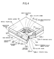
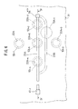
- Fig.4 and Fig.5 show a partially exposed isometric view and a cross-sectional view, respectively, of a first embodiment of a BGA type semiconductor device 30 according to the present invention.
- the BGA type semiconductor device 30 includes an assembly board 31, a semiconductor chip 32, a dam member 33, a metal plate 34, and solder balls 13A.
- the semiconductor chip 32 has solder bumps 40 on a surface 32a thereof.
- the semiconductor chip 32 is fixed with its face down to a central portion of the assembly board 31 by a flip-chip method soldering the solder bumps 40 with pads 41 on the assembly board 31.
- the dam member 33 is formed from the same material as that of the assembly board 31, and has a shape of a rectangular frame. The dam member 33 is adhered to a perimeter area of the assembly board 31.
- the metal plate 34 is adhered to the dam member 33 at a peripheral area of a lower surface thereof so as to cover the semiconductor chip 32. Thus, a space 42 of the semiconductor device 30 containing the semiconductor chip 32 is sealed.
- a paste layer 43 is provided between a back (upper) surface 32b of the semiconductor chip 32 and the metal plate.
- the paste layer 43 is formed from an insulating paste having a high heat transfer characteristic which is supplemented by fillers such as AlN, diamond, and the like.
- Another paste layer 44 is provided between the semiconductor chip 32 and the assembly board 31.
- the paste layer 44 is formed from an insulating paste having a high heat transfer characteristic.
- Each of the solder bumps 40 of the semiconductor chip 32 is electrically connected with a corresponding one of the solder balls 13A.
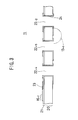
- Fig.6 and Fig.7 are an enlarged plan view and a cross-sectional view, respectively, of the assembly board 31.
- the assembly board 31 includes a printed board 50 as a board base and an additive layer 51 provided on the printed board 50.
- the additive layer 51 includes a wiring pattern 23A.
- Through-holes 22A 1 to 22A 5 are formed only through the printed board 50, and have through-hole inner layer 24A 1 to 24A 5 made of Cu. Also, each of the through-holes 22A 1 to 22A 5 is filled with a filling core 52 formed from a synthetic resin.
- the additive layer 51 is formed on the printed board 50 at an area other than the through-holes 22A 1 to 22A 5 , and is formed on a upper surface 52a of the filling core 52 at the through-holes 22A 1 to 22A 5 . Portions of the additive layer 51 which are directly above the through-holes 22A 1 to 22A 5 are shown as through-hole portions 53 1 to 53 5 .
- the additive layer 51 does not have an opening, paths of wiring patterns can be laid on any place of the additive layer 51. In other words, there is a wider scope for the formation of wiring patterns without a restriction posed by through-holes 22A 1 to 22A 5 , as compared to the related art.
- a wiring pattern 23A is formed to traverse the through-hole portions 53 4 , 53 5 , and 53 2 .
- One end of the wiring pattern 23A is coupled to the through-hole inner layer 24A 2 via a via 54.
- a wiring pattern 23B would have to get around the through-holes as shown by dotted lines in Fig.6.
- the wiring pattern 23A in the case of the present invention is straight, and, thus, has a path of the shortest length.
- solder bump 40 1 of the semiconductor chip 32 is electrically connected to the solder ball 13A 1 beneath the assembly board 31 via the pad 41 1 , the wiring pattern 23A, the via 54, and the through-hole inner layer 24A 2 .
- the semiconductor device 30 is implemented on a printed board (not shown) via the solder bumps 13A.
- the wiring pattern 23A is laid on the shortest path, and there is no wire used in the flip-chip method. Thus, signals having a high frequency can be conducted well without a distortion. Thus, the semiconductor device 30 has a desirable characteristic regarding high frequency signals.
- heat generated by the semiconductor chip 32 is conducted to the metal plate 34 via the paste layer 43, which path is shown by an arrow 60. Then, this heat is extended within the metal plate 34 as shown by arrows 61, and is released into the air as shown by arrows 62.
- heat generated by the semiconductor chip 32 is transferred to the assembly board 31 via the paste layer 44, which path is shown by an arrow 70. Then, this heat is released into air as shown by arrows 72 after extending within the assembly board 31 as shown by arrows 71.
- heat resistance within the semiconductor device 30 is smaller than that of the semiconductor device 10 of Fig.1, so that heat produced by the semiconductor chip 32 can be released more effectively than in the related art.
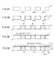
- a through-hole forming process 80 is carried out to create the through-hole.
- a through-hole inner layer forming process 81 is carried out, as shown in Fig.8B, to form the through-hole inner layer 24A 2 , 24A 4 , and 24A 5 by plating Cu and etching the Cu plate.
- a through-hole filling process 82 is carried out to fill a synthetic resin in the through-holes 22A 2 , 22A 4 , and 22A 5 , as shown in Fig.8C. All the through-holes 22A 2 , 22A 4 , and 22A 5 are filled to create the filling core 52.
- an insulator layer forming process 83 is performed in order to form the additive layer 51.
- an insulator layer 56 is formed completely over the printed board 50 including portions of the through-holes.
- the via-hole 57 is formed through the insulator layer 56 at a predetermined location.
- a wiring pattern forming process 84 is performed. This is done by plating Cu and etching the Cu plate so as to form the via 54 and the wiring pattern 23A as shown in Fig.8E. Finally, gold (Au) is plated on the surface.
- Fig.9 shows a second embodiment of a BGA type semiconductor device 90 according to the present invention.
- a metal plate 34A has a rectangular opening 91 at the center thereof.
- the rectangular opening 91 is smaller than the semiconductor chip 32.
- a portion of the lower surface of the metal plate 34A around the opening 91 is adhered to the semiconductor chip 32 at an edge proximity thereof. Thus, a space 42 is sealed.
- a back surface 32b of the semiconductor chip 32 is exposed to air, so that heat generated by the semiconductor chip 32 can be released into air as shown by an arrow 92.
- an inside heat resistance of the semiconductor chip 90 is smaller than that of the semiconductor chip 30 of Fig.4.
- Fig.10 shows a third embodiment of a BGA type semiconductor device 100 according to the present invention.
- the semiconductor device 100 differs from the semiconductor device 90 of the second embodiment only in an additional heat releasing fin 101.
- the heat releasing fin 101 has a portion fitted into the opening 91, and is adhered to the back surface 32b of the semiconductor chip 32 with a paste layer 102 having a high heat transfer rate.
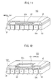
- Fig.11 shows a fourth embodiment of a BGA type semiconductor device 110 according to the present invention.
- the semiconductor device 110 uses a metal cap 111 instead of the dam member 33 and the metal plate 34 of Fig.4.
- the metal cap 111 is adhered to the back surface 32b of the semiconductor chip 32 and to the perimeter area of the upper surface of the assembly board 31.
- the semiconductor device 110 can be constructed with a fewer number of components, compared to the semiconductor device 30 of Fig.4. Yet, the semiconductor device 110 has an inside heat resistance as small as that of the semiconductor device 30.
- Fig.12 shows a fifth embodiment of a BGA type semiconductor device 120 according to the present invention.
- the cap 111A has a rectangular opening 121, which has a smaller size than the semiconductor chip 32.
- the back surface 32b of the semiconductor chip 32 is exposed to air in order to better release heat.
- Fig.13 shows a sixth embodiment of a BGA type semiconductor device 130 according to the present invention.
- the semiconductor device 130 has a heat releasing fin 101.
- the remainder of the device is the same as the semiconductor device 120 of the fifth embodiment.
- the heat releasing fin 101 is partly fitted into the opening 91 so as to be adhered to the back surface 32b of the semiconductor chip 32.
- the adhesion is provided by a paste layer 102 having a high heat transfer rate.
- Fig.14 shows a seventh embodiment of a BGA type semiconductor device 140 according to the present invention.
- the semiconductor chip 32A is provided by a face-up bonding technique. There are wires 140 coupling the semiconductor chip 32A with the assembly board 31.
- a resin package 141 covers the semiconductor chip 32A and the wires 140 to seal those elements. The resin package 141 is formed by putting the resin inside the dam member 33.
- Fig.15 shows an eighth embodiment of a BGA type semiconductor device 150 according to the present invention.
- the semiconductor device 150 has such a structure that a heat releasing fin 151 is provided on the semiconductor device 140 of the seventh embodiment.
- the heat releasing fin 151 is adhered to the upper surface of the resin package 141 by the paste layer 152 having a high heat transfer rate.
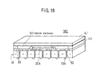
- Fig.16 shows a ninth embodiment of a BGA type semiconductor device 160 according to the present invention.
- the semiconductor device 160 has a structure such that a metal plate 161 is provided on the semiconductor device 140 of the seventh embodiment.
- the metal plate 161 is adhered to the upper surface of the resin package 141 by the paste layer 152 having a high heat transfer rate.
- solder bumps instead of the solder bumps 40 may be provided on the surface 32a of the semiconductor chip 32. Also, pins may be used, replacing the solder balls 13A.
- the paste layer 43 instead of the paste layer 43, a film having a high heat transfer rate may be used. Or the paste layer 43 may include Ag as a filler.
- the additive layer 151 may have a two-layer structure.
- an anisotropic conductive resin may be used instead of the insulating paste having a high heat transfer rate used for the paste layer 44. Also, the insulating paste may be used for forming the dam, replacing the dam member 33.
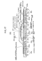
- Fig.17 shows a cross-sectional view of a tenth embodiment of a semiconductor device 200 according to the present invention.
- the semiconductor device 200 includes a semiconductor chip 201, a board 202, a sealing resin 203, external-connection balls 204, and a conductive member 205.
- the semiconductor chip 201 is provided with internal-connection bumps 206 on a lower surface thereof, which are used as first electrodes to be connected to the board 202.
- the internal-connection bumps 206 are formed from solder, for example.
- the other (upper) surface of the semiconductor chip 201 is provided with an upper electrodes 206 which are used as a second electrode.
- the upper electrode 207 is used as a ground electrode.
- the board 202 is a multi-layered printed board which includes wiring layers 202a inside an insulating layer 202b made of glass-epoxy and the like. External-connection wirings 209 having a predetermined pattern are formed on an upper surface of the board 202.
- the external-connection wirings 209 include first external-connection wirings 209a serving as signal lines and power lines, and second external-connection wirings 209b serving as ground lines.
- the semiconductor chip 201 is mounted on the board 202 by means of a flip-chip method.
- inner ends of the first external-connection wirings 209a are connected to the internal-connection bumps 206 of the semiconductor chip 201.
- inner ends of the second external-connection wirings 209b are connected to the upper electrode 207 of the semiconductor chip 201 via the conductive member 205.
- the external-connection wirings 209 and the wiring layers 202a are lead to a back surface of the board 202 through vias 210 formed across layers inside the board 202.
- the vias 210 are connected to the external-connection balls 204, which may be formed from solder, for example.
- the external-connection balls 204 can be formed by arranging solder balls or arranging copper balls plated with solder. Or the external-connection balls 204 can be formed by applying heat-reflow treatment to solder paste which are arranged in predetermined locations by a screen-printing method.
- the sealing resin 203 is formed to cover the conductive member 205 which is provided so as to cover the semiconductor chip 201.
- the sealing resin 203 serves to protect the semiconductor chip 201. Epoxy resin and the like may be used for the sealing resin 203.
- the conductive member 205 is also a novel point of this embodiment, and is formed from silver paste, for example.
- the conductive member 205 is formed by potting the silver paste so as to cover the semiconductor chip 201.
- the conductive member 205 is electrically connected to the upper electrode 207 formed on the upper surface of the semiconductor chip 201. Furthermore, the conductive member 205 is electrically connected to the second external-connection wirings 209b at the upper surface of the board 202. Thus, the semiconductor chip 201 and the second external-connection wirings 209b are electrically connected with each other via the conductive member 205.
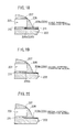
- Fig.18 through Fig.20 show structures of electrical connections between the semiconductor chip 201 and the external-connection wirings 209.
- the sealing resin 203, the wiring layers 202a, and the external-connection balls 204 are omitted for the sake of clarity.
- Fig.15 shows a structure of an electrical connection between the internal-connection bump 206a formed on a signal pad of the semiconductor chip 201 and the first external-connection wirings 209a.
- an insulating member 211 is provided between the semiconductor chip 201 and the board 202. Also, the insulating member 211 is formed on the first external-connection wirings 209a at a connection point between the internal-connection bump 206a formed on the signal pad and the first external-connection wirings 209a.
- the insulating member 211 electrically separates the first external-connection wirings 209a from the conductive member 205.
- the upper electrode (ground electrode) 207 connected to the conductive member 205 is never short-circuited to the first external-connection wirings 209a for conducting signals.
- the insulating member 211 is formed from a resin which is a plastic, soft material. When heat is applied, stress is generated between the semiconductor chip 201 and the board 202 because of a difference in thermal-expansion coefficients of these two elements. However, the insulating member 211 can absorb the stress, thus enhancing the reliability of the semiconductor device 200.
- Fig.16 shows a structure of an electrical connection between the internal-connection bump 206b formed on a ground pad of the semiconductor chip 201 and the second external-connection wirings 209a.
- an insulating member 211 is not formed on the second external-connection wirings 209b at a connection point between the internal-connection bump 206b formed on the ground pad and the second external-connection wirings 209b.
- the second external-connection wirings 209b are exposed to the conductive member 205.
- the insulating member 205 is electrically connected with the second external-connection wirings 209b and the internal-connection bump 206b.
- the insulating member 205 is electrically connected to the upper electrode 207 formed on the upper surface of the semiconductor chip 201, to the internal-connection bump 206b formed beneath the lower surface of the semiconductor chip 201, and to the second external-connection wirings 209b.
- the conductive member 205, the upper electrode 207, the internal-connection bump 206b, and the second external-connection wirings 209b are kept to the same ground level.
- the conductive member 205 has such a large volume that its inductance is lower than a wire connection.
- the electrical connection between the semiconductor chip 201 and the second external-connection wirings 209b can have a suitable characteristic.
- the ground electrode is provided as the upper electrode 207 on the upper surface of the semiconductor chip 201.
- the ground electrode can also be provided beneath the lower surface of the semiconductor chip 201 as is the internal-connection bump 206b.
- Fig.20 shows a structure of an electrical connection between the upper electrode 207 formed on the semiconductor chip 201 and the second external-connection wirings 209b at a location where no internal-connection bump 206 is provided.
- the conductive member 205 electrically connecting the upper electrode 207 and the second external-connection wirings 209b is not limited to a location where the internal-connection bump 206b is provided on the ground pad. That is, the conductive member 205 is also provided where no internal-connection bump 206 is formed. As in the above, the insulating member 211 is removed from the point of connection between the conductive member 205 and the second external-connection wirings 209b.
- the upper electrode 207 formed on the semiconductor chip 201 can be connected to the second external-connection wirings 209b without relying on the internal-connection bump 206 for providing the connection.
- the internal-connection bump 206 can be connected to the conductive member 205, but is not essential for establishing the electrical connection between the upper electrode 207 and the second external-connection wirings 209b.
- the number of the internal-connection bumps 206 provided beneath the lower surface of the semiconductor chip 201 can be reduced. This leads to an extra space being provided for the arrangement of the internal-connection bumps 206.
- the second external-connection wirings 209b can be formed at any location on the board 202 as long as the conductive member 205 is provided at that location. This means that there is a wider scope for the arrangement of the second external-connection wirings 209b.
- the second external-connection wirings 209b can be formed at locations where the first external-connection wirings 209a are not provided.
- the second external-connection wirings 209b can be arranged without a strenuous effort.
- the manufacturing of the semiconductor device 200 can be easier, which leads to an improved yield.
- the conductive member 205 which is connected to the ground electrode and covers the semiconductor chip 201 can serve as a shielding member for the semiconductor chip 201.
- the shielding of the semiconductor chip 201 can be ensured, which leads to prevention of the malfunctions of the semiconductor chip 201.
- the tenth embodiment has been described particularly with regard to a configuration in which the conductive member 205 serving as a ground wiring is connected with the upper electrode 207 serving as the ground electrode and with the internal-connection bump 206b.
- another configuration may be employed in which the conductive member 205 is connected to the power electrodes or the signal electrodes.
- Fig.21 shows a cross-sectional view of an eleventh embodiment of a semiconductor device 220 according to the present invention.
- the same element as those of Fig.17 are referred by the same numerals.
- the board 202 is a multi-layered printed wiring board in which the wiring layers 202a and the vias 210 are formed inside the insulating layer 202b made of glass-epoxy.
- the eleventh embodiment is characterized in that a multi-layered ceramic wiring board 221 and a metal board 222 are used as boards.
- the semiconductor device 220 includes the semiconductor chip 201, the multi-layered ceramic wiring board 221, the metal board 222, a cap 223, the external-connection balls 204, and the conductive member 205.
- the multi-layered ceramic wiring board 221 includes wiring layers 221a and vias 221b connecting between the wiring layers 221a. Furthermore, the external-connection balls 204 are provided beneath the lower surface of the multi-layered ceramic wiring board 221, and are electrically connected to the relevant wiring layers 221a via the vias 221b.
- a cavity 225 is formed at a general center of the multi-layered ceramic wiring board 221, and houses the semiconductor chip 201.
- An opening of the cavity 225 is provided with the cap 223 made of metal, which is fixed by means of a connection member 226. The cap 223 seals the cavity 225.
- the external-connection wirings 209 are provided beneath the lower surface of the insulating layer 224.
- the internal-connection bumps 206 are connected to the external-connection wirings 209 so that the semiconductor chip 201 is connected to the metal board 222 by means of a flip-chip method.
- the multi-layered ceramic wiring board 221 is fixed with an adhesive and the like on one side of the metal board 222 where the semiconductor chip 201 is provided.
- the upper electrode 207 is formed on the surface of the semiconductor chip 201 opposite the surface on which the internal-connection bumps 206 are formed. In this embodiment, the upper electrode 207 is electrically connected to the external-connection wirings 209 via the conductive member 205 as in the previous embodiment.
- the conductive member 205 can be used for electrically connecting the upper electrode 207 and the external-connection wirings 209. Accordingly, there is a wider scope for the arrangement of the internal-connection bumps 206 and the external-connection wirings 209. Thus, the manufacturing of the semiconductor device 220 can become easier, which leads to an improved yield at a time of implementation.
- Fig.22 shows a cross-sectional view of an twelfth embodiment of a semiconductor device 230 according to the present invention.
- the same element as those of Fig.17 are referred by the same numerals.
- a plurality (four in the figure) of semiconductor chips 201A through 201D are packaged and provided on a wiring board 231.
- the twelfth embodiment is characterized in that the semiconductor device 230 is made into a multi-chip module (MCM).
- MCM multi-chip module
- the semiconductor device 230 includes the semiconductor chips 201A through 201D, the wiring board 231, a ceramic board 232, leads 233, a cap 236, and the conductive member 205.
- the wiring board 231 is provided at an upper surface thereof with external-connection wirings (not shown), and the semiconductor chips 201A through 201D are connected to the wiring board 231 by means of a flip-chip method.
- the insulating member 211 is provided between each of the semiconductor chips 201A through 201D and the wiring board 231.
- some of the internal-connection bumps 206A through 206D are appropriately insulated from the conductive member 205.
- the wiring board 231 is mounted on the ceramic board 232, whose perimeter is provided with a ceramic frame 234 having a frame shape.
- the leads 233 are fixed between the ceramic board 232 and the ceramic frame 234.
- An inner lead portion 233a of the leads 233 is electrically connected to the external-connection wirings formed on the wiring board 231 via wires 235.
- the cap 236 is provided at an upper opening of the ceramic frame 234, sealing the semiconductor chips 201A through 201D.
- Upper electrodes 207A through 207D are, respectively, formed on the surfaces of the semiconductor chips 201A through 201D opposite the surfaces on which the internal-connection bumps 206A through 206D are formed.
- the upper electrodes 207A through 207D are electrically connected to the external-connection wirings via the conductive member 205 as in the previous embodiments.
- the upper electrodes 207A through 207D formed on the semiconductor chip 201A through 201D, respectively, are kept to the same voltage level (e.g., the ground level).
- the upper electrodes 207A through 207D can be connected to the external-connection wirings via the conductive member 205.
- the manufacturing of the semiconductor device 230 can be made easier, and the yield at a time of the implementation can be improved.
- Fig.23 shows a cross-sectional view of a thirteenth embodiment of a semiconductor device 240 according to the present invention.
- the same elements as those of Fig.17 are referred by the same numerals.
- This embodiment is characterized in that the semiconductor device 240 has a chip-on-chip structure by piling two semiconductor chips 201 and 241 one over the other.
- the semiconductor device 240 includes the semiconductor chips 201 and 241, the board 202, an insulating member 242, the sealing resin 203, the external-connection balls 204, and the conductive member 205.
- the semiconductor chip 241 is electrically connected to the external-connection wirings 209 formed on the board 202 via wires 243. Electrodes (not shown) are provided on an upper surface of the semiconductor chip 241, and are electrically connected to the semiconductor chip 201. These electrodes are connected to the internal-connection bumps 206 formed on the semiconductor chip 201, so that the semiconductor chip 201 is connected to the upper surface of the semiconductor chip 241 by means of a flip-chip method. Thus, the semiconductor chip 201 ends up being mounted on the semiconductor chip 241.
- the insulating layer 242 is provided to cover the semiconductor chip 241 and to cover part of the semiconductor chip 201.
- the points of electrical connection between the semiconductor chips 201 and 241 are insulated from the conductive member 205.
- the sealing resin 203 is provided to cover an upper surface of the conductive member 205.
- the upper electrode 207 is provided on the surface of the semiconductor chip 201 opposite the surface on which the internal-connection bumps 206 are formed.
- the upper electrode 207 is electrically connected to the external-connection wirings 209b formed on the board 202 via the conductive member 205.
- the upper electrode 207 can be connected to the external-connection wirings 209b via the conductive member 205.
- the manufacturing of the semiconductor device 240 can be made easier, and the yield at a time of the implementation can be improved.
- the semiconductor device according to the present invention can provide a wiring pattern on the additive layer without a restriction posed by the through-holes.
- a wiring pattern traversing through-holes can be laid on the additive layer.
- the path length of wiring patterns in the semiconductor devices having nodes beneath an assembly board can be reduced when compared with the case of the related art.
- a better signal propagation characteristic can be obtained for signals having a high frequency.
- the semiconductor device according to the present invention can lower an inside heat resistance, compared to semiconductor devices of the related art.
- the semiconductor device of the present invention can enhance a heat releasing characteristic, yet can properly seal the semiconductor chip inside.
- the semiconductor device according to the present invention can reduce the density of electrode arrangement, compared to a configuration in which all the electrodes are provided on the same surface of the semiconductor chip.
- the external-connection nodes can be arranged with a high density so as to be easily manufactured, leading to an improved yield.
- the semiconductor device has the conductive member covering the semiconductor chip, so that the low inductance of the conductive member can provide better electrical characteristics. Also, when the conductive member is coupled to the ground level, the conductive member can serve as a shield for the semiconductor chip.
- the semiconductor device according to the present invention can electrically connect the external-connection wirings with appropriate electrodes of the semiconductor chip via the conductive member.
- the semiconductor device according to the present invention can electrically connect the external-connection wirings with appropriate electrodes of the semiconductor chip via the conductive member.
- the semiconductor chip according to the present invention provides the insulating member which can properly insulate the internal-connection bumps from each other or from the conductive member.
- the present invention can be applied to the multi-chip module structure.
- the present invention can be applied to the chip-on-chip structure.
Landscapes
- Engineering & Computer Science (AREA)
- Manufacturing & Machinery (AREA)
- Microelectronics & Electronic Packaging (AREA)
- Structures Or Materials For Encapsulating Or Coating Semiconductor Devices Or Solid State Devices (AREA)
- Wire Bonding (AREA)
- Insulated Metal Substrates For Printed Circuits (AREA)
- Cooling Or The Like Of Semiconductors Or Solid State Devices (AREA)
Applications Claiming Priority (3)
| Application Number | Priority Date | Filing Date | Title |
|---|---|---|---|
| JP9215594 | 1994-04-28 | ||
| JP7059562A JP3034180B2 (ja) | 1994-04-28 | 1995-03-17 | 半導体装置及びその製造方法及び基板 |
| EP95105640A EP0685878B1 (de) | 1994-04-28 | 1995-04-13 | Halbleiterbauelement und Verfahren zu seiner Herstellung |
Related Parent Applications (2)
| Application Number | Title | Priority Date | Filing Date |
|---|---|---|---|
| EP95105640A Division EP0685878B1 (de) | 1994-04-28 | 1995-04-13 | Halbleiterbauelement und Verfahren zu seiner Herstellung |
| EP95105640.7 Division | 1995-04-13 |
Publications (2)
| Publication Number | Publication Date |
|---|---|
| EP1715512A2 true EP1715512A2 (de) | 2006-10-25 |
| EP1715512A3 EP1715512A3 (de) | 2013-02-13 |
Family
ID=26400610
Family Applications (4)
| Application Number | Title | Priority Date | Filing Date |
|---|---|---|---|
| EP01129844A Withdrawn EP1198000A1 (de) | 1994-04-28 | 1995-04-13 | Halbleitervorrichtung und Aufbauplatte |
| EP06116868A Withdrawn EP1715512A3 (de) | 1994-04-28 | 1995-04-13 | Halbleitervorrichtung und ein Verfahren dessen Herstellung |
| EP95105640A Expired - Lifetime EP0685878B1 (de) | 1994-04-28 | 1995-04-13 | Halbleiterbauelement und Verfahren zu seiner Herstellung |
| EP99101351A Ceased EP0915504A1 (de) | 1994-04-28 | 1995-04-13 | Halbleiterverpackung und deren Herstellungsverfahren |
Family Applications Before (1)
| Application Number | Title | Priority Date | Filing Date |
|---|---|---|---|
| EP01129844A Withdrawn EP1198000A1 (de) | 1994-04-28 | 1995-04-13 | Halbleitervorrichtung und Aufbauplatte |
Family Applications After (2)
| Application Number | Title | Priority Date | Filing Date |
|---|---|---|---|
| EP95105640A Expired - Lifetime EP0685878B1 (de) | 1994-04-28 | 1995-04-13 | Halbleiterbauelement und Verfahren zu seiner Herstellung |
| EP99101351A Ceased EP0915504A1 (de) | 1994-04-28 | 1995-04-13 | Halbleiterverpackung und deren Herstellungsverfahren |
Country Status (6)
| Country | Link |
|---|---|
| US (4) | US5729435A (de) |
| EP (4) | EP1198000A1 (de) |
| JP (1) | JP3034180B2 (de) |
| KR (1) | KR100199437B1 (de) |
| DE (1) | DE69536084D1 (de) |
| TW (2) | TW559338U (de) |
Families Citing this family (52)
| Publication number | Priority date | Publication date | Assignee | Title |
|---|---|---|---|---|
| JP3034180B2 (ja) * | 1994-04-28 | 2000-04-17 | 富士通株式会社 | 半導体装置及びその製造方法及び基板 |
| KR100386061B1 (ko) | 1995-10-24 | 2003-08-21 | 오끼 덴끼 고오교 가부시끼가이샤 | 크랙을방지하기위한개량된구조를가지는반도체장치및리이드프레임 |
| US6734545B1 (en) * | 1995-11-29 | 2004-05-11 | Hitachi, Ltd. | BGA type semiconductor device and electronic equipment using the same |
| DE19546045C1 (de) * | 1995-12-09 | 1997-05-22 | Bosch Gmbh Robert | Flip-Chip-Verfahren zur Herstellung eines Multichip-Moduls |
| US6209665B1 (en) * | 1996-07-01 | 2001-04-03 | Ardis L. Holte | Reverse circulation drilling system with bit locked underreamer arms |
| US5798557A (en) * | 1996-08-29 | 1998-08-25 | Harris Corporation | Lid wafer bond packaging and micromachining |
| JP3475426B2 (ja) * | 1997-03-24 | 2003-12-08 | セイコーエプソン株式会社 | 半導体装置の製造方法 |
| US6317333B1 (en) * | 1997-08-28 | 2001-11-13 | Mitsubishi Denki Kabushiki Kaisha | Package construction of semiconductor device |
| US5965944A (en) * | 1997-11-12 | 1999-10-12 | International Business Machines Corporation | Printed circuit boards for mounting a semiconductor integrated circuit die |
| JP3579740B2 (ja) * | 1998-04-18 | 2004-10-20 | Tdk株式会社 | 電子部品の製造方法 |
| US6049136A (en) * | 1998-06-03 | 2000-04-11 | Hewlett-Packard Company | Integrated circuit having unique lead configuration |
| RU2134466C1 (ru) * | 1998-12-08 | 1999-08-10 | Таран Александр Иванович | Носитель кристалла ис |
| JP3287408B2 (ja) * | 1999-06-16 | 2002-06-04 | 日本電気株式会社 | 半導体装置および半導体基板貫通導体の形成方法 |
| JP2001077500A (ja) * | 1999-06-30 | 2001-03-23 | Murata Mfg Co Ltd | 電子部品、誘電体フィルタ、誘電体デュプレクサ、および電子部品の製造方法 |
| DE10002852A1 (de) * | 2000-01-24 | 2001-08-02 | Infineon Technologies Ag | Abschirmeinrichtung und elektrisches Bauteil mit einer Abschirmeinrichtung |
| US6465858B2 (en) * | 2000-03-24 | 2002-10-15 | Matsushita Electric Industrial Co., Ltd. | Semiconductor device package for optical communication device |
| CN1444839A (zh) * | 2000-05-31 | 2003-09-24 | Ttm先进电路公司 | 填充方法 |
| CN1444840A (zh) | 2000-05-31 | 2003-09-24 | 霍尼韦尔国际公司 | 填充装置 |
| US6855385B2 (en) * | 2000-05-31 | 2005-02-15 | Ttm Advanced Circuits, Inc. | PCB support plate for PCB via fill |
| US6506332B2 (en) * | 2000-05-31 | 2003-01-14 | Honeywell International Inc. | Filling method |
| US6800232B2 (en) * | 2000-05-31 | 2004-10-05 | Ttm Advanced Circuits, Inc. | PCB support plate method for PCB via fill |
| US6417563B1 (en) * | 2000-07-14 | 2002-07-09 | Advanced Micro Devices, Inc. | Spring frame for protecting packaged electronic devices |
| US6653730B2 (en) | 2000-12-14 | 2003-11-25 | Intel Corporation | Electronic assembly with high capacity thermal interface |
| US20030009878A1 (en) * | 2001-07-12 | 2003-01-16 | John Gregory | Method for attaching an electronic component to a substrate |
| US6927471B2 (en) * | 2001-09-07 | 2005-08-09 | Peter C. Salmon | Electronic system modules and method of fabrication |
| US7297572B2 (en) * | 2001-09-07 | 2007-11-20 | Hynix Semiconductor, Inc. | Fabrication method for electronic system modules |
| US6495926B1 (en) * | 2001-11-29 | 2002-12-17 | Sun Microsystems, Inc. | 60 degree bump placement layout for an integrated circuit power grid |
| KR100499003B1 (ko) * | 2002-12-12 | 2005-07-01 | 삼성전기주식회사 | 도금 인입선을 사용하지 않는 패키지 기판 및 그 제조 방법 |
| CA2455024A1 (en) * | 2003-01-30 | 2004-07-30 | Endicott Interconnect Technologies, Inc. | Stacked chip electronic package having laminate carrier and method of making same |
| US7035113B2 (en) * | 2003-01-30 | 2006-04-25 | Endicott Interconnect Technologies, Inc. | Multi-chip electronic package having laminate carrier and method of making same |
| US7109573B2 (en) * | 2003-06-10 | 2006-09-19 | Nokia Corporation | Thermally enhanced component substrate |
| FR2884047A1 (fr) * | 2005-03-31 | 2006-10-06 | Intexys Sa | Procede et dispositif d'encapsulation de composants electroniques et optoelectroniques |
| JP4611010B2 (ja) * | 2004-12-10 | 2011-01-12 | 日立ビアメカニクス株式会社 | 多層回路基板の製造方法 |
| TWI246760B (en) * | 2004-12-22 | 2006-01-01 | Siliconware Precision Industries Co Ltd | Heat dissipating semiconductor package and fabrication method thereof |
| JP4860994B2 (ja) * | 2005-12-06 | 2012-01-25 | ルネサスエレクトロニクス株式会社 | 半導体装置 |
| US8181429B2 (en) * | 2005-12-21 | 2012-05-22 | Toyo Seikan Kaisha, Ltd. | Method of producing contents filed in a container |
| US7607355B2 (en) * | 2007-02-16 | 2009-10-27 | Yamaha Corporation | Semiconductor device |
| US7561430B2 (en) * | 2007-04-30 | 2009-07-14 | Watlow Electric Manufacturing Company | Heat management system for a power switching device |
| US8426960B2 (en) * | 2007-12-21 | 2013-04-23 | Alpha & Omega Semiconductor, Inc. | Wafer level chip scale packaging |
| JP4833307B2 (ja) * | 2009-02-24 | 2011-12-07 | インターナショナル・ビジネス・マシーンズ・コーポレーション | 半導体モジュール、端子板、端子板の製造方法および半導体モジュールの製造方法 |
| KR100935854B1 (ko) | 2009-09-22 | 2010-01-08 | 테세라 리써치 엘엘씨 | 와이어 본딩 및 기준 와이어 본딩에 의해 제어되는 임피던스를 가진 마이크로전자 어셈블리 |
| KR100950511B1 (ko) | 2009-09-22 | 2010-03-30 | 테세라 리써치 엘엘씨 | 와이어 본딩 및 도전성 기준 소자에 의해 제어되는 임피던스를 포함하는 마이크로전자 어셈블리 |
| US8618654B2 (en) * | 2010-07-20 | 2013-12-31 | Marvell World Trade Ltd. | Structures embedded within core material and methods of manufacturing thereof |
| GB2481836B (en) * | 2010-07-08 | 2012-06-13 | Keymat Technology Ltd | Circuit board connector with drilling tamper detection arrangement |
| US8786083B2 (en) | 2010-09-16 | 2014-07-22 | Tessera, Inc. | Impedance controlled packages with metal sheet or 2-layer RDL |
| US8853708B2 (en) | 2010-09-16 | 2014-10-07 | Tessera, Inc. | Stacked multi-die packages with impedance control |
| US8581377B2 (en) | 2010-09-16 | 2013-11-12 | Tessera, Inc. | TSOP with impedance control |
| US9136197B2 (en) | 2010-09-16 | 2015-09-15 | Tessera, Inc. | Impedence controlled packages with metal sheet or 2-layer RDL |
| US8847412B2 (en) * | 2012-11-09 | 2014-09-30 | Invensas Corporation | Microelectronic assembly with thermally and electrically conductive underfill |
| KR101603285B1 (ko) | 2014-03-24 | 2016-03-14 | 대남환경 주식회사 | 해상 오일 방제선 |
| CN107949188A (zh) * | 2017-11-16 | 2018-04-20 | 广东兴达鸿业电子有限公司 | 具有npth连孔的电路板加工方法 |
| CN119764299B (zh) * | 2024-12-23 | 2025-11-14 | 广东全芯半导体有限公司 | 一种具有电磁屏蔽功能的半导体封装结构 |
Family Cites Families (41)
| Publication number | Priority date | Publication date | Assignee | Title |
|---|---|---|---|---|
| US4050756A (en) * | 1975-12-22 | 1977-09-27 | International Telephone And Telegraph Corporation | Conductive elastomer connector and method of making same |
| US4218701A (en) | 1978-07-24 | 1980-08-19 | Citizen Watch Co., Ltd. | Package for an integrated circuit having a container with support bars |
| US4322778A (en) * | 1980-01-25 | 1982-03-30 | International Business Machines Corp. | High performance semiconductor package assembly |
| US4483067A (en) * | 1981-09-11 | 1984-11-20 | U.S. Philips Corporation | Method of manufacturing an identification card and an identification manufactured, for example, by this method |
| JPS58220451A (ja) * | 1982-06-17 | 1983-12-22 | Kyodo Printing Co Ltd | Icモジユ−ル |
| JPS5999752A (ja) * | 1982-11-29 | 1984-06-08 | Toshiba Corp | 混成集積回路装置 |
| JPS60134446A (ja) * | 1983-12-23 | 1985-07-17 | Hitachi Ltd | 半導体装置 |
| FR2575331B1 (fr) * | 1984-12-21 | 1987-06-05 | Labo Electronique Physique | Boitier pour composant electronique |
| FR2584235B1 (fr) * | 1985-06-26 | 1988-04-22 | Bull Sa | Procede de montage d'un circuit integre sur un support, dispositif en resultant et son application a une carte a microcircuits electroniques |
| DE3685647T2 (de) * | 1985-07-16 | 1993-01-07 | Nippon Telegraph & Telephone | Verbindungskontakte zwischen substraten und verfahren zur herstellung derselben. |
| JPS6253000A (ja) * | 1985-08-31 | 1987-03-07 | 日本電気株式会社 | 半導体の実装構造 |
| JPS62136865A (ja) * | 1985-12-11 | 1987-06-19 | Hitachi Ltd | モジユ−ル実装構造 |
| US4843067A (en) * | 1986-11-19 | 1989-06-27 | Yaguang Liu | Polysaccharide containing pharmaceutical composition for increasing the immune function |
| US5138438A (en) * | 1987-06-24 | 1992-08-11 | Akita Electronics Co. Ltd. | Lead connections means for stacked tab packaged IC chips |
| US4978639A (en) * | 1989-01-10 | 1990-12-18 | Avantek, Inc. | Method for the simultaneous formation of via-holes and wraparound plating on semiconductor chips |
| US4954313A (en) | 1989-02-03 | 1990-09-04 | Amdahl Corporation | Method and apparatus for filling high density vias |
| EP0382203B1 (de) * | 1989-02-10 | 1995-04-26 | Fujitsu Limited | Keramische Packung vom Halbleiteranordnungstyp und Verfahren zum Zusammensetzen derselben |
| US4922376A (en) * | 1989-04-10 | 1990-05-01 | Unistructure, Inc. | Spring grid array interconnection for active microelectronic elements |
| US4954878A (en) * | 1989-06-29 | 1990-09-04 | Digital Equipment Corp. | Method of packaging and powering integrated circuit chips and the chip assembly formed thereby |
| JPH0344957A (ja) * | 1989-07-12 | 1991-02-26 | Fujitsu Ltd | 半導体チップ実装用セラミック基板の製造方法 |
| US5200362A (en) * | 1989-09-06 | 1993-04-06 | Motorola, Inc. | Method of attaching conductive traces to an encapsulated semiconductor die using a removable transfer film |
| US4978638A (en) * | 1989-12-21 | 1990-12-18 | International Business Machines Corporation | Method for attaching heat sink to plastic packaged electronic component |
| DE3943087C1 (de) * | 1989-12-27 | 1990-11-29 | Erhard 6900 Heidelberg De Lamberti | |
| NO900229D0 (no) | 1990-01-16 | 1990-01-16 | Micro Electronics Ame A S | Fremgangsmaate for fremstilling av miniatyrisert impedanstilpasset ledningsnett. |
| US5073814A (en) * | 1990-07-02 | 1991-12-17 | General Electric Company | Multi-sublayer dielectric layers |
| JP3057766B2 (ja) * | 1990-12-18 | 2000-07-04 | 日本ケミコン株式会社 | 厚膜多層回路基板及びその製造方法 |
| US5166772A (en) | 1991-02-22 | 1992-11-24 | Motorola, Inc. | Transfer molded semiconductor device package with integral shield |
| JPH04276631A (ja) * | 1991-03-04 | 1992-10-01 | Toshiba Corp | 電界効果トランジスタの製造方法 |
| JP2966972B2 (ja) | 1991-07-05 | 1999-10-25 | 株式会社日立製作所 | 半導体チップキャリアとそれを実装したモジュール及びそれを組み込んだ電子機器 |
| JP2936819B2 (ja) * | 1991-07-24 | 1999-08-23 | 日本電気株式会社 | Icチップの実装構造 |
| JPH0541471A (ja) * | 1991-08-07 | 1993-02-19 | Hitachi Ltd | 半導体集積回路装置 |
| JP2634516B2 (ja) * | 1991-10-15 | 1997-07-30 | 三菱電機株式会社 | 反転型icの製造方法、反転型ic、icモジュール |
| JP2712967B2 (ja) * | 1991-12-19 | 1998-02-16 | 日本電気株式会社 | 半導体装置 |
| CA2089435C (en) * | 1992-02-14 | 1997-12-09 | Kenzi Kobayashi | Semiconductor device |
| JPH05326631A (ja) * | 1992-05-15 | 1993-12-10 | Rohm Co Ltd | 半導体装置の実装構造 |
| EP0598914B1 (de) * | 1992-06-05 | 2000-10-11 | Mitsui Chemicals, Inc. | Dreidimensionale leiterplatte, elektronische bauelementanordnung unter verwendung dieser leiterplatte und herstellungsverfahren zu dieser leiterplatte |
| US5280413A (en) * | 1992-09-17 | 1994-01-18 | Ceridian Corporation | Hermetically sealed circuit modules having conductive cap anchors |
| US5450290A (en) * | 1993-02-01 | 1995-09-12 | International Business Machines Corporation | Printed circuit board with aligned connections and method of making same |
| US5703405A (en) * | 1993-03-15 | 1997-12-30 | Motorola, Inc. | Integrated circuit chip formed from processing two opposing surfaces of a wafer |
| JP3034180B2 (ja) * | 1994-04-28 | 2000-04-17 | 富士通株式会社 | 半導体装置及びその製造方法及び基板 |
| JPH09326142A (ja) * | 1996-06-05 | 1997-12-16 | Matsushita Electric Ind Co Ltd | 電子機器の画面操作装置 |
-
1995
- 1995-03-17 JP JP7059562A patent/JP3034180B2/ja not_active Expired - Lifetime
- 1995-04-13 EP EP01129844A patent/EP1198000A1/de not_active Withdrawn
- 1995-04-13 EP EP06116868A patent/EP1715512A3/de not_active Withdrawn
- 1995-04-13 EP EP95105640A patent/EP0685878B1/de not_active Expired - Lifetime
- 1995-04-13 EP EP99101351A patent/EP0915504A1/de not_active Ceased
- 1995-04-13 DE DE69536084T patent/DE69536084D1/de not_active Expired - Lifetime
- 1995-04-25 KR KR1019950009706A patent/KR100199437B1/ko not_active Expired - Lifetime
- 1995-04-28 TW TW091212186U patent/TW559338U/zh not_active IP Right Cessation
- 1995-04-28 TW TW092209806U patent/TW563902U/zh not_active IP Right Cessation
-
1997
- 1997-01-13 US US08/782,381 patent/US5729435A/en not_active Expired - Lifetime
- 1997-09-08 US US08/924,958 patent/US5978222A/en not_active Expired - Lifetime
-
1998
- 1998-11-18 US US09/195,232 patent/US6088233A/en not_active Expired - Fee Related
-
2000
- 2000-02-18 US US09/506,733 patent/US6184133B1/en not_active Expired - Lifetime
Also Published As
| Publication number | Publication date |
|---|---|
| EP0685878A2 (de) | 1995-12-06 |
| EP1198000A1 (de) | 2002-04-17 |
| JP3034180B2 (ja) | 2000-04-17 |
| TW563902U (en) | 2003-11-21 |
| DE69536084D1 (de) | 2010-08-05 |
| KR100199437B1 (ko) | 1999-06-15 |
| US5978222A (en) | 1999-11-02 |
| US5729435A (en) | 1998-03-17 |
| EP0915504A1 (de) | 1999-05-12 |
| EP0685878B1 (de) | 2010-06-23 |
| US6184133B1 (en) | 2001-02-06 |
| KR950030321A (ko) | 1995-11-24 |
| JPH0817964A (ja) | 1996-01-19 |
| EP1715512A3 (de) | 2013-02-13 |
| US6088233A (en) | 2000-07-11 |
| TW559338U (en) | 2003-10-21 |
| EP0685878A3 (de) | 1996-11-06 |
Similar Documents
| Publication | Publication Date | Title |
|---|---|---|
| US5978222A (en) | Semiconductor device and assembly board having through-holes filled with filling core | |
| US6347037B2 (en) | Semiconductor device and method of forming the same | |
| US6013946A (en) | Wire bond packages for semiconductor chips and related methods and assemblies | |
| US6468834B1 (en) | Method of fabricating a BGA package using PCB and tape in a die-up configuration | |
| US6252298B1 (en) | Semiconductor chip package using flexible circuit board with central opening | |
| US5615089A (en) | BGA semiconductor device including a plurality of semiconductor chips located on upper and lower surfaces of a first substrate | |
| KR100694739B1 (ko) | 다수의 전원/접지면을 갖는 볼 그리드 어레이 패키지 | |
| KR100231276B1 (ko) | 반도체패키지의 구조 및 제조방법 | |
| US6534879B2 (en) | Semiconductor chip and semiconductor device having the chip | |
| US6228683B1 (en) | High density leaded ball-grid array package | |
| JP3123638B2 (ja) | 半導体装置 | |
| US5309021A (en) | Semiconductor device having particular power distribution interconnection arrangement | |
| KR100194747B1 (ko) | 반도체장치 | |
| KR100271676B1 (ko) | 반도체장치용패키지및반도체장치와그들의제조방법 | |
| US20040070948A1 (en) | Cavity-down ball grid array semiconductor package with heat spreader | |
| US6627986B2 (en) | Substrate for semiconductor device and semiconductor device fabrication using the same | |
| JP3450477B2 (ja) | 半導体装置及びその製造方法 | |
| KR100762871B1 (ko) | 칩크기 패키지 제조방법 | |
| JP3645701B2 (ja) | 半導体装置 | |
| KR101185857B1 (ko) | Bga 타입 스택 패키지 및 이를 이용한 멀티 패키지 | |
| KR100487463B1 (ko) | 반도체칩과리드프레임이직접전기적으로접속되는반도체칩패키지소자 | |
| JP3405718B2 (ja) | 半導体装置 | |
| KR100195511B1 (ko) | 리드 프레임을 이용한 볼 그리드 어레이 패키지 | |
| KR100369501B1 (ko) | 반도체패키지 | |
| KR20100078957A (ko) | 반도체 모듈 |
Legal Events
| Date | Code | Title | Description |
|---|---|---|---|
| PUAI | Public reference made under article 153(3) epc to a published international application that has entered the european phase |
Free format text: ORIGINAL CODE: 0009012 |
|
| 17P | Request for examination filed |
Effective date: 20060708 |
|
| AC | Divisional application: reference to earlier application |
Ref document number: 0685878 Country of ref document: EP Kind code of ref document: P |
|
| AK | Designated contracting states |
Kind code of ref document: A2 Designated state(s): DE FR GB |
|
| RAP1 | Party data changed (applicant data changed or rights of an application transferred) |
Owner name: FUJITSU MICROELECTRONICS LIMITED |
|
| RAP1 | Party data changed (applicant data changed or rights of an application transferred) |
Owner name: FUJITSU SEMICONDUCTOR LIMITED |
|
| RIC1 | Information provided on ipc code assigned before grant |
Ipc: H01L 23/367 20060101ALI20120831BHEP Ipc: H01L 23/498 20060101ALI20120831BHEP Ipc: H01L 21/48 20060101AFI20120831BHEP Ipc: H01L 23/538 20060101ALI20120831BHEP Ipc: H01L 21/60 20060101ALI20120831BHEP Ipc: H01L 23/053 20060101ALI20120831BHEP |
|
| PUAL | Search report despatched |
Free format text: ORIGINAL CODE: 0009013 |
|
| AK | Designated contracting states |
Kind code of ref document: A3 Designated state(s): DE FR GB |
|
| RIC1 | Information provided on ipc code assigned before grant |
Ipc: H01L 21/60 20060101ALI20130107BHEP Ipc: H01L 23/498 20060101ALI20130107BHEP Ipc: H01L 23/053 20060101ALI20130107BHEP Ipc: H01L 23/367 20060101ALI20130107BHEP Ipc: H01L 23/538 20060101ALI20130107BHEP Ipc: H01L 21/48 20060101AFI20130107BHEP |
|
| AKX | Designation fees paid |
Designated state(s): DE FR GB |
|
| STAA | Information on the status of an ep patent application or granted ep patent |
Free format text: STATUS: THE APPLICATION IS DEEMED TO BE WITHDRAWN |
|
| 18D | Application deemed to be withdrawn |
Effective date: 20130814 |