EP1720204A1 - Eutektische Bindung mit vorübergehender flüssiger Phase - Google Patents
Eutektische Bindung mit vorübergehender flüssiger Phase Download PDFInfo
- Publication number
- EP1720204A1 EP1720204A1 EP20060112160 EP06112160A EP1720204A1 EP 1720204 A1 EP1720204 A1 EP 1720204A1 EP 20060112160 EP20060112160 EP 20060112160 EP 06112160 A EP06112160 A EP 06112160A EP 1720204 A1 EP1720204 A1 EP 1720204A1
- Authority
- EP
- European Patent Office
- Prior art keywords
- bonding
- eutectic bonding
- eutectic
- component
- materials
- Prior art date
- Legal status (The legal status is an assumption and is not a legal conclusion. Google has not performed a legal analysis and makes no representation as to the accuracy of the status listed.)
- Granted
Links
Images



Classifications
-
- H—ELECTRICITY
- H10—SEMICONDUCTOR DEVICES; ELECTRIC SOLID-STATE DEVICES NOT OTHERWISE PROVIDED FOR
- H10P—GENERIC PROCESSES OR APPARATUS FOR THE MANUFACTURE OR TREATMENT OF DEVICES COVERED BY CLASS H10
- H10P90/00—Preparation of wafers not covered by a single main group of this subclass, e.g. wafer reinforcement
- H10P90/19—Preparing inhomogeneous wafers
- H10P90/1904—Preparing vertically inhomogeneous wafers
- H10P90/1906—Preparing SOI wafers
-
- H—ELECTRICITY
- H10—SEMICONDUCTOR DEVICES; ELECTRIC SOLID-STATE DEVICES NOT OTHERWISE PROVIDED FOR
- H10W—GENERIC PACKAGES, INTERCONNECTIONS, CONNECTORS OR OTHER CONSTRUCTIONAL DETAILS OF DEVICES COVERED BY CLASS H10
- H10W10/00—Isolation regions in semiconductor bodies between components of integrated devices
- H10W10/10—Isolation regions comprising dielectric materials
- H10W10/181—Semiconductor-on-insulator [SOI] isolation regions, e.g. buried oxide regions of SOI wafers
-
- H—ELECTRICITY
- H10—SEMICONDUCTOR DEVICES; ELECTRIC SOLID-STATE DEVICES NOT OTHERWISE PROVIDED FOR
- H10W—GENERIC PACKAGES, INTERCONNECTIONS, CONNECTORS OR OTHER CONSTRUCTIONAL DETAILS OF DEVICES COVERED BY CLASS H10
- H10W72/00—Interconnections or connectors in packages
- H10W72/30—Die-attach connectors
-
- H—ELECTRICITY
- H10—SEMICONDUCTOR DEVICES; ELECTRIC SOLID-STATE DEVICES NOT OTHERWISE PROVIDED FOR
- H10W—GENERIC PACKAGES, INTERCONNECTIONS, CONNECTORS OR OTHER CONSTRUCTIONAL DETAILS OF DEVICES COVERED BY CLASS H10
- H10W72/00—Interconnections or connectors in packages
- H10W72/071—Connecting or disconnecting
- H10W72/073—Connecting or disconnecting of die-attach connectors
- H10W72/07321—Aligning
- H10W72/07327—Aligning involving guiding structures, e.g. spacers or supporting members
-
- H—ELECTRICITY
- H10—SEMICONDUCTOR DEVICES; ELECTRIC SOLID-STATE DEVICES NOT OTHERWISE PROVIDED FOR
- H10W—GENERIC PACKAGES, INTERCONNECTIONS, CONNECTORS OR OTHER CONSTRUCTIONAL DETAILS OF DEVICES COVERED BY CLASS H10
- H10W72/00—Interconnections or connectors in packages
- H10W72/071—Connecting or disconnecting
- H10W72/073—Connecting or disconnecting of die-attach connectors
- H10W72/07331—Connecting techniques
- H10W72/07336—Soldering or alloying
-
- H—ELECTRICITY
- H10—SEMICONDUCTOR DEVICES; ELECTRIC SOLID-STATE DEVICES NOT OTHERWISE PROVIDED FOR
- H10W—GENERIC PACKAGES, INTERCONNECTIONS, CONNECTORS OR OTHER CONSTRUCTIONAL DETAILS OF DEVICES COVERED BY CLASS H10
- H10W72/00—Interconnections or connectors in packages
- H10W72/071—Connecting or disconnecting
- H10W72/073—Connecting or disconnecting of die-attach connectors
- H10W72/07331—Connecting techniques
- H10W72/07337—Connecting techniques using a polymer adhesive, e.g. an adhesive based on silicone or epoxy
-
- Y—GENERAL TAGGING OF NEW TECHNOLOGICAL DEVELOPMENTS; GENERAL TAGGING OF CROSS-SECTIONAL TECHNOLOGIES SPANNING OVER SEVERAL SECTIONS OF THE IPC; TECHNICAL SUBJECTS COVERED BY FORMER USPC CROSS-REFERENCE ART COLLECTIONS [XRACs] AND DIGESTS
- Y10—TECHNICAL SUBJECTS COVERED BY FORMER USPC
- Y10T—TECHNICAL SUBJECTS COVERED BY FORMER US CLASSIFICATION
- Y10T428/00—Stock material or miscellaneous articles
- Y10T428/13—Hollow or container type article [e.g., tube, vase, etc.]
-
- Y—GENERAL TAGGING OF NEW TECHNOLOGICAL DEVELOPMENTS; GENERAL TAGGING OF CROSS-SECTIONAL TECHNOLOGIES SPANNING OVER SEVERAL SECTIONS OF THE IPC; TECHNICAL SUBJECTS COVERED BY FORMER USPC CROSS-REFERENCE ART COLLECTIONS [XRACs] AND DIGESTS
- Y10—TECHNICAL SUBJECTS COVERED BY FORMER USPC
- Y10T—TECHNICAL SUBJECTS COVERED BY FORMER US CLASSIFICATION
- Y10T428/00—Stock material or miscellaneous articles
- Y10T428/31504—Composite [nonstructural laminate]
- Y10T428/31678—Of metal
Definitions
- the present invention is directed to a method for transient liquid phase eutectic bonding and a structure including two components joined together by transient liquid phase eutectic bonding.
- microelectromechanical systems MEMS
- microdevices microstructures and the like
- microstructures it is often desired to join various parts, wafers, portions of wafers, components, substrates and the like together.
- the parts, wafer, portions of wafers, components, substrates and the like that are to be joined together may be relatively large components (i.e. having, for example, a surface area of several inches) but may carry a relatively high number of small microstructures thereon.
- the joint that couples the two components must be sufficiently robust to withstand subsequent processing steps and to withstand environmental conditions to which the assembled structure may be exposed (i.e., high temperatures, corrosive environments, etc.).
- each substrate When coupling two substrates together, each substrate typically has a layer of bonding material located thereon.
- the bonding material on one substrate can react with a bonding material on the other substrate to couple the substrates together.
- Each substrate may include an adhesion layer located below the bonding material and on top of the substrate to secure the bonding materials to the underlying substrate.
- the adhesion and bonding materials are chosen based upon various criteria including: 1) the materials of the adhesion layer should react with or adhere to the associated substrate during the deposition of the adhesion layer or during subsequent bonding of the bonding materials; 2) the materials of the bonding layer should react with or adhere to the associated adhesion layer, or take part in the reaction of the adhesion layer with the substrate; 3) the bonding material on one substrate should form a covalent or chemical or alloying bond with the bonding material on the other substrate; 4) the joint formed during bonding should be formed in either the liquid state or in the solid state (i.e., through chemical bonding or solid state diffusion); and 5) the bonding materials bonding materials which can be bonded at a relatively low temperature to provide a resultant alloy which has a relatively high melting temperature.
- the present invention is a bonding method, as well as a bonded structure, which meets the various criteria outlined above.
- the bonding method provides a bond which can be formed at relatively low temperatures yet can withstand relatively high temperatures.
- the invention is a method for bonding two components together including the steps of providing a first component, providing a second component, and locating a first eutectic bonding material between the first and second component.
- the first eutectic bonding material includes at least one of germanium, tin, or silicon.
- the method further includes the step of locating a second eutectic bonding material between the first and second component and adjacent to the first eutectic bonding material.
- the second eutectic bonding material includes gold.
- the method further includes the step of heating the first and second eutectic bonding materials to a temperature above a eutectic temperature of an alloy of the first and second eutectic bonding materials to allow a hypoeutectic alloy to form out of the first and second eutectic bonding materials.
- the method includes the further step of cooling the hypoeutectic alloy to form a solid solution alloy bonding the first and second components together.
- Fig. 1 illustrates a substrate 10, component or the like, which is desired to be coupled to another substrate, component or the like.
- the substrate 10 can be any of a wide variety of materials, including but not limited to semiconductors (such as silicon), ceramics, aluminum oxide, polysilicon, silicon carbide, polyimide, sapphire, silicon nitride, glasses, a combination of materials or nearly any other materials as desired to be joined.
- semiconductors such as silicon
- ceramics aluminum oxide, polysilicon, silicon carbide, polyimide, sapphire, silicon nitride, glasses, a combination of materials or nearly any other materials as desired to be joined.
- the substrate 10 is a ceramic material, this may include materials such as aluminum nitride or any inorganic, nonmetallic material that include clay, minerals, cement, and/or glass.
- the substrate 10 is preferably a wafer or a portion of a wafer, and can be or include a microstructure or transducer (such as a sensor or actuator, not shown).
- the substrate 10 may be part of a microstructure, and/or can include various micromachined mechanical features, electrical circuitry, bond pads, etc. (not shown) located thereon.
- the substrate 10 includes an adhesion layer 12 located thereon, a diffusion barrier (also termed an anti-diffusion layer) 14 located on the adhesion layer 12, and bonding materials or a bonding layer 16 located on the diffusion barrier 14.
- a diffusion barrier also termed an anti-diffusion layer
- bonding materials or a bonding layer 16 located on the diffusion barrier 14.
- a layer or component when referred to as being located “on” or “above” another layer, component or substrate, that layer or component may either fully or partially cover the other layer, component or substrate.
- the adhesion layer 12 adheres well to the substrate 10, as well as to the diffusion barrier 14 and/or bonding layer 16.
- the adhesion layer 12 also preferably adheres well to any subsequent compounds formed within the various layers 10, 14, 16 during the bonding process (as will be described below).
- the adhesion layer 12 preferably has an adhesion strength to a silicon substrate of at least about 100 MPa as measured by a mechanical shear test.
- adhesion strength can be determined by a die shear strength test specified in Military Standard 883, Procedure 2019.5, or methods similar thereto.
- the adhesion layer 12 can be made of a variety of materials, including tantalum, titanium, chromium, zirconium or any element which will form a covalent or chemical compound with the substrate 10.
- the adhesion layer 12 has a thickness between about 100 Angstroms and about 10,000 Angstroms, and more preferably, between about 200 Angstroms and about 1,000 Angstroms, and most preferably, about 500 Angstroms (the drawings of Figs. 1-11 not necessarily being drawn to scale).
- the adhesion layer 12 is deposited in a variety of manners, including by plasma enhanced physical vapor deposition (also known as plasma sputtering) or any other suitable deposition techniques known to those skilled in the art. Inward diffusion of materials (i.e.
- the diffusion barrier 14 is provided to generally block both inward and outward diffusion of materials.
- the diffusion barrier 14 generally blocks the inward diffusion of the materials of the bonding layer 16 or the diffusion of gases that may be present in the ambient atmosphere such as oxygen, nitrogen, and the like.
- the diffusion barrier 14 also generally blocks the outward diffusion of the materials of the substrate 10 and adhesion layer 12.
- the diffusion barrier 14 provides materials or combines with other materials to form reactive byproducts that prevent inward and outward diffusion.
- the diffusion barrier 14 thereby prevents undesirable compounds from forming throughout the various layers of the bonded components.
- the diffusion barrier 14 may include several sub-layers, but is shown as a single layer herein for illustrative purposes.
- the diffusion barrier 14 can be made of a variety of materials including but not limited to tantalum silicide, platinum silicide, tantalum, platinum, tungsten, molybdenum or a combination of these materials.
- the diffusion barrier layer 14 has a variety of thicknesses, for example, preferably between about 100 Angstroms and about 10,000 Angstroms, and more preferably between about 1,000 Angstroms and about 10,000 Angstroms, and most preferably about 5,000 Angstroms.
- the bonding layer 16 includes a material or materials which preferably can form a eutectic or binary alloy with another material under appropriate conditions.
- the bonding layer 16 includes first 18 and second 20 bonding materials or layers that can form eutectics with each other.
- the first bonding material 18 is preferably germanium, tin or silicon, but can be any element or material that can form a eutectic alloy with the second bonding material 20.
- the second bonding material 20 is preferably gold, but can be any element or material that can form a eutectic alloy with the first bonding material 18.
- the second bonding material 20 is located between the first bonding material 18 and the diffusion barrier 14.
- Both the first 18 and second 20 bonding materials may be deposited on the substrate 10 by plasma sputtering or other suitable deposition techniques known to those skilled in the art. Further, the first 18 and second 20 bonding materials can be deposited in a variety of thicknesses. As will be described in greater detail below, the thickness of the bonding materials 18, 20 should be selected to provide the desired ratio between the first 18 and second 20 bonding materials in the end product bond.
- Fig. 2 illustrates two substrates 10, 10' that are desired to be coupled or bonded.
- Each of the substrates 10, 10' includes its own corresponding adhesion layers 12, 12', diffusion barriers 14, 14', and bonding layers 16, 16' (including bonding materials 18, 20 and 18', 20' respectively).
- the substrates 10, 10' are arranged such that the first bonding materials 18, 18' are adjacent to each other or in contact each other.
- Fig. 3 illustrates an alternate arrangement to the structure of Fig. 2. In this case a capping layer 17, 17' is located on each respective bonding material 18, 18' such that each bonding material 18, 18' is located between its respective capping layer 17, 17' and its respective second bonding layer 20, 20' and substrate 10, 10'.
- Each capping layer 17, 17' caps and protects the first bonding materials 18, 18' to prevent oxidation of the first bonding materials 18, 18' (i.e. when the substrates 10, 10' are not stacked in the manner shown in Fig. 3).
- Each capping layer 17, 17' can be any of a wide variety of materials which resist oxidation, such as gold.
- Each capping layer 17, 17' is preferably the same material as the second bonding layer 20, 20' so that the capping layers 17, 17' participate in the eutectic joining between the first bonding layer 18, 18' and second bonding layer 20, 20'.
- Each capping layer 17, 17' is quite thin, preferably having a thickness of about 1000 Angstroms or less.
- first bonding materials 18, 18' are germanium
- second bonding materials 20, 20' and capping layers 17, 17' are gold
- Fig. 12 illustrates the phase diagram for germanium/gold alloys.
- this discussion is for illustrative purposes and it should be understood that various other materials may be utilized as the first bonding materials 18, 18', second bonding materials, 20, 20' and capping materials 17, 17'.
- the bonding layers 16, 16' are bonded in a transient liquid phase bonding process which is well known in the art, but is outlined briefly below and shown in Figs. 4-9.
- a light pressure e.g. a few pounds
- the bonding layers 16, 16' are then exposed to a temperature at or above the eutectic point or eutectic temperature of the bonding alloy, i.e. a gold/germanium alloy.
- the eutectic temperature of a gold/germanium alloy is about 361°C.
- the bonding layers 16, 16' are exposed to a temperature of about 450°C (which is a temperature that is 89° over the eutectic temperature).
- the bonding layers 16, 16' are exposed to a temperature between about 20°C and about 160°C above the eutectic temperature, (89°C in the illustrated embodiment.)
- the actual bonding temperatures will depend upon the diffusion rate of the bonding materials 17, 17',
- each interface has a composition that is at or near the eutectic composition.
- the materials at the gold/germanium interfaces reach the eutectic temperature (i.e., 361°C)
- zones of melted or liquid materials 30 are formed at each interface (see Fig. 4) due to the melting of materials.
- the entire capping layers 17, 17' have melted (due to the thinness of those layers) to form the central liquid zone 30, and portions of the first bonding layers 18, 18' have melted to form the top and bottom liquid zones 30.
- Each zone of liquid material 30 has a composition that is at or near the eutectic composition.
- the lowest melting point for gold-germanium alloys (361°C) is provided by gold-germanium alloys having a composition at point A (the eutectic point).
- the initially-formed liquid zones 30 have the lowest possible melting point for gold-germanium alloys and have about twenty-eight atomic percent germanium and seventy-two atomic percent gold (12.5 weight percent germanium and 87.5 weight percent gold).
- the liquid zones 30 continue to grow and expand until all the material of the germanium layers 18, 18' melt and have been dissolved into the liquid zones 30.
- the separate liquid zones 30 of Fig. 4 grow and ultimately combine to form a single larger liquid zone 30 (Fig. 5).
- the last of the material of the germanium layers 18, 18' have been dissolved, and the liquid zone 30 remains at composition A.
- the materials of the gold layers 20, 20' adjacent to the liquid zone 30 continue to liquefy as the surrounding materials approach the ambient temperature.
- the germanium in the liquid zone 30 is diluted and the percentage of germanium in the liquid zone 30 is thereby reduced.
- the composition of the liquid zone 30 moves up and to the left of point A along the liquidus line 37 of Fig. 12.
- the liquid composition ultimately reaches the composition at point B of Fig. 12 when the liquid zone 30 reaches the ambient temperature of 450°C.
- Fig. 6 illustrates the bonding process wherein the liquid zone 30 has grown and added gold such that the liquid zone 30 is at composition B. At this stage the liquid zone 30 has reached the ambient temperature of 450°C, and has a composition of about 24 atomic percent germanium and 76 atomic percent gold.
- the germanium in the liquid zone 30 begins diffusing into the remaining solid gold layers 20, 20' at the interface 31 of the liquid zone 30 and the gold layers 20, 20'. As this occurs, the concentration of germanium in the liquid zone 30 adjacent to the interface 31 drops. Once the percentage of germanium at the interface 31 drops sufficiently low (i.e., about 3 atomic percent germanium or less), the liquid zone 30 at the interface 31 forms into a solid solution phase 32 (see Fig. 7).
- the newly-formed solids 32 have a composition indicated at point C on the graph of Fig. 12. As can be seen in Fig. 12, the point C is located on the solidus line 39, which indicates the percentage of germanium at which solids will form for a given temperature. Thus the newly-formed solids 32 have about 3 atomic percent germanium and 97 atomic percent gold.
- the ambient temperature continues to be held at 450°C and remaining germanium in the liquid zone 30 continues to diffuse outwardly, into and through the newly-formed solids 32 and into the predominantly gold layers 20, 20'.
- germanium in the liquid zone 30 continues to diffuse outwardly, more germanium-poor liquids at the interface 31 of the liquid zone 30 and the solids 32 are created and ultimately form into solids 32.
- the solids 32 grow inwardly until the entire liquid zone 30 is consumed (Fig. 8).
- the solid 32 may be relatively germanium-rich (i.e., 3 atomic percent germanium) and the surrounding gold layers 20, 20' may be relatively germanium-poor (i.e. less than 3 atomic percent germanium).
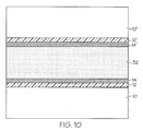
- the germanium continues to diffuse, through solid-state diffusion, from the solid 32 into the gold layers 20, 20' until equilibrium is reached and both the solid 32 and the gold layers 20, 20' all have the same composition (shown as solid 32 in Fig. 9).
- the bonding and solid state diffusion can be carried out at different temperatures.
- the bonding may take place at, for example, 450°C
- the solid-state diffusion shown in Figs. 8 and 9 may take place at an elevated temperature such as 500°C.
- the particular bonding and solid-state diffusion temperatures will depend upon the properties of the bonding materials 16, 16'.
- the solid 32 formed after solid state diffusion is a gold/germanium alloy or solid solution alloy that may have a composition at point C of Fig. 12 (i.e. about 3 atomic percent germanium).
- the solid solution 32 when the solid solution 32 has a composition at point C, the solid solution 32 has an atomic percentage of about 3 atomic percent germanium and a melting temperature of 450°C. However, the amount of available germanium may be restricted such that the resultant solid 32 has a composition of less than 3 atomic percent germanium (e.g., as low as about 0.5 atomic percent germanium or even lower). With reference to the phase diagram of Fig. 12, reducing the atomic percentage of germanium to lower than 3 atomic percent provides a solution located on the solidus line 39 above and to the left of point C. Moving the composition to the left of point C provides a solid solution 32 with a melting point above 450°C, up to a theoretical maximum of 1064°C.
- the initial thicknesses of the gold 20, 20' and germanium layers 18, 18' determine the end composition of the solid solution 32.
- the initial germanium layers 18, 18' i.e. of Fig. 3 each have a thickness of about 300 Angstroms
- the initial gold layers 20, 20' each have a thickness of about 30,000 Angstroms (with, in this example, no or negligible gold being provided by the capping layers 17, 17').
- the relative thicknesses of the gold and germanium layers can be selected and controlled to ensure that the resultant solid solution 32 has the desired amount of germanium (i.e., in this example about 1 atomic percent) upon complete diffusion of the germanium in the gold.
- the initial germanium layers 18, 18' each have a thickness of about 150 Angstroms and the initial gold layers 20, 20' each have a thickness of about 30,000 Angstroms (again, with no or negligible gold being provided by the capping layers 17, 17').
- the end bond or solid solution material 32 has 0.5 atomic percent germanium.
- the germanium layers 18, 18' should have a sufficient thickness to form an initial liquid surface of sufficient volume to ensure the germanium/gold layers 18, 18'/20, 20' flow together in the liquid state and fill any gaps to provide a complete bond.
- the relative thicknesses for these other materials would be adjusted based upon their material properties and their phase diagram to provide the desired composition for the end bond material.
- a germanium-scavenging material may be provided and located in the second bonding material 20, 20'. At a sufficient temperature, the germanium-scavenging material will react with the germanium 18, 18' when the germanium diffuses in the solid solution. The germanium-scavenging material and germanium will react to create finely dispersed intermetallic compounds. In this manner the germanium scavenging material reduces the concentration of germanium, thereby raising the melting point of the solid solution 32 while not adversely affecting the strength of the resultant bond 32.
- the germanium-scavenging material can be a variety of materials, including but not limited to platinum, nickel and chromium. Of course, the scavenging materials will be made of various other compositions when the material to be scavenged is a material other than germanium (i.e. when tin or silicon are utilized in place of germanium).
- the scavenging material may take the form of a discrete layer located between the second bonding layer 20 and anti-diffusion layer 14. Alternately, the scavenging material may be co-sputtered with the second bonding layer 20 (i.e. deposited at the same time as the second bonding layer to form numerous discrete layers or a gradient within the second bonding layer 20).
- the germanium scavenging material is preferably concentrated on the outer edges of the second bonding layer 20 (i.e. the edges of the second bonding layer 20 facing the anti-diffusion layer 14) so that germanium diffusing outwardly in the solid state is scavenged.
- the scavenging material may also be a part or component of the adhesion layer 12 and/or anti-diffusion layer 14, or integrated into the adhesion layer 12 and/or anti-diffusion layer 14.
- the anti-diffusion layer 14 is platinum
- that anti-diffusion layer 14 may also function as a germanium scavenging material.
- the germanium scavenging material may be added to the adhesion layer 12 and/or anti-diffusion layer 14 as a separate material.
- germanium-scavenging material allows some latitude in the strict thickness controls and allows for greater flexibility in the manufacturing process. In particular, it can be difficult and expensive to strictly control the thickness of the germanium layers 18, 18' and gold layers 20, 20'. For example, it can be difficult to limit the thickness of the initial germanium layers 18, 18' to 300 Angstroms, and the thickness of the initial gold layers 20, 20' to 30,000 Angstroms as in the example outlined above.
- the use of a germanium-scavenging material allows for some variance in the thickness controls, as extra germanium can be scavenged away.
- the transient liquid phase bonding method described above preferably takes place at a temperature less than about 600°C, or further preferably less than about 500°C. Due to the relatively low eutectic temperature of gold/germanium eutectic 32 (as well as various other eutectic alloys), this bonding method can be utilized to bond components having relatively temperature-sensitive materials (i.e., such as aluminum bond pads, which have a melting point of about 660°C) without damaging or melting such temperature-sensitive materials. The resultant bond has a melting temperature preferably greater than about 600°C, or more preferably greater than about 800°C, or most preferably greater than about 1000°C.
- the transient liquid joining process of the present invention allows the joining of two materials at a relatively low temperature and results in a bond having a relatively high melting temperature.
- the difference between the bonding temperature and the melting temperature of the resultant alloy is preferably at least about 400°C, or further preferably at least about 500°C, or most preferably at least about 640°C.
- Figs. 2 and 3 illustrate each of the substrates 10, 10' as having a layer of gold 20 and germanium 18 located thereon.
- the substrates 10, 10' may include only gold or only germanium.
- the relative thicknesses of the gold and germanium should be adjusted to provide for the desired composition of the resultant solid solution composition.
- gold/silicon or gold/tin eutectic combinations may be utilized as the materials of the bonding layers 16, 16'. This bonding method can be used in bonding complete wafer surfaces (as shown in Figs. 1-10) in a manner similar to glass frit bonding or oxide bonding.
- Each wafer or substrate 10 can be coated with the bonding layers 16, and heat can be applied under load until the heated bonding layers 16 merge and solidify.
- the materials of the bonding layers 16 are preferably metallic, the resultant bond is electrically conductive which allows bonding to electronic elements such as bond pads, contacts, bond wires, etc.
- Fig. 11 illustrates a pair of substrates 38, 38', with each substrate 38, 38' having a pair of bonding contacts 34 located thereon.
- Each bonding contact 34 includes an adhesion layer 12, a diffusion barrier 14 and a bonding layer 16.
- the bonding contacts 34 of the substrates 38, 38' have complementary sizes and shapes. In particular, the bonding contacts 34 are arranged such that when the substrate 38' is aligned with and located on top of the substrate 38, each of the bonding contacts 34 engage each other in the manner of a standard flip chip bonding process.
- each bonding contact 34 engages and contact each other, the bonding layers 16 of each bonding contact 34 are then heated to initiate the transient liquid phase bonding outlined above, resulting in a solid solution 32 at each bonding contact 34 joining the substrates 38, 38' together.
- each of the materials of the bonding contacts 34 are preferably electrically conductive, besides providing structural joining the bonding contacts 34 also allow for electrical interconnection between the substrates 38, 38'.
- Each substrate 38, 38' may have a plurality of microstructures (not shown) located thereon, and the substrates 38, 38' may be joined as part of a batch fabrication process. After the substrates 38, 38' are joined, the joined substrates can be separated from each other, for example, by dicing through the thickness of the joined substrates 38, 38' to thereby singulate each microstructures from any other adjacent microstructures.
- the spacing or gaps between the substrates 38, 38' can be controlled by locating spacers or standoffs 36 (made of, for example, silicon oxide or other material that does not melt at the bonding temperatures) between the two substrates 38, 38'.
- spacers or standoffs 36 made of, for example, silicon oxide or other material that does not melt at the bonding temperatures
- the substrate 38 may include a plurality of containment wells 40 formed therein and located adjacent to the bonding contacts 34.
- the containment wells 40 are shaped and located such that any liquid run-off from the bonding contacts 34 (i.e. liquefied bonding materials 16) during the bonding process flow into the containment wells 40 to contain the run-off. If the liquid run-off were to spread, the run-off could react with or form solutions with the material of the substrate 38, with other bonding contacts 34, or with various other components located on the substrate 38.
- the containment wells 40 are preferably lined with a dielectric material (such as silicon dioxide) that is resistant to reacting with or forming solutions with the liquid run-off.
- the use of germanium, tin, or silicon in combination with gold provides a relatively robust bond which has a high melting point.
- the bonding method of the present invention can be used for conventional chip and wafer bonding, as well as any application which is desired to join two components together.
- the present invention allows joining at relatively low temperatures without the use of solder, fluxes or braze materials, and can be particularly useful where the bonded regions are inaccessible for adding solder or braze materials.
- the bonding method of the present invention does not require ultrasonic scrubbing in high heat which is required for conventional eutectic die bonding and may be damaging to the substrates.
Landscapes
- Pressure Welding/Diffusion-Bonding (AREA)
Applications Claiming Priority (1)
| Application Number | Priority Date | Filing Date | Title |
|---|---|---|---|
| US11/120,879 US7628309B1 (en) | 2005-05-03 | 2005-05-03 | Transient liquid phase eutectic bonding |
Publications (2)
| Publication Number | Publication Date |
|---|---|
| EP1720204A1 true EP1720204A1 (de) | 2006-11-08 |
| EP1720204B1 EP1720204B1 (de) | 2019-06-05 |
Family
ID=36870299
Family Applications (1)
| Application Number | Title | Priority Date | Filing Date |
|---|---|---|---|
| EP06112160.4A Expired - Lifetime EP1720204B1 (de) | 2005-05-03 | 2006-04-03 | Eutektische Bindung mit vorübergehender flüssiger Phase |
Country Status (2)
| Country | Link |
|---|---|
| US (2) | US7628309B1 (de) |
| EP (1) | EP1720204B1 (de) |
Cited By (7)
| Publication number | Priority date | Publication date | Assignee | Title |
|---|---|---|---|---|
| WO2011057850A3 (de) * | 2009-11-13 | 2011-07-07 | Robert Bosch Gmbh | Mikromechanisches verfahren und entsprechende anordnung zum bonden von halbleitersubstraten sowie entsprechender gebondeter halbleiterchip |
| WO2011071685A3 (en) * | 2009-12-08 | 2011-09-09 | Freescale Semiconductor, Inc. | Micro electromechanical systems (mems) having a gap stop and method therefor |
| EP2800130A1 (de) * | 2013-04-29 | 2014-11-05 | ABB Technology AG | Verbindung eines Chips mit einem Substrat durch vorübergehende flüssige Phase unter Verwendung von einem Abstandhalter |
| CN104465428A (zh) * | 2013-09-16 | 2015-03-25 | 中国科学院上海微系统与信息技术研究所 | 一种铜-铜金属热压键合的方法 |
| EP2884526A4 (de) * | 2012-08-08 | 2015-12-30 | Panasonic Ip Man Co Ltd | Montageverfahren |
| CN109153095A (zh) * | 2016-03-31 | 2019-01-04 | 泰克尼控股有限公司 | 用于在二元体系中形成接头的方法及其接头 |
| WO2020139436A1 (en) * | 2018-12-27 | 2020-07-02 | Raytheon Company | Method of filling grooves and holes in a substrate |
Families Citing this family (45)
| Publication number | Priority date | Publication date | Assignee | Title |
|---|---|---|---|---|
| US7846815B2 (en) * | 2009-03-30 | 2010-12-07 | Freescale Semiconductor, Inc. | Eutectic flow containment in a semiconductor fabrication process |
| WO2011099934A1 (en) * | 2010-02-10 | 2011-08-18 | Agency For Science, Technology And Research | A method of forming a bonded structure |
| US8905293B2 (en) * | 2010-12-09 | 2014-12-09 | Taiwan Semiconductor Manufacturing Company, Ltd. | Self-removal anti-stiction coating for bonding process |
| US9166364B2 (en) * | 2011-02-14 | 2015-10-20 | Spectrasensors, Inc. | Semiconductor laser mounting with intact diffusion barrier layer |
| US8431445B2 (en) | 2011-06-01 | 2013-04-30 | Toyota Motor Engineering & Manufacturing North America, Inc. | Multi-component power structures and methods for forming the same |
| US8803001B2 (en) | 2011-06-21 | 2014-08-12 | Toyota Motor Engineering & Manufacturing North America, Inc. | Bonding area design for transient liquid phase bonding process |
| US8573469B2 (en) | 2011-11-18 | 2013-11-05 | LuxVue Technology Corporation | Method of forming a micro LED structure and array of micro LED structures with an electrically insulating layer |
| US8794501B2 (en) | 2011-11-18 | 2014-08-05 | LuxVue Technology Corporation | Method of transferring a light emitting diode |
| US8333860B1 (en) | 2011-11-18 | 2012-12-18 | LuxVue Technology Corporation | Method of transferring a micro device |
| US8349116B1 (en) | 2011-11-18 | 2013-01-08 | LuxVue Technology Corporation | Micro device transfer head heater assembly and method of transferring a micro device |
| US8518204B2 (en) * | 2011-11-18 | 2013-08-27 | LuxVue Technology Corporation | Method of fabricating and transferring a micro device and an array of micro devices utilizing an intermediate electrically conductive bonding layer |
| US9773750B2 (en) | 2012-02-09 | 2017-09-26 | Apple Inc. | Method of transferring and bonding an array of micro devices |
| US9044822B2 (en) | 2012-04-17 | 2015-06-02 | Toyota Motor Engineering & Manufacturing North America, Inc. | Transient liquid phase bonding process for double sided power modules |
| US10058951B2 (en) | 2012-04-17 | 2018-08-28 | Toyota Motor Engineering & Manufacturing North America, Inc. | Alloy formation control of transient liquid phase bonding |
| US8814030B2 (en) * | 2012-04-17 | 2014-08-26 | Toyota Motor Engineering & Manufacturing North America, Inc. | Improvements of long term bondline reliability of power electronics operating at high temperatures |
| US9548332B2 (en) | 2012-04-27 | 2017-01-17 | Apple Inc. | Method of forming a micro LED device with self-aligned metallization stack |
| US9162880B2 (en) | 2012-09-07 | 2015-10-20 | LuxVue Technology Corporation | Mass transfer tool |
| CN105683872B (zh) | 2013-06-12 | 2020-05-12 | 罗茵尼公司 | 安置有光产生源的键盘背后照明 |
| US9296111B2 (en) | 2013-07-22 | 2016-03-29 | LuxVue Technology Corporation | Micro pick up array alignment encoder |
| US9087764B2 (en) | 2013-07-26 | 2015-07-21 | LuxVue Technology Corporation | Adhesive wafer bonding with controlled thickness variation |
| US20150048509A1 (en) * | 2013-08-16 | 2015-02-19 | Globalfoundries Singapore Pte. Ltd. | Cmos compatible wafer bonding layer and process |
| US9153548B2 (en) | 2013-09-16 | 2015-10-06 | Lux Vue Technology Corporation | Adhesive wafer bonding with sacrificial spacers for controlled thickness variation |
| US9367094B2 (en) | 2013-12-17 | 2016-06-14 | Apple Inc. | Display module and system applications |
| US9768345B2 (en) | 2013-12-20 | 2017-09-19 | Apple Inc. | LED with current injection confinement trench |
| US9583466B2 (en) | 2013-12-27 | 2017-02-28 | Apple Inc. | Etch removal of current distribution layer for LED current confinement |
| US9450147B2 (en) | 2013-12-27 | 2016-09-20 | Apple Inc. | LED with internally confined current injection area |
| US9542638B2 (en) | 2014-02-18 | 2017-01-10 | Apple Inc. | RFID tag and micro chip integration design |
| US9583533B2 (en) | 2014-03-13 | 2017-02-28 | Apple Inc. | LED device with embedded nanowire LEDs |
| US9522468B2 (en) | 2014-05-08 | 2016-12-20 | Apple Inc. | Mass transfer tool manipulator assembly with remote center of compliance |
| US9318475B2 (en) | 2014-05-15 | 2016-04-19 | LuxVue Technology Corporation | Flexible display and method of formation with sacrificial release layer |
| US9741286B2 (en) | 2014-06-03 | 2017-08-22 | Apple Inc. | Interactive display panel with emitting and sensing diodes |
| US9624100B2 (en) | 2014-06-12 | 2017-04-18 | Apple Inc. | Micro pick up array pivot mount with integrated strain sensing elements |
| US9425151B2 (en) | 2014-06-17 | 2016-08-23 | Apple Inc. | Compliant electrostatic transfer head with spring support layer |
| US9570002B2 (en) | 2014-06-17 | 2017-02-14 | Apple Inc. | Interactive display panel with IR diodes |
| US10568213B2 (en) | 2014-07-31 | 2020-02-18 | Skyworks Solutions, Inc. | Multilayered transient liquid phase bonding |
| US10541152B2 (en) | 2014-07-31 | 2020-01-21 | Skyworks Solutions, Inc. | Transient liquid phase material bonding and sealing structures and methods of forming same |
| US9705432B2 (en) | 2014-09-30 | 2017-07-11 | Apple Inc. | Micro pick up array pivot mount design for strain amplification |
| US9828244B2 (en) | 2014-09-30 | 2017-11-28 | Apple Inc. | Compliant electrostatic transfer head with defined cavity |
| US9478583B2 (en) | 2014-12-08 | 2016-10-25 | Apple Inc. | Wearable display having an array of LEDs on a conformable silicon substrate |
| WO2017100256A1 (en) * | 2015-12-08 | 2017-06-15 | Skyworks Solutions, Inc. | Transient liquid phase material bonding and sealing structures and methods of forming same |
| KR102298484B1 (ko) | 2016-01-15 | 2021-09-03 | 로히니, 엘엘씨. | 장치 상의 커버를 통해 후면 발광하는 장치 및 방법 |
| US11000915B2 (en) * | 2016-03-31 | 2021-05-11 | Texas Instruments Incorporated | Stabilized transient liquid phase metal bonding material for hermetic wafer level packaging of MEMS devices |
| US10439587B2 (en) | 2016-12-02 | 2019-10-08 | Skyworks Solutions, Inc. | Methods of manufacturing electronic devices formed in a cavity |
| CN111223766B (zh) * | 2018-11-23 | 2022-07-05 | 上海新微技术研发中心有限公司 | 共晶键合的方法 |
| ES2928498T3 (es) * | 2019-05-07 | 2022-11-18 | Light Med Usa Inc | Método de fase líquida transitoria de plata-indio de unión de dispositivo semiconductor y soporte de dispersión de calor y estructura semiconductora que tiene una junta de unión de fase líquida transitoria de plata-indio |
Citations (4)
| Publication number | Priority date | Publication date | Assignee | Title |
|---|---|---|---|---|
| US3200490A (en) | 1962-12-07 | 1965-08-17 | Philco Corp | Method of forming ohmic bonds to a germanium-coated silicon body with eutectic alloyforming materials |
| EP0119691A2 (de) | 1983-03-15 | 1984-09-26 | Stc Plc | Verbinden von Halbleiterkörpern |
| GB2221570A (en) | 1988-08-04 | 1990-02-07 | Stc Plc | Bonding a semiconductor to a heat sink |
| EP0585084A1 (de) | 1992-08-28 | 1994-03-02 | AT&T Corp. | Verfahren für eine permanente metallische Verbindung |
Family Cites Families (85)
| Publication number | Priority date | Publication date | Assignee | Title |
|---|---|---|---|---|
| US3396454A (en) * | 1964-01-23 | 1968-08-13 | Allis Chalmers Mfg Co | Method of forming ohmic contacts in semiconductor devices |
| US3619742A (en) | 1970-05-21 | 1971-11-09 | Rosemount Eng Co Ltd | Shielded capacitance pressure sensor |
| US3879746A (en) | 1972-05-30 | 1975-04-22 | Bell Telephone Labor Inc | Gate metallization structure |
| FR2217290B1 (de) * | 1972-12-01 | 1975-03-28 | Quartex Sa | |
| US3877063A (en) * | 1973-06-27 | 1975-04-08 | Hewlett Packard Co | Metallization structure and process for semiconductor devices |
| US3935986A (en) | 1975-03-03 | 1976-02-03 | Texas Instruments Incorporated | Solid state bonding process employing the isothermal solidification of a liquid interface |
| US3994430A (en) * | 1975-07-30 | 1976-11-30 | General Electric Company | Direct bonding of metals to ceramics and metals |
| US4141456A (en) * | 1976-08-30 | 1979-02-27 | Rca Corp. | Apparatus and method for aligning wafers |
| US4215156A (en) | 1977-08-26 | 1980-07-29 | International Business Machines Corporation | Method for fabricating tantalum semiconductor contacts |
| US4233337A (en) | 1978-05-01 | 1980-11-11 | International Business Machines Corporation | Method for forming semiconductor contacts |
| US4330343A (en) | 1979-01-04 | 1982-05-18 | The United States Of America As Represented By The Secretary Of The Navy | Refractory passivated ion-implanted GaAs ohmic contacts |
| CA1138795A (en) | 1980-02-19 | 1983-01-04 | Goodrich (B.F.) Company (The) | Escape slide and life raft |
| US5536967A (en) | 1980-12-30 | 1996-07-16 | Fujitsu Limited | Semiconductor device including Schottky gate of silicide and method for the manufacture of the same |
| US5200349A (en) | 1980-12-30 | 1993-04-06 | Fujitsu Limited | Semiconductor device including schotky gate of silicide and method for the manufacture of the same |
| US4400869A (en) | 1981-02-12 | 1983-08-30 | Becton Dickinson And Company | Process for producing high temperature pressure transducers and semiconductors |
| DE3304588A1 (de) | 1983-02-10 | 1984-08-16 | Siemens AG, 1000 Berlin und 8000 München | Verfahren zum herstellen von mos-transistoren mit flachen source/drain-gebieten, kurzen kanallaengen und einer selbstjustierten, aus einem metallsilizid bestehenden kontaktierungsebene |
| DE3326142A1 (de) | 1983-07-20 | 1985-01-31 | Siemens AG, 1000 Berlin und 8000 München | Integrierte halbleiterschaltung mit einer aus aluminium oder aus einer aluminiumlegierung bestehenden aeusseren kontaktleiterbahnebene |
| US4702941A (en) * | 1984-03-27 | 1987-10-27 | Motorola Inc. | Gold metallization process |
| US4637129A (en) | 1984-07-30 | 1987-01-20 | At&T Bell Laboratories | Selective area III-V growth and lift-off using tungsten patterning |
| DE3440568A1 (de) | 1984-11-07 | 1986-05-15 | Robert Bosch Gmbh, 7000 Stuttgart | Hochdrucksensor |
| US4777826A (en) | 1985-06-20 | 1988-10-18 | Rosemount Inc. | Twin film strain gauge system |
| JPS61296764A (ja) | 1985-06-25 | 1986-12-27 | Mitsubishi Electric Corp | 金属電極配線膜を有する半導体装置 |
| US4758534A (en) | 1985-11-13 | 1988-07-19 | Bell Communications Research, Inc. | Process for producing porous refractory metal layers embedded in semiconductor devices |
| US4960718A (en) | 1985-12-13 | 1990-10-02 | Allied-Signal Inc. | MESFET device having a semiconductor surface barrier layer |
| US5038996A (en) * | 1988-10-12 | 1991-08-13 | International Business Machines Corporation | Bonding of metallic surfaces |
| US4939497A (en) | 1989-04-18 | 1990-07-03 | Nippon Soken, Inc. | Pressure sensor |
| US5181417A (en) | 1989-07-10 | 1993-01-26 | Nippon Soken, Inc. | Pressure detecting device |
| US5095759A (en) * | 1990-06-01 | 1992-03-17 | Gte Products Corporation | Platinum electrode bonded to ceramic |
| JPH04268725A (ja) | 1991-02-25 | 1992-09-24 | Canon Inc | 力学量検出センサおよびその製造方法 |
| US5182218A (en) | 1991-02-25 | 1993-01-26 | Sumitomo Electric Industries, Ltd. | Production methods for compound semiconductor device having lightly doped drain structure |
| FR2681472B1 (fr) | 1991-09-18 | 1993-10-29 | Commissariat Energie Atomique | Procede de fabrication de films minces de materiau semiconducteur. |
| US5257547A (en) * | 1991-11-26 | 1993-11-02 | Honeywell Inc. | Amplified pressure transducer |
| JPH05200539A (ja) * | 1992-01-24 | 1993-08-10 | Honda Motor Co Ltd | 半導体基板接合方法 |
| JP2796919B2 (ja) | 1992-05-11 | 1998-09-10 | インターナショナル・ビジネス・マシーンズ・コーポレーション | メタライゼーション複合体および半導体デバイス |
| US5286676A (en) | 1992-06-15 | 1994-02-15 | Hewlett-Packard Company | Methods of making integrated circuit barrier structures |
| JPH06132545A (ja) | 1992-10-19 | 1994-05-13 | Mitsubishi Electric Corp | 圧力検出装置 |
| US5346855A (en) | 1993-01-19 | 1994-09-13 | At&T Bell Laboratories | Method of making an INP-based DFB laser |
| US5286671A (en) | 1993-05-07 | 1994-02-15 | Kulite Semiconductor Products, Inc. | Fusion bonding technique for use in fabricating semiconductor devices |
| US5369300A (en) | 1993-06-10 | 1994-11-29 | Delco Electronics Corporation | Multilayer metallization for silicon semiconductor devices including a diffusion barrier formed of amorphous tungsten/silicon |
| US5559817A (en) | 1994-11-23 | 1996-09-24 | Lucent Technologies Inc. | Complaint layer metallization |
| US5561083A (en) | 1994-12-29 | 1996-10-01 | Lucent Technologies Inc. | Method of making multilayered Al-alloy structure for metal conductors |
| JPH08264562A (ja) | 1995-03-24 | 1996-10-11 | Mitsubishi Electric Corp | 半導体装置,及びその製造方法 |
| EP0735353B2 (de) | 1995-03-31 | 2004-03-17 | Endress + Hauser Gmbh + Co. | Drucksensor |
| DE69629024T2 (de) | 1995-04-28 | 2004-04-22 | Rosemount Inc., Eden Prairie | Druckwandler mit montageanordnung mit hochdruckisolator |
| US5600071A (en) | 1995-09-05 | 1997-02-04 | Motorola, Inc. | Vertically integrated sensor structure and method |
| US5637905A (en) | 1996-02-01 | 1997-06-10 | New Jersey Institute Of Technology | High temperature, pressure and displacement microsensor |
| US5882532A (en) | 1996-05-31 | 1999-03-16 | Hewlett-Packard Company | Fabrication of single-crystal silicon structures using sacrificial-layer wafer bonding |
| US6027957A (en) | 1996-06-27 | 2000-02-22 | University Of Maryland | Controlled solder interdiffusion for high power semiconductor laser diode die bonding |
| US5802091A (en) | 1996-11-27 | 1998-09-01 | Lucent Technologies Inc. | Tantalum-aluminum oxide coatings for semiconductor devices |
| US6191007B1 (en) | 1997-04-28 | 2001-02-20 | Denso Corporation | Method for manufacturing a semiconductor substrate |
| US5935430A (en) * | 1997-04-30 | 1999-08-10 | Hewlett-Packard Company | Structure for capturing express transient liquid phase during diffusion bonding of planar devices |
| JPH1164137A (ja) | 1997-08-25 | 1999-03-05 | Hitachi Ltd | 半導体圧力センサ |
| JPH1179872A (ja) | 1997-09-03 | 1999-03-23 | Sumitomo Electric Ind Ltd | メタライズ窒化ケイ素系セラミックス、その製造方法及びその製造に用いるメタライズ組成物 |
| ATE294373T1 (de) | 1997-09-11 | 2005-05-15 | Honeywell Inc | Feststoff-flüssigkeits-interdiffusionsverbindun für ringlaserkreisel |
| US5955771A (en) | 1997-11-12 | 1999-09-21 | Kulite Semiconductor Products, Inc. | Sensors for use in high vibrational applications and methods for fabricating same |
| US5882738A (en) | 1997-12-19 | 1999-03-16 | Advanced Micro Devices, Inc. | Apparatus and method to improve electromigration performance by use of amorphous barrier layer |
| US6465271B1 (en) | 1998-07-07 | 2002-10-15 | Wen H. Ko | Method of fabricating silicon capacitive sensor |
| US6058782A (en) | 1998-09-25 | 2000-05-09 | Kulite Semiconductor Products | Hermetically sealed ultra high temperature silicon carbide pressure transducers and method for fabricating same |
| US6351996B1 (en) * | 1998-11-12 | 2002-03-05 | Maxim Integrated Products, Inc. | Hermetic packaging for semiconductor pressure sensors |
| FR2786564B1 (fr) | 1998-11-27 | 2001-04-13 | Commissariat Energie Atomique | Capteur de pression a membrane comportant du carbure de silicium et procede de fabrication |
| US6363792B1 (en) | 1999-01-29 | 2002-04-02 | Kulite Semiconductor Products, Inc. | Ultra high temperature transducer structure |
| US6320265B1 (en) | 1999-04-12 | 2001-11-20 | Lucent Technologies Inc. | Semiconductor device with high-temperature ohmic contact and method of forming the same |
| JP3619065B2 (ja) * | 1999-07-16 | 2005-02-09 | 株式会社山武 | 圧力センサ |
| US6932951B1 (en) | 1999-10-29 | 2005-08-23 | Massachusetts Institute Of Technology | Microfabricated chemical reactor |
| US6272928B1 (en) | 2000-01-24 | 2001-08-14 | Kulite Semiconductor Products | Hermetically sealed absolute and differential pressure transducer |
| JP3706903B2 (ja) | 2000-08-10 | 2005-10-19 | 独立行政法人産業技術総合研究所 | フレキシブル高感度セラミックスセンサー |
| DE10060439A1 (de) | 2000-12-05 | 2002-06-13 | Osram Opto Semiconductors Gmbh | Kontaktmetallisierung für GaN-basierende Halbleiterstrukturen und Verfahren zu deren Herstellung |
| US6956268B2 (en) | 2001-05-18 | 2005-10-18 | Reveo, Inc. | MEMS and method of manufacturing MEMS |
| US6550665B1 (en) * | 2001-06-06 | 2003-04-22 | Indigo Systems Corporation | Method for electrically interconnecting large contact arrays using eutectic alloy bumping |
| JP2002368168A (ja) | 2001-06-13 | 2002-12-20 | Hitachi Ltd | 半導体装置用複合部材、それを用いた絶縁型半導体装置、又は非絶縁型半導体装置 |
| US6566158B2 (en) | 2001-08-17 | 2003-05-20 | Rosemount Aerospace Inc. | Method of preparing a semiconductor using ion implantation in a SiC layer |
| US7081271B2 (en) | 2001-12-07 | 2006-07-25 | Applied Materials, Inc. | Cyclical deposition of refractory metal silicon nitride |
| US6564644B1 (en) | 2001-12-21 | 2003-05-20 | Kulite Semiconductor Products, Inc. | High temperature surface mount transducer |
| US6595066B1 (en) | 2002-04-05 | 2003-07-22 | Kulite Semiconductor Products, Inc. | Stopped leadless differential sensor |
| US6706549B1 (en) | 2002-04-12 | 2004-03-16 | The United States Of America As Represented By The Administrator Of The National Aeronautics And Space Administration | Multi-functional micro electromechanical devices and method of bulk manufacturing same |
| US6586330B1 (en) | 2002-05-07 | 2003-07-01 | Tokyo Electron Limited | Method for depositing conformal nitrified tantalum silicide films by thermal CVD |
| US6612178B1 (en) | 2002-05-13 | 2003-09-02 | Kulite Semiconductor Products, Inc. | Leadless metal media protected pressure sensor |
| JP4240445B2 (ja) | 2002-05-31 | 2009-03-18 | 独立行政法人産業技術総合研究所 | 超高配向窒化アルミニウム薄膜を用いた圧電素子とその製造方法 |
| WO2004031711A1 (ja) | 2002-10-01 | 2004-04-15 | National Institute Of Advanced Industrial Science And Technology | 圧電センサおよびそれを備えた入力装置 |
| US6845664B1 (en) | 2002-10-03 | 2005-01-25 | The United States Of America As Represented By The Administrator Of National Aeronautics And Space Administration | MEMS direct chip attach packaging methodologies and apparatuses for harsh environments |
| US6943097B2 (en) | 2003-08-19 | 2005-09-13 | International Business Machines Corporation | Atomic layer deposition of metallic contacts, gates and diffusion barriers |
| US7410833B2 (en) * | 2004-03-31 | 2008-08-12 | International Business Machines Corporation | Interconnections for flip-chip using lead-free solders and having reaction barrier layers |
| US7107853B2 (en) * | 2004-04-23 | 2006-09-19 | Kulite Semiconductor Products, Inc. | Pressure transducer for measuring low dynamic pressures in the presence of high static pressures |
| US7261793B2 (en) | 2004-08-13 | 2007-08-28 | Hewlett-Packard Development Company, L.P. | System and method for low temperature plasma-enhanced bonding |
| US6928878B1 (en) | 2004-09-28 | 2005-08-16 | Rosemount Aerospace Inc. | Pressure sensor |
-
2005
- 2005-05-03 US US11/120,879 patent/US7628309B1/en active Active
-
2006
- 2006-04-03 EP EP06112160.4A patent/EP1720204B1/de not_active Expired - Lifetime
-
2009
- 2009-10-28 US US12/607,456 patent/US20100047491A1/en not_active Abandoned
Patent Citations (4)
| Publication number | Priority date | Publication date | Assignee | Title |
|---|---|---|---|---|
| US3200490A (en) | 1962-12-07 | 1965-08-17 | Philco Corp | Method of forming ohmic bonds to a germanium-coated silicon body with eutectic alloyforming materials |
| EP0119691A2 (de) | 1983-03-15 | 1984-09-26 | Stc Plc | Verbinden von Halbleiterkörpern |
| GB2221570A (en) | 1988-08-04 | 1990-02-07 | Stc Plc | Bonding a semiconductor to a heat sink |
| EP0585084A1 (de) | 1992-08-28 | 1994-03-02 | AT&T Corp. | Verfahren für eine permanente metallische Verbindung |
Cited By (14)
| Publication number | Priority date | Publication date | Assignee | Title |
|---|---|---|---|---|
| US8638000B2 (en) | 2009-11-13 | 2014-01-28 | Robert Bosch Gmbh | Micromechanical method and corresponding assembly for bonding semiconductor substrates and correspondingly bonded semiconductor chip |
| WO2011057850A3 (de) * | 2009-11-13 | 2011-07-07 | Robert Bosch Gmbh | Mikromechanisches verfahren und entsprechende anordnung zum bonden von halbleitersubstraten sowie entsprechender gebondeter halbleiterchip |
| WO2011071685A3 (en) * | 2009-12-08 | 2011-09-09 | Freescale Semiconductor, Inc. | Micro electromechanical systems (mems) having a gap stop and method therefor |
| US8119431B2 (en) | 2009-12-08 | 2012-02-21 | Freescale Semiconductor, Inc. | Method of forming a micro-electromechanical system (MEMS) having a gap stop |
| CN102762490A (zh) * | 2009-12-08 | 2012-10-31 | 飞思卡尔半导体公司 | 具有间隙挡块的微机电系统(mems)及其制造方法 |
| CN102762490B (zh) * | 2009-12-08 | 2015-09-23 | 飞思卡尔半导体公司 | 具有间隙挡块的微机电系统(mems)及其制造方法 |
| EP2884526A4 (de) * | 2012-08-08 | 2015-12-30 | Panasonic Ip Man Co Ltd | Montageverfahren |
| EP2800130A1 (de) * | 2013-04-29 | 2014-11-05 | ABB Technology AG | Verbindung eines Chips mit einem Substrat durch vorübergehende flüssige Phase unter Verwendung von einem Abstandhalter |
| CN104465428A (zh) * | 2013-09-16 | 2015-03-25 | 中国科学院上海微系统与信息技术研究所 | 一种铜-铜金属热压键合的方法 |
| CN104465428B (zh) * | 2013-09-16 | 2017-10-13 | 中国科学院上海微系统与信息技术研究所 | 一种铜‑铜金属热压键合的方法 |
| CN109153095A (zh) * | 2016-03-31 | 2019-01-04 | 泰克尼控股有限公司 | 用于在二元体系中形成接头的方法及其接头 |
| US11141810B2 (en) | 2016-03-31 | 2021-10-12 | Techni Holding As | Non-eutectic bonding |
| WO2020139436A1 (en) * | 2018-12-27 | 2020-07-02 | Raytheon Company | Method of filling grooves and holes in a substrate |
| US11101130B2 (en) | 2018-12-27 | 2021-08-24 | Raytheon Company | Method of filling grooves and holes in a substrate |
Also Published As
| Publication number | Publication date |
|---|---|
| EP1720204B1 (de) | 2019-06-05 |
| US7628309B1 (en) | 2009-12-08 |
| US20100047491A1 (en) | 2010-02-25 |
Similar Documents
| Publication | Publication Date | Title |
|---|---|---|
| EP1720204B1 (de) | Eutektische Bindung mit vorübergehender flüssiger Phase | |
| EP1722004B1 (de) | Substrat mit einer Metallisierungshaftschicht | |
| US8293582B2 (en) | Method of substrate bonding with bonding material having rare Earth metal | |
| US7065867B2 (en) | Low temperature hermetic sealing method having passivation layer | |
| Xu et al. | Wafer-level SLID bonding for MEMS encapsulation | |
| US20040266048A1 (en) | Bonding for a micro-electro-mechanical system (MEMS) and MEMS based devices | |
| US8957522B2 (en) | Semiconductor device and manufacturing method of semiconductor device | |
| US9181088B2 (en) | Objects assembly through a sealing bead including intermetallic compounds | |
| JP7248774B2 (ja) | 半導体チップを基板の上に固定する方法および電子構成素子 | |
| WO2011099934A1 (en) | A method of forming a bonded structure | |
| EP2363373A1 (de) | Procédé de collage pour systèmes micro et nano sensibles | |
| CN109755208A (zh) | 一种接合材料、半导体装置及其制造方法 | |
| JP2003017375A (ja) | セレン化反応を利用する基板ボンディング法 | |
| JP5243962B2 (ja) | カバーウエハー又は構造要素−カバー、ウエハー構造部分又はマイクロ技術に使用可能な構造要素、及び対応するウエハー−部分又は構造要素−部分をはんだ付けする方法 | |
| US5106009A (en) | Methods of joining components | |
| US7851910B2 (en) | Diffusion soldered semiconductor device | |
| EP0880801B1 (de) | BEFESTIGTER SiC-WÜRFEL UND VERFAHREN ZUR BEFESTIGUNG VON SiC-WÜRFELN | |
| KR102315100B1 (ko) | 반도체 디바이스와 열-확산 마운트를 결합하기 위한 은-인듐 전이 액체상 방법 및 은-인듐 전이 액체상 결합 조인트를 가지는 반도체 구조체 | |
| JP2005032834A (ja) | 半導体チップと基板との接合方法 | |
| US20070099410A1 (en) | Hard intermetallic bonding of wafers for MEMS applications | |
| EP0186585A2 (de) | Verfahren zum Befestigen von Plättchen | |
| US10062622B2 (en) | Electrolytic seal | |
| JPH0786444A (ja) | 半導体用複合放熱基板の製造方法 | |
| JPH038346A (ja) | ろう付け材料 | |
| RU2342231C2 (ru) | Способ соединения двух твердотельных образцов |
Legal Events
| Date | Code | Title | Description |
|---|---|---|---|
| PUAI | Public reference made under article 153(3) epc to a published international application that has entered the european phase |
Free format text: ORIGINAL CODE: 0009012 |
|
| AK | Designated contracting states |
Kind code of ref document: A1 Designated state(s): AT BE BG CH CY CZ DE DK EE ES FI FR GB GR HU IE IS IT LI LT LU LV MC NL PL PT RO SE SI SK TR |
|
| AX | Request for extension of the european patent |
Extension state: AL BA HR MK YU |
|
| RIN1 | Information on inventor provided before grant (corrected) |
Inventor name: GUO, SHUWEN Inventor name: CHILDRESS, KIMIKO Inventor name: ERIKSEN, ODD HARALD STEEN |
|
| 17P | Request for examination filed |
Effective date: 20070508 |
|
| AKX | Designation fees paid |
Designated state(s): AT BE BG CH CY CZ DE DK EE ES FI FR GB GR HU IE IS IT LI LT LU LV MC NL PL PT RO SE SI SK TR |
|
| 17Q | First examination report despatched |
Effective date: 20070627 |
|
| GRAP | Despatch of communication of intention to grant a patent |
Free format text: ORIGINAL CODE: EPIDOSNIGR1 |
|
| STAA | Information on the status of an ep patent application or granted ep patent |
Free format text: STATUS: GRANT OF PATENT IS INTENDED |
|
| INTG | Intention to grant announced |
Effective date: 20181207 |
|
| GRAS | Grant fee paid |
Free format text: ORIGINAL CODE: EPIDOSNIGR3 |
|
| GRAA | (expected) grant |
Free format text: ORIGINAL CODE: 0009210 |
|
| STAA | Information on the status of an ep patent application or granted ep patent |
Free format text: STATUS: THE PATENT HAS BEEN GRANTED |
|
| AK | Designated contracting states |
Kind code of ref document: B1 Designated state(s): AT BE BG CH CY CZ DE DK EE ES FI FR GB GR HU IE IS IT LI LT LU LV MC NL PL PT RO SE SI SK TR |
|
| REG | Reference to a national code |
Ref country code: GB Ref legal event code: FG4D |
|
| REG | Reference to a national code |
Ref country code: CH Ref legal event code: EP |
|
| REG | Reference to a national code |
Ref country code: AT Ref legal event code: REF Ref document number: 1140848 Country of ref document: AT Kind code of ref document: T Effective date: 20190615 |
|
| REG | Reference to a national code |
Ref country code: DE Ref legal event code: R096 Ref document number: 602006058084 Country of ref document: DE |
|
| REG | Reference to a national code |
Ref country code: IE Ref legal event code: FG4D |
|
| REG | Reference to a national code |
Ref country code: NL Ref legal event code: MP Effective date: 20190605 |
|
| REG | Reference to a national code |
Ref country code: LT Ref legal event code: MG4D |
|
| PG25 | Lapsed in a contracting state [announced via postgrant information from national office to epo] |
Ref country code: LT Free format text: LAPSE BECAUSE OF FAILURE TO SUBMIT A TRANSLATION OF THE DESCRIPTION OR TO PAY THE FEE WITHIN THE PRESCRIBED TIME-LIMIT Effective date: 20190605 Ref country code: FI Free format text: LAPSE BECAUSE OF FAILURE TO SUBMIT A TRANSLATION OF THE DESCRIPTION OR TO PAY THE FEE WITHIN THE PRESCRIBED TIME-LIMIT Effective date: 20190605 Ref country code: ES Free format text: LAPSE BECAUSE OF FAILURE TO SUBMIT A TRANSLATION OF THE DESCRIPTION OR TO PAY THE FEE WITHIN THE PRESCRIBED TIME-LIMIT Effective date: 20190605 Ref country code: SE Free format text: LAPSE BECAUSE OF FAILURE TO SUBMIT A TRANSLATION OF THE DESCRIPTION OR TO PAY THE FEE WITHIN THE PRESCRIBED TIME-LIMIT Effective date: 20190605 |
|
| PG25 | Lapsed in a contracting state [announced via postgrant information from national office to epo] |
Ref country code: BG Free format text: LAPSE BECAUSE OF FAILURE TO SUBMIT A TRANSLATION OF THE DESCRIPTION OR TO PAY THE FEE WITHIN THE PRESCRIBED TIME-LIMIT Effective date: 20190905 Ref country code: GR Free format text: LAPSE BECAUSE OF FAILURE TO SUBMIT A TRANSLATION OF THE DESCRIPTION OR TO PAY THE FEE WITHIN THE PRESCRIBED TIME-LIMIT Effective date: 20190906 Ref country code: LV Free format text: LAPSE BECAUSE OF FAILURE TO SUBMIT A TRANSLATION OF THE DESCRIPTION OR TO PAY THE FEE WITHIN THE PRESCRIBED TIME-LIMIT Effective date: 20190605 |
|
| REG | Reference to a national code |
Ref country code: AT Ref legal event code: MK05 Ref document number: 1140848 Country of ref document: AT Kind code of ref document: T Effective date: 20190605 |
|
| PG25 | Lapsed in a contracting state [announced via postgrant information from national office to epo] |
Ref country code: EE Free format text: LAPSE BECAUSE OF FAILURE TO SUBMIT A TRANSLATION OF THE DESCRIPTION OR TO PAY THE FEE WITHIN THE PRESCRIBED TIME-LIMIT Effective date: 20190605 Ref country code: SK Free format text: LAPSE BECAUSE OF FAILURE TO SUBMIT A TRANSLATION OF THE DESCRIPTION OR TO PAY THE FEE WITHIN THE PRESCRIBED TIME-LIMIT Effective date: 20190605 Ref country code: PT Free format text: LAPSE BECAUSE OF FAILURE TO SUBMIT A TRANSLATION OF THE DESCRIPTION OR TO PAY THE FEE WITHIN THE PRESCRIBED TIME-LIMIT Effective date: 20191007 Ref country code: AT Free format text: LAPSE BECAUSE OF FAILURE TO SUBMIT A TRANSLATION OF THE DESCRIPTION OR TO PAY THE FEE WITHIN THE PRESCRIBED TIME-LIMIT Effective date: 20190605 Ref country code: CZ Free format text: LAPSE BECAUSE OF FAILURE TO SUBMIT A TRANSLATION OF THE DESCRIPTION OR TO PAY THE FEE WITHIN THE PRESCRIBED TIME-LIMIT Effective date: 20190605 Ref country code: NL Free format text: LAPSE BECAUSE OF FAILURE TO SUBMIT A TRANSLATION OF THE DESCRIPTION OR TO PAY THE FEE WITHIN THE PRESCRIBED TIME-LIMIT Effective date: 20190605 Ref country code: RO Free format text: LAPSE BECAUSE OF FAILURE TO SUBMIT A TRANSLATION OF THE DESCRIPTION OR TO PAY THE FEE WITHIN THE PRESCRIBED TIME-LIMIT Effective date: 20190605 |
|
| PG25 | Lapsed in a contracting state [announced via postgrant information from national office to epo] |
Ref country code: IT Free format text: LAPSE BECAUSE OF FAILURE TO SUBMIT A TRANSLATION OF THE DESCRIPTION OR TO PAY THE FEE WITHIN THE PRESCRIBED TIME-LIMIT Effective date: 20190605 Ref country code: IS Free format text: LAPSE BECAUSE OF FAILURE TO SUBMIT A TRANSLATION OF THE DESCRIPTION OR TO PAY THE FEE WITHIN THE PRESCRIBED TIME-LIMIT Effective date: 20191005 |
|
| REG | Reference to a national code |
Ref country code: DE Ref legal event code: R097 Ref document number: 602006058084 Country of ref document: DE |
|
| PG25 | Lapsed in a contracting state [announced via postgrant information from national office to epo] |
Ref country code: TR Free format text: LAPSE BECAUSE OF FAILURE TO SUBMIT A TRANSLATION OF THE DESCRIPTION OR TO PAY THE FEE WITHIN THE PRESCRIBED TIME-LIMIT Effective date: 20190605 |
|
| PLBE | No opposition filed within time limit |
Free format text: ORIGINAL CODE: 0009261 |
|
| STAA | Information on the status of an ep patent application or granted ep patent |
Free format text: STATUS: NO OPPOSITION FILED WITHIN TIME LIMIT |
|
| PG25 | Lapsed in a contracting state [announced via postgrant information from national office to epo] |
Ref country code: PL Free format text: LAPSE BECAUSE OF FAILURE TO SUBMIT A TRANSLATION OF THE DESCRIPTION OR TO PAY THE FEE WITHIN THE PRESCRIBED TIME-LIMIT Effective date: 20190605 Ref country code: DK Free format text: LAPSE BECAUSE OF FAILURE TO SUBMIT A TRANSLATION OF THE DESCRIPTION OR TO PAY THE FEE WITHIN THE PRESCRIBED TIME-LIMIT Effective date: 20190605 |
|
| 26N | No opposition filed |
Effective date: 20200306 |
|
| PG25 | Lapsed in a contracting state [announced via postgrant information from national office to epo] |
Ref country code: SI Free format text: LAPSE BECAUSE OF FAILURE TO SUBMIT A TRANSLATION OF THE DESCRIPTION OR TO PAY THE FEE WITHIN THE PRESCRIBED TIME-LIMIT Effective date: 20190605 |
|
| PG25 | Lapsed in a contracting state [announced via postgrant information from national office to epo] |
Ref country code: MC Free format text: LAPSE BECAUSE OF FAILURE TO SUBMIT A TRANSLATION OF THE DESCRIPTION OR TO PAY THE FEE WITHIN THE PRESCRIBED TIME-LIMIT Effective date: 20190605 |
|
| REG | Reference to a national code |
Ref country code: CH Ref legal event code: PL |
|
| PG25 | Lapsed in a contracting state [announced via postgrant information from national office to epo] |
Ref country code: LU Free format text: LAPSE BECAUSE OF NON-PAYMENT OF DUE FEES Effective date: 20200403 Ref country code: CH Free format text: LAPSE BECAUSE OF NON-PAYMENT OF DUE FEES Effective date: 20200430 Ref country code: LI Free format text: LAPSE BECAUSE OF NON-PAYMENT OF DUE FEES Effective date: 20200430 |
|
| REG | Reference to a national code |
Ref country code: BE Ref legal event code: MM Effective date: 20200430 |
|
| PG25 | Lapsed in a contracting state [announced via postgrant information from national office to epo] |
Ref country code: BE Free format text: LAPSE BECAUSE OF NON-PAYMENT OF DUE FEES Effective date: 20200430 |
|
| PG25 | Lapsed in a contracting state [announced via postgrant information from national office to epo] |
Ref country code: IE Free format text: LAPSE BECAUSE OF NON-PAYMENT OF DUE FEES Effective date: 20200403 |
|
| PG25 | Lapsed in a contracting state [announced via postgrant information from national office to epo] |
Ref country code: CY Free format text: LAPSE BECAUSE OF FAILURE TO SUBMIT A TRANSLATION OF THE DESCRIPTION OR TO PAY THE FEE WITHIN THE PRESCRIBED TIME-LIMIT Effective date: 20190605 |
|
| PGFP | Annual fee paid to national office [announced via postgrant information from national office to epo] |
Ref country code: FR Payment date: 20250319 Year of fee payment: 20 |
|
| PGFP | Annual fee paid to national office [announced via postgrant information from national office to epo] |
Ref country code: GB Payment date: 20250319 Year of fee payment: 20 |
|
| PGFP | Annual fee paid to national office [announced via postgrant information from national office to epo] |
Ref country code: DE Payment date: 20250319 Year of fee payment: 20 |
|
| REG | Reference to a national code |
Ref country code: DE Ref legal event code: R079 Ref document number: 602006058084 Country of ref document: DE Free format text: PREVIOUS MAIN CLASS: H01L0021762000 Ipc: H10W0010100000 |
|
| REG | Reference to a national code |
Ref country code: DE Ref legal event code: R071 Ref document number: 602006058084 Country of ref document: DE |
|
| REG | Reference to a national code |
Ref country code: GB Ref legal event code: PE20 Expiry date: 20260402 |