EP1722265A1 - Dispositif semi-conducteur photonique de cristal et procede pour fabriquer celui-ci - Google Patents
Dispositif semi-conducteur photonique de cristal et procede pour fabriquer celui-ci Download PDFInfo
- Publication number
- EP1722265A1 EP1722265A1 EP05719194A EP05719194A EP1722265A1 EP 1722265 A1 EP1722265 A1 EP 1722265A1 EP 05719194 A EP05719194 A EP 05719194A EP 05719194 A EP05719194 A EP 05719194A EP 1722265 A1 EP1722265 A1 EP 1722265A1
- Authority
- EP
- European Patent Office
- Prior art keywords
- photonic crystal
- semiconductor
- semiconductor device
- layer
- multilayer film
- Prior art date
- Legal status (The legal status is an assumption and is not a legal conclusion. Google has not performed a legal analysis and makes no representation as to the accuracy of the status listed.)
- Withdrawn
Links
Images






Classifications
-
- B—PERFORMING OPERATIONS; TRANSPORTING
- B82—NANOTECHNOLOGY
- B82Y—SPECIFIC USES OR APPLICATIONS OF NANOSTRUCTURES; MEASUREMENT OR ANALYSIS OF NANOSTRUCTURES; MANUFACTURE OR TREATMENT OF NANOSTRUCTURES
- B82Y20/00—Nanooptics, e.g. quantum optics or photonic crystals
-
- G—PHYSICS
- G02—OPTICS
- G02B—OPTICAL ELEMENTS, SYSTEMS OR APPARATUS
- G02B6/00—Light guides; Structural details of arrangements comprising light guides and other optical elements, e.g. couplings
- G02B6/10—Light guides; Structural details of arrangements comprising light guides and other optical elements, e.g. couplings of the optical waveguide type
- G02B6/12—Light guides; Structural details of arrangements comprising light guides and other optical elements, e.g. couplings of the optical waveguide type of the integrated circuit kind
- G02B6/122—Basic optical elements, e.g. light-guiding paths
- G02B6/1225—Basic optical elements, e.g. light-guiding paths comprising photonic band-gap structures or photonic lattices
-
- G—PHYSICS
- G02—OPTICS
- G02F—OPTICAL DEVICES OR ARRANGEMENTS FOR THE CONTROL OF LIGHT BY MODIFICATION OF THE OPTICAL PROPERTIES OF THE MEDIA OF THE ELEMENTS INVOLVED THEREIN; NON-LINEAR OPTICS; FREQUENCY-CHANGING OF LIGHT; OPTICAL LOGIC ELEMENTS; OPTICAL ANALOGUE/DIGITAL CONVERTERS
- G02F1/00—Devices or arrangements for the control of the intensity, colour, phase, polarisation or direction of light arriving from an independent light source, e.g. switching, gating or modulating; Non-linear optics
- G02F1/01—Devices or arrangements for the control of the intensity, colour, phase, polarisation or direction of light arriving from an independent light source, e.g. switching, gating or modulating; Non-linear optics for the control of the intensity, phase, polarisation or colour
- G02F1/015—Devices or arrangements for the control of the intensity, colour, phase, polarisation or direction of light arriving from an independent light source, e.g. switching, gating or modulating; Non-linear optics for the control of the intensity, phase, polarisation or colour based on semiconductor elements having potential barriers, e.g. having a PN or PIN junction
- G02F1/025—Devices or arrangements for the control of the intensity, colour, phase, polarisation or direction of light arriving from an independent light source, e.g. switching, gating or modulating; Non-linear optics for the control of the intensity, phase, polarisation or colour based on semiconductor elements having potential barriers, e.g. having a PN or PIN junction in an optical waveguide structure
-
- G—PHYSICS
- G02—OPTICS
- G02F—OPTICAL DEVICES OR ARRANGEMENTS FOR THE CONTROL OF LIGHT BY MODIFICATION OF THE OPTICAL PROPERTIES OF THE MEDIA OF THE ELEMENTS INVOLVED THEREIN; NON-LINEAR OPTICS; FREQUENCY-CHANGING OF LIGHT; OPTICAL LOGIC ELEMENTS; OPTICAL ANALOGUE/DIGITAL CONVERTERS
- G02F1/00—Devices or arrangements for the control of the intensity, colour, phase, polarisation or direction of light arriving from an independent light source, e.g. switching, gating or modulating; Non-linear optics
- G02F1/01—Devices or arrangements for the control of the intensity, colour, phase, polarisation or direction of light arriving from an independent light source, e.g. switching, gating or modulating; Non-linear optics for the control of the intensity, phase, polarisation or colour
- G02F1/015—Devices or arrangements for the control of the intensity, colour, phase, polarisation or direction of light arriving from an independent light source, e.g. switching, gating or modulating; Non-linear optics for the control of the intensity, phase, polarisation or colour based on semiconductor elements having potential barriers, e.g. having a PN or PIN junction
- G02F1/017—Structures with periodic or quasi periodic potential variation, e.g. superlattices, quantum wells
- G02F1/01708—Structures with periodic or quasi periodic potential variation, e.g. superlattices, quantum wells in an optical wavequide structure
-
- G—PHYSICS
- G02—OPTICS
- G02F—OPTICAL DEVICES OR ARRANGEMENTS FOR THE CONTROL OF LIGHT BY MODIFICATION OF THE OPTICAL PROPERTIES OF THE MEDIA OF THE ELEMENTS INVOLVED THEREIN; NON-LINEAR OPTICS; FREQUENCY-CHANGING OF LIGHT; OPTICAL LOGIC ELEMENTS; OPTICAL ANALOGUE/DIGITAL CONVERTERS
- G02F2201/00—Constructional arrangements not provided for in groups G02F1/00 - G02F7/00
- G02F2201/34—Constructional arrangements not provided for in groups G02F1/00 - G02F7/00 reflector
- G02F2201/346—Constructional arrangements not provided for in groups G02F1/00 - G02F7/00 reflector distributed (Bragg) reflector
-
- G—PHYSICS
- G02—OPTICS
- G02F—OPTICAL DEVICES OR ARRANGEMENTS FOR THE CONTROL OF LIGHT BY MODIFICATION OF THE OPTICAL PROPERTIES OF THE MEDIA OF THE ELEMENTS INVOLVED THEREIN; NON-LINEAR OPTICS; FREQUENCY-CHANGING OF LIGHT; OPTICAL LOGIC ELEMENTS; OPTICAL ANALOGUE/DIGITAL CONVERTERS
- G02F2202/00—Materials and properties
- G02F2202/32—Photonic crystals
-
- G—PHYSICS
- G02—OPTICS
- G02F—OPTICAL DEVICES OR ARRANGEMENTS FOR THE CONTROL OF LIGHT BY MODIFICATION OF THE OPTICAL PROPERTIES OF THE MEDIA OF THE ELEMENTS INVOLVED THEREIN; NON-LINEAR OPTICS; FREQUENCY-CHANGING OF LIGHT; OPTICAL LOGIC ELEMENTS; OPTICAL ANALOGUE/DIGITAL CONVERTERS
- G02F2203/00—Function characteristic
- G02F2203/05—Function characteristic wavelength dependent
- G02F2203/055—Function characteristic wavelength dependent wavelength filtering
-
- H—ELECTRICITY
- H01—ELECTRIC ELEMENTS
- H01S—DEVICES USING THE PROCESS OF LIGHT AMPLIFICATION BY STIMULATED EMISSION OF RADIATION [LASER] TO AMPLIFY OR GENERATE LIGHT; DEVICES USING STIMULATED EMISSION OF ELECTROMAGNETIC RADIATION IN WAVE RANGES OTHER THAN OPTICAL
- H01S5/00—Semiconductor lasers
- H01S5/02—Structural details or components not essential to laser action
- H01S5/026—Monolithically integrated components, e.g. waveguides, monitoring photo-detectors, drivers
- H01S5/0265—Intensity modulators
-
- H—ELECTRICITY
- H01—ELECTRIC ELEMENTS
- H01S—DEVICES USING THE PROCESS OF LIGHT AMPLIFICATION BY STIMULATED EMISSION OF RADIATION [LASER] TO AMPLIFY OR GENERATE LIGHT; DEVICES USING STIMULATED EMISSION OF ELECTROMAGNETIC RADIATION IN WAVE RANGES OTHER THAN OPTICAL
- H01S5/00—Semiconductor lasers
- H01S5/10—Construction or shape of the optical resonator, e.g. extended or external cavity, coupled cavities, bent-guide, varying width, thickness or composition of the active region
- H01S5/11—Comprising a photonic bandgap structure
-
- H—ELECTRICITY
- H01—ELECTRIC ELEMENTS
- H01S—DEVICES USING THE PROCESS OF LIGHT AMPLIFICATION BY STIMULATED EMISSION OF RADIATION [LASER] TO AMPLIFY OR GENERATE LIGHT; DEVICES USING STIMULATED EMISSION OF ELECTROMAGNETIC RADIATION IN WAVE RANGES OTHER THAN OPTICAL
- H01S5/00—Semiconductor lasers
- H01S5/10—Construction or shape of the optical resonator, e.g. extended or external cavity, coupled cavities, bent-guide, varying width, thickness or composition of the active region
- H01S5/18—Surface-emitting [SE] lasers, e.g. having both horizontal and vertical cavities
- H01S5/183—Surface-emitting [SE] lasers, e.g. having both horizontal and vertical cavities having only vertical cavities, e.g. vertical cavity surface-emitting lasers [VCSEL]
- H01S5/18308—Surface-emitting [SE] lasers, e.g. having both horizontal and vertical cavities having only vertical cavities, e.g. vertical cavity surface-emitting lasers [VCSEL] having a special structure for lateral current or light confinement
- H01S5/18311—Surface-emitting [SE] lasers, e.g. having both horizontal and vertical cavities having only vertical cavities, e.g. vertical cavity surface-emitting lasers [VCSEL] having a special structure for lateral current or light confinement using selective oxidation
-
- H—ELECTRICITY
- H01—ELECTRIC ELEMENTS
- H01S—DEVICES USING THE PROCESS OF LIGHT AMPLIFICATION BY STIMULATED EMISSION OF RADIATION [LASER] TO AMPLIFY OR GENERATE LIGHT; DEVICES USING STIMULATED EMISSION OF ELECTROMAGNETIC RADIATION IN WAVE RANGES OTHER THAN OPTICAL
- H01S5/00—Semiconductor lasers
- H01S5/10—Construction or shape of the optical resonator, e.g. extended or external cavity, coupled cavities, bent-guide, varying width, thickness or composition of the active region
- H01S5/18—Surface-emitting [SE] lasers, e.g. having both horizontal and vertical cavities
- H01S5/183—Surface-emitting [SE] lasers, e.g. having both horizontal and vertical cavities having only vertical cavities, e.g. vertical cavity surface-emitting lasers [VCSEL]
- H01S5/18308—Surface-emitting [SE] lasers, e.g. having both horizontal and vertical cavities having only vertical cavities, e.g. vertical cavity surface-emitting lasers [VCSEL] having a special structure for lateral current or light confinement
- H01S5/18319—Surface-emitting [SE] lasers, e.g. having both horizontal and vertical cavities having only vertical cavities, e.g. vertical cavity surface-emitting lasers [VCSEL] having a special structure for lateral current or light confinement comprising a periodical structure in lateral directions
-
- H—ELECTRICITY
- H01—ELECTRIC ELEMENTS
- H01S—DEVICES USING THE PROCESS OF LIGHT AMPLIFICATION BY STIMULATED EMISSION OF RADIATION [LASER] TO AMPLIFY OR GENERATE LIGHT; DEVICES USING STIMULATED EMISSION OF ELECTROMAGNETIC RADIATION IN WAVE RANGES OTHER THAN OPTICAL
- H01S5/00—Semiconductor lasers
- H01S5/10—Construction or shape of the optical resonator, e.g. extended or external cavity, coupled cavities, bent-guide, varying width, thickness or composition of the active region
- H01S5/18—Surface-emitting [SE] lasers, e.g. having both horizontal and vertical cavities
- H01S5/183—Surface-emitting [SE] lasers, e.g. having both horizontal and vertical cavities having only vertical cavities, e.g. vertical cavity surface-emitting lasers [VCSEL]
- H01S5/18361—Structure of the reflectors, e.g. hybrid mirrors
- H01S5/18369—Structure of the reflectors, e.g. hybrid mirrors based on dielectric materials
-
- H—ELECTRICITY
- H01—ELECTRIC ELEMENTS
- H01S—DEVICES USING THE PROCESS OF LIGHT AMPLIFICATION BY STIMULATED EMISSION OF RADIATION [LASER] TO AMPLIFY OR GENERATE LIGHT; DEVICES USING STIMULATED EMISSION OF ELECTROMAGNETIC RADIATION IN WAVE RANGES OTHER THAN OPTICAL
- H01S5/00—Semiconductor lasers
- H01S5/20—Structure or shape of the semiconductor body to guide the optical wave ; Confining structures perpendicular to the optical axis, e.g. index or gain guiding, stripe geometry, broad area lasers, gain tailoring, transverse or lateral reflectors, special cladding structures, MQW barrier reflection layers
- H01S5/2004—Confining in the direction perpendicular to the layer structure
- H01S5/2018—Optical confinement, e.g. absorbing-, reflecting- or waveguide-layers
- H01S5/2027—Reflecting region or layer, parallel to the active layer, e.g. to modify propagation of the mode in the laser or to influence transverse modes
Definitions
- the present invention relates to a photonic crystal semiconductor device, such as an optical waveguide, a variable wavelength filter, an optical switch, an optical modulator, an optical resonator, and a semiconductor laser, utilizing a photonic crystal structure having a defect portion in a two-dimensional periodic structure of refractive index whose period is near a wavelength of light, and a manufacturing method thereof.
- the photonic crystal is a crystal having a structure where a refractive index is modulated at a period near a wavelength of light. Since, in the photonic crystal, a photonic band gaps (PBG) to the light are formed in accordance with a solution of the Maxwell equation in a periodic field, light with a frequency corresponding to the PBG can not be propagated in any direction within the crystal.
- PBG photonic band gaps
- PBG is realized only by a three-dimensional photonic crystal, whereas its manufacturing process is extremely complicated and difficult. Meanwhile, it is known that, even in a two-dimensional photonic crystal, a certain degree of effect may be obtained by the PBG.
- the manufacturing of the two-dimensional photonic crystal utilizes a total internal reflection confinement using a refractive index difference as an optical confinement in the vertical direction.
- a structure, where the photonic crystal is formed in a core layer of high refractive index of a waveguide layer and is disposed between cladding layers of low refractive index, is referred to as a two-dimensional photonic crystal slab structure, and may include a photonic crystal formed on an SOI (Silicon on Insulator) substrate, an air-bridge type disposed between air claddings, or the like.
- SOI Silicon on Insulator
- Non-patent Document 1
- the air-bridge type is mechanically brittle and has an extremely high thermal resistance due to its structure, it may not be suitable for an active device such as a light-emitting element.
- the active device such as the light-emitting element utilizing current injection requires to have the two-dimensional photonic crystal slab structure disposed between semiconductor cladding layers for disposing a control electrode thereon.
- the two-dimensional photonic crystal slab structure has had a problem of a leaky mode called a light cone wherein the light is emitted in upward and downward directions.
- the existence of the radiation mode is more prominent when the refractive index n of a material used for the cladding is high.
- the problem will be crucial not only for realizing passive devices such as an ordinary waveguide but also for realizing active devices such as light emitting elements.
- a quasi-three-dimensional photonic crystal point defect resonator structure provided with a distributed Bragg reflector (DBR) constituted by an air layer and a semiconductor GaAs layer on both sides in vertically upside and downside and on both lateral sides of the core layer, is used in such a way that light emitted in the vertical direction is reflected and returned by the DBR to enhance an optical confinement (see Non-Patent Document 1).
- DBR distributed Bragg reflector
- a photonic crystal resonator disposed between the DBRs constituted by the air layer and the semiconductor layer, which theoretically demonstrates that, as compared to the ordinary two-dimensional photonic crystal slab structure, the resonator can have an increased Q value of the resonator while maintaining a small mode volume.
- This photonic crystal resonator however, has the DBR constituted by the air layer and the semiconductor layer, so that there is a problem that it can not be utilized as an electrically controllable device.
- the core layer needs to be disposed between the semiconductor DBRs constituted by 20 to 30 pairs in order to efficiently confine the light.
- the structure In order to form the two-dimensional photonic crystal in this structure, the structure must be etched to form holes which pass through at least an upper DBR and a core portion (waveguide layer), or which further extends to a lower DBR.
- the hole diameter is several hundreds of nanometer, the hole with an aspect ratio of 20:1 or greater should be formed, posing a problem that the formation of the hole having such size and shape as designed is extremely difficult.
- the present invention has been made based on the aforementioned view, and aims at providing a photonic crystal semiconductor device capable of readily forming various kinds of optical devices having the photonic crystal structure using the semiconductor and a semiconductor manufacturing process, and a manufacturing method thereof.
- a photonic crystal semiconductor device including a semiconductor substrate, a lower semiconductor distributed Bragg reflector multilayer film laminated on the semiconductor substrate, a semiconductor core layer laminated on the lower semiconductor distributed Bragg reflector multilayer film, an upper semiconductor distributed Bragg reflector multilayer film laminated on the semiconductor core layer, and a dielectric multilayer film laminated on said upper semiconductor distributed Bragg reflector multilayer film, wherein a plurality of holes passing through the upper semiconductor distributed Bragg reflector multilayer film and the semiconductor core layer are provided to form a photonic crystal structure in the semiconductor core layer, said photonic crystal structure having a two-dimensional periodic structure of refractive index whose period is near a wavelength of light.
- the photonic crystal semiconductor device wherein the two-dimensional periodic structure of refractive index has a line defect portion with none of the plurality of holes formed therein, the line defect portion being disposed between the holes.
- the photonic crystal semiconductor device wherein the two-dimensional periodic structure of refractive index has a point defect portion with none of the plurality of holes formed therein, the point defect portion being disposed among the holes.
- the photonic crystal semiconductor device further including a lower cladding layer laminated between the lower semiconductor distributed Bragg reflector multilayer film and the semiconductor core layer, and an upper cladding layer laminated between the semiconductor core layer and the upper semiconductor distributed Bragg reflector multilayer film, wherein the plurality of holes pass through the upper cladding layer and the lower cladding layer.
- the photonic crystal semiconductor device wherein the plurality of holes passing through a part or all layers of the lower semiconductor distributed Bragg reflector multilayer film.
- the photonic crystal semiconductor device wherein an electrode is provided to apply a current or a voltage to the photonic crystal structure portion.
- a seventh aspect of the present invention in any one of the above second to fifth aspects, there is provide the photonic crystal semiconductor device, wherein an electrode is provided to apply a current or a voltage to the photonic crystal structure portion.
- the photonic crystal semiconductor device wherein a selective oxidation layer containing Al for current constriction is disposed in a vicinity of the semiconductor core layer.
- the photonic crystal semiconductor device wherein the semiconductor core layer has an active layer.
- the photonic crystal semiconductor device wherein the semiconductor core layer has a multiple quantum well structure.
- the photonic crystal semiconductor device wherein the semiconductor core layer includes InGaAsP.
- the photonic crystal semiconductor device wherein the semiconductor core layer includes GaInNAsSb.
- the photonic crystal semiconductor device wherein the semiconductor core layer includes AlGaInAs.
- variable wavelength filter including the photonic crystal semiconductor device according to the above seventh to thirteenth aspects, and a variable power source connected to the electrode, wherein light propagating through the defect portion is filtered.
- an optical switch/modulator including the photonic crystal semiconductor device according to the above seventh to thirteenth aspects, a power source connected to the electrode, a switch device for switching power supply from the power source to the photonic crystal semiconductor device, and a control device for controlling switching of the switch device, wherein the control device switches or modulates the light propagating through the defect portion.
- a variable wavelength laser including a the photonic crystal semiconductor device according to the above seventh to thirteenth aspects, and a variable power source connected to the electrode, wherein a laser beam with a variable wavelength amplified in the defect portion is outputted.
- the photonic crystal semiconductor device wherein a semiconductor laser element having an active layer optically connected with the semiconductor core layer is formed on the semiconductor substrate.
- the photonic crystal semiconductor device wherein the two-dimensional periodic structure of refractive index has a line defect portion with none of the plurality of holes formed therein, the line defect portion being disposed between the holes, and the active layer is optically connected with the line defect portion of the semiconductor core layer.
- a manufacturing method of the photonic crystal semiconductor device which utilizes a photonic crystal structure provided with a defect portion in a two-dimensional periodic structure of refractive index whose period is near a wavelength of light, the method including a lamination process for sequentially laminating a lower semiconductor distributed Bragg reflector multilayer film, a semiconductor core layer in which the photonic crystal is to be formed, and an upper semiconductor distributed Bragg reflector multilayer film on a semiconductor substrate, a hole formation process for forming a plurality of holes passing through the upper semiconductor distributed Bragg reflector multilayer film and the semiconductor core layer, and a dielectric multilayer film formation process for forming a dielectric multilayer film on the upper semiconductor Bragg reflector multilayer film.
- the manufacturing method of the photonic crystal semiconductor device wherein the hole formation process includes forming a line defect portion or a point defect portion among the holes, the line defect portion or the point defect portion being formed with none of the plurality of holes therein.
- the manufacturing method of the photonic crystal semiconductor device wherein the hole formation process includes forming the plurality of holes passing through a part or all layers of the lower semiconductor distributed Bragg reflector multilayer film.
- the manufacturing method of the photonic crystal semiconductor device wherein the lamination process includes sequentially laminating a selective oxidation layer and a contact layer further on the upper semiconductor Bragg reflector multilayer film, and the hole formation process includes forming a hole passing through the selective oxidation layer and the contact layer as well and forming a oxidized portion for current constriction in a part of the selective oxidation layer.
- the manufacturing method of the photonic crystal semiconductor device further including an electrode formation process for forming an electrode on a part of an upper side of the contact layer and a lower side of the semiconductor substrate.
- the lower semiconductor distributed Bragg reflector multilayer film, the semiconductor core layer in which the photonic crystal is to be formed, the upper semiconductor distributed Bragg reflector multilayer film and the dielectric multilayer film are sequentially laminated on the semiconductor substrate.
- the core layer is formed with the photonic crystal structure having a plurality of holes that pass through the upper semiconductor distributed Bragg reflector multilayer film and the semiconductor core layer.
- the optical confinement can be surely performed with a fewer number of pairs in the upper semiconductor distributed Bragg reflector multilayer film, and the aspect ratio (depth/diameter) of the hole formed in the semiconductor layer can be reduced. Consequently, it achieves an effect that the device not inferior to the air-bridge type photonic crystal device can be readily produced by means of the semiconductor process.
- variable wavelength filter as a photonic crystal semiconductor device according to a first embodiment will be described.
- FIG. 1 is a partially cutaway view in perspective of the variable wavelength filter according to the first embodiment of the present invention.
- FIG. 2 is a cross-sectional view of the variable wavelength filter of FIG. 1.
- FIG. 3 is a plan view of the variable wavelength filter of FIG. 1.
- the variable wavelength filter utilizes a photonic crystal structure having a line defect portion 10, i.e., a line-shaped defect portion 10, which serves as an optical waveguide.
- the variable wavelength filter is capable of varying a passing wavelength band of the optical waveguide by changing a refractive index of the photonic crystal structure.
- the length of the optical waveguide is 10 ⁇ m to 100 ⁇ m.
- the passing wavelength band is a 1550 nm band.
- the variable wavelength filter has a structure with an n-InP substrate 11 having a thickness of approximately 120 ⁇ m on which a lower DBR layer 1, a core layer 2, an upper DBR layer 3, a selective oxidation layer 4, a contact layer 5 are laminated in that order.
- a plurality of cylindrical holes 9 are formed in a triangular configuration which pass through a part of the lower DBR layer 1 on the core layer side, the core layer 2, the upper DBR layer 3, the selective oxidation layer 4, and a contact layer 5.
- the line defect portion 10, surrounded by the holes 9 and where the holes 9 do not exist in the linear portion, is formed.
- a dielectric multilayer film 6 is formed on the contact layer 5 in a stripe-shaped region corresponding to the line defect portion 10, while a p-electrode 7 is formed on both sides of the dielectric multilayer film 6 on the contact layer 5 in a region where the dielectric multilayer film 6 is not formed.
- a current-variable power source 12 is connected between the p-electrode 7 and the n-electrode 8.
- the lower DBR layer 1 is a multilayered n-type semiconductor distributed Bragg reflector constituted by 30 pairs of InGaAsP/AlInAs.
- the core layer 2 has a composition where the wavelength of an energy bandgap is 1300 nm, formed by InGaAsP herein having a thickness of 597 nm.
- the upper DBR layer 3 is a multilayered p-type semiconductor distributed Bragg reflector constituted by two pairs of InGaAsP/AlInAs.
- an oxidized portion 4a is formed by oxidation processing to thereby perform current constriction.
- the selective oxidation layer 4 is formed by a semiconductor containing aluminum, such as AlInAs.
- the contact layer 5 is formed by a p-type semiconductor.
- the plurality of holes 9 each has a diameter of 200 nm and are arranged with a lattice constant of 350 nm.
- the line defect portion 10 has a width of 406 nm.
- the core layer 2 having the plurality of holes 9 and the line defect portion 10 forms a photonic crystal structure. It should be noted that the parameters of the photonic crystal structure may be determined by an intended wavelength of light. For example, the lattice constant of the holes 9 may be within a range of 300 to 400 nm.
- the dielectric multilayer film 6 is a dielectric multilayer film constituted by three pairs of SiO 2 and amorphous silicon. Thicknesses of SiO 2 and the amorphous silicon are 340 nm and 149 nm, respectively. A reflectivity of the dielectric multilayer film 6 is 99.9% or greater.
- the p-electrode 7 is realized by a multilayered structure of Ti/Pt/Au, while the n-electrode 8 is realized by a multilayered structure of AuGeNi/Au.
- variable wavelength filter because of the photonic crystal structure, light leakage from the line defect portion 10 does not occur in the direction perpendicular to the lamination direction in the core layer 2, so that the light in the wavelength of 1550 nm-band is confined within the line defect portion 10. Meanwhile, in the lamination direction, the light in the wavelength of 1550 nm-band is confined by the lower DBR layer 1, the upper DBR layer 3, and the dielectric multilayer film 6. As a result, the line defect portion 10 serves as the optical waveguide of 1550 nm-band.
- the refractive index of the photonic crystal structure portion changes and in turn changes the wavelength band in which the line defect portion 10 is able to guide light, resulting in that the device serves as the variable wavelength filter.
- the device serves as a slab waveguide which guides only a predetermined wavelength light.
- variable wavelength filter shown in FIG. 1
- MOCVD Metal-Organic Chemical Vapor Deposition
- the lower DBR layer 1, the core layer 2, the upper DBR layer 3, the selective oxidation layer 4, and the contact layer 5 are sequentially formed on the n-InP semiconductor substrate.
- photolithography and dry-etching apparatuses a partial region 21 of the contact layer 5 and selective oxidation layer 4 is eliminated (FIG. 4).
- the oxidation is advanced in an oxidation furnace from the side face of the selective oxidation layer 4 containing Al to form the oxidized portion 4a for the current constriction.
- a pattern of the photonic crystal structure shown in FIG. 3, i.e., a hole pattern as a lattice array of circles, is transferred by an electron beam lithography apparatus, to form an etching mask of the hole pattern on the contact layer 5.
- the holes 9 are formed which extend from the contact layer 5 to an upper region of the lower DBR layer 1.
- the depth of the hole 9 is approximately 2 ⁇ m. Since the diameter of the hole is 200 nm, an aspect ratio of the hole is approximately 10:1 (FIG. 5).
- the dielectric multilayer film constituted by three pairs of SiO 2 and the amorphous silicon is laminated, and a region 22 is eliminated by etching so that the region 22 covers at least a stripe region corresponding to the line defect portion 10 to form the stripe-shaped dielectric multilayer film 6 (FIG. 6).
- the n-InP substrate 11 is polished so that the thickness of the device including the dielectric multilayer film 6 is approximately 120 ⁇ m. Thereafter, the p-electrode 7 and the n-electrode 8 are formed. In this way, the slab waveguide is formed(FIG. 7). Then, by connecting the variable power source 12 thereto, the variable wavelength filter is produced.
- the hole 9 extends to the lower DBR layer 1 in the variable wavelength filter shown in FIG. 1, it is not limited thereto and the lower end of the hole 9 may be terminated at the interface between the core layer 2 and the lower DBR layer 1 as shown in FIG. 8 or may not reach the lower DBR layer 1 by accurately controlling the etching in forming the hole 9.
- the aspect ratio of the hole 9 is decreased and the hole 9 with excellent accuracy can be formed.
- it decreases the etching depth in forming the hole 9, and also eliminates those parameters concerning the hole 9 which require consideration to obtain a predetermined reflection property of the lower DBR layer 1, resulting in the lower DBR layer 1 being designed more readily.
- the DBR layer constituted by InGaAsP/AlInAs is formed on the InP substrate in the foregoing first embodiment, it is not limited thereto and a DBR layer constituted by a pair of GaAs/AlGaAs may be formed on a GaAs substrate, for example.
- the core layer 2 may contain AlGaInAs.
- the selective oxidation film 4 is not required to be disposed if a voltage may be applied to a portion other than a portion corresponding to the line defect portion 10.
- the dielectric multilayer film 6 is the dielectric multilayer film, other configurations are possible as long as it is able to achieve the high reflectivity for a predetermined wavelength.
- the refractive index can be changed by a greater extent, allowing a variable range of wavelength being extended.
- the dielectric multilayer film 6 may be formed after applying a polymer or a dielectric material preliminarily onto the contact layer 5 by such as a spin coating to fill the hole 9, followed by performing such as a thermal treatment to solidify the polymer or dielectric material, and by performing the planarization processing.
- the refractive index difference between the core layer 2 in the photonic crystal structure and the lower DBR layer and the upper DBR layer 3 is decreased, possibly causing the characteristics of the photonic crystal structure to deviate.
- the parameters of the photonic crystal structure such as the lattice constant, the diameter of the hole 9, or the width of the line defect portion 10, may be appropriately designed.
- the measurement result of transmitted light intensity shows that the optical waveguide in which the line defect portion 10 is formed has an optical waveguide loss of approximately 7 dB/mm for the light having the wavelength of 1530 to 1560 nm.
- a Fabry-Perot resonant wavelength of the optical waveguide can be shifted by approximately 5 nm at maximum.
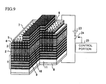
- FIG. 9 is a partially cutaway view in perspective of an example of the optical switch.
- the optical switch is provided with a fixed power source 23 and a switch 24 arranged in series, instead of the variable power source 12 shown in FIG. 1, so that a control portion 25 turns on or off the switch 24.
- the switch 24 is turned on, the current flows through the photonic crystal structure and the refractive index thereof is changed, shifting the wavelength band of the light passing through the optical waveguide of the line defect portion 10.
- the light in the wavelength band which was able to pass through the optical waveguide when the switch is turned off, is interrupted.
- the optical switch capable of performing on/off of the light in a desired wavelength band is realized.
- the on/off signal of the control portion 25 is made to correspond to a modulation signal.
- FIG. 10 is a cross-sectional view of a slab optical waveguide, which is realized by forming only the photonic crystal structure of the variable wavelength filter corresponding to FIG. 1. Since it is not necessary to provide the electrode or to constrict the current in the slab optical waveguide, providing the selective oxidation film 4 and processing the etching for profile formation are not required, as shown in FIG. 10. For this reason, the slab optical waveguide using the photonic crystal structure can be formed with a simple configuration.
- the hole 9 may be formed to pass through all layers of the lower DBR layer 1. Additionally, the hole 9 may be formed so that it is not deeper than the interface between the core layer 2 and the lower DBR layer 1.
- the hole 9 of the photonic crystal structure having the line defect portion 10 is formed at the minimum aspect ratio as required using the semiconductor process, the photonic crystal structure with excellent accuracy can be formed. Moreover, using a semiconductor reflective film such as the lower DBR layer 1, an radiation leaky mode from the two-dimensional photonic crystal structure can be readily inhibited.
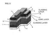
- the core layer 2 is disposed between an upper cladding layer 2a and a lower cladding layer 2b as shown in FIG. 11.
- the upper cladding layer 2a and the lower cladding layer 2b are constituted by such as InGaAsP and the compositions thereof are adjusted so that the energy band gap is greater than the energy band gap of the core layer 2.
- the hole 9 constituting the photonic crystal passes through the upper cladding layer 2a and the core layer 2, and reaches the lower cladding layer 2b, but does not reach the lower DBR layer 1.
- the hole 9 may have the depth which reaches the lower DBR layer 1 like that in FIG. 1.
- an upper portion of the line defect has an optical confinement structure in which the light is reflected vertically and returned to the line defect portion 10 with the upper DBR layer 3 and the dielectric multilayer film 6, and both sides of the line defect portion 10 has an optical confinement structure in which the light in the transverse direction is confined because of the photonic crystal structure having the hole 9. Since the optical confinement in the vertical direction may be weak in a region on both sides of the line defect portion 10, the dielectric multilayer film 6 is not formed in that region. In addition, since the holes 9 are formed only in the upper DBR layer 3, i.e.
- the aspect ratio of the holes 9 can be small.
- the p-electrode 7 is disposed on the upper DBR layer 3 situated in the middle of the upper reflective film, the distance between the p-electrode 7 and the n-electrode 8 is decreased, which reduces a resistance therebetween and the power consumption.
- the light guided through the line defect portion 10 is that in the wavelength band corresponding to the photonic band gap of the photonics crystal.
- the lower DBR layer 1 and the lower cladding layer 2b serve as an n-type layer by an n-type dopant such as silicon (Si) being doped, while the upper DBR layer 3, the upper cladding layer 2a, the selective oxidation layer 4, and the contact layer 5 serve as a p-type layer by a p-type dopant such as zinc (Zn) being doped.
- n-type dopant such as silicon (Si) being doped
- the upper DBR layer 3, the upper cladding layer 2a, the selective oxidation layer 4, and the contact layer 5 serve as a p-type layer by a p-type dopant such as zinc (Zn) being doped.
- FIG. 12 is a cross-sectional view of the semiconductor laser of the second embodiment
- FIG. 13 is a plan view of the semiconductor laser shown in FIG. 12.
- the semiconductor laser is an in-plane resonance type semiconductor laser, wherein a core layer 32 having an active layer 32a constituted by GaInNAsSb is disposed instead of the core layer 2 shown in FIG. 1.
- the semiconductor laser of FIG.12 is different from that in FIG. 1 in that the photonic crystal structure with a point defect portion 30 is formed, instead of the line defect portion 10. That is, as shown in FIG. 13, the point defect portion 30 is formed as a defect of the photonic crystal so that the surrounding structure confines the light two-dimensionally.
- the holes 39 of the photonic crystal are surrounding the point defect portion 30.
- an electrode 37 is shaped in an annular form instead of the stripe form.
- the GaAs substrate is used instead of the n-InP substrate of the foregoing embodiment, and the DBR layers such as the lower DBR layer 1 are constituted by pairs of GaAs/AlGaAs.
- the light in 1310 nm-band excited in the active layer 32a of the point defect portion 30 is resonated between the lower DBR layer 1 and the upper DBR layer 3 plus the dielectric multilayer film 6, so that a laser beam is emitted through the dielectric multilayer film 6.
- the point defect portion 30 may not correspond to a defect of a single hole 39 but may correspond to a plurality of point defects. Moreover, a multiple quantum well structure may be used as the active layer 32a.
- the Q value of the point defect portion 30 according to the second embodiment is approximately 3000 while that of the air-bridge type is approximately 4000. Consequently, it is understood that, in the semiconductor laser shown in the second embodiment, a resonator is formed which is substantially similar to that of the air-bridge type semiconductor laser. Incidentally, the depth of the hole 39 in FIG. 12 may not reach the lower DBR layer 1, like the hole 9 shown in FIG. 8.
- FIG. 14 is a perspective view illustrating a photonic crystal semiconductor device of a third embodiment of the present invention, which is used as a superprism
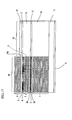
- FIG. 15 is a plan view illustrating a core layer of the photonic crystal semiconductor device shown in FIG. 14.
- like reference numerals as FIGS. 1 and 11 indicate the similar elements.
- the lower DBR layer 1, the lower cladding layer 2b, the core layer 2, the upper cladding layer 2a, the upper DBR layer 3, the selective oxidation layer 4, and the contact layer 5 are formed in that order on the n-InP substrate 11 by the MOCVD method. Further, the stripe-shaped dielectric multilayer film 6 is formed on the contact layer 5 to extend along the direction of the light -guiding. Additionally, on both sides of the dielectric multilayer film 6, the p-electrode 7 is formed on the contact layer 5.
- a plurality of holes 9 are formed in a triangular configuration in the upper DBR layer 3, the upper cladding layer 2a, the core layer 2, and the lower cladding layer 2b, to constitute the photonic crystal structure.
- a point defect portion or a line defect portion is not formed in the photonic crystal structure, unlike with the first and second embodiments.
- the traveling direction of the light can be considerably shifted by slightly changing the wavelength or the incidence angle of the light which enters into the core layer 2. That is, in the photonic crystal, a photonic band structure is formed due to its periodic structure, in which the propagation direction of the light changes sensitively in accordance with the wavelength or the incidence angle thereof.
- the light when the lower portion of the dielectric multilayer film 6 is used as the optical waveguide and the light including a plurality of wavelengths ⁇ 1, ⁇ 2, and ⁇ 3 is entered into one end of the core layer 2 of the optical waveguide, the light is split in accordance with the different wavelengths and emitted from the other end of the core layer 2 at different positions.
- these lights having the different wavelengths are combined and emitted from one position of the one end thereof.
- the photonic crystal semiconductor device in FIG. 14 can be used as an optical coupler/splitter.
- the wavelength band of the light guided in the core layer 2 can be changed.
- the width of the dielectric multilayer film 6 the current flowing from the p-electrode 7 can be guided to the core layer 2 portion under the dielectric film 6.
- FIG. 16 is a perspective cross-sectional view illustrating a photonic crystal optical device integrated with a semiconductor laser, according to a fourth embodiment of the present invention.
- FIG. 17 is a cross-sectional view taken along a line I-I of FIG. 16, and
- FIG. 18 is a cross-sectional view taken along a line II-II of FIG. 16.
- like reference numerals as FIG. 1 indicate the similar elements.
- variable wavelength filter 40 is formed in accordance with the steps described in the first embodiment.
- the variable wavelength filter 40 has the lower DBR layer 1, the lower cladding layer 2b, the core layer 2, the upper cladding layer 2a, the upper DBR layer 3, the selective oxidation layer 4, the contact layer 5, the dielectric multilayer film 6, and the p-electrode 7.
- the semiconductor laser 20 has an n-type cladding layer 14 constituted by n-InP, an active layer 15 having an SCH structure, a p-type cladding layer 16 constituted by p-InP, and a contact layer 17 constituted by p + -InGaAs formed in that order on the n-InP substrate 11 using the MOCVD method. Further, the semiconductor laser 20 has a p-electrode 18 formed on a contact layer 17 for driving the laser. Incidentally, the p-electrode 18 is constituted by Ti/Pt/Au.
- the active layer 15 has the SCH (Separate Confinement Heterostructure) structure, constituted by a multiple quantum well layer and optical confinement layers between which the multiple quantum well layer is disposed.
- the multiple quantum well layer is constituted by a plurality of quantum well layers and barrier layers between which each of the quantum well layers is disposed.
- the quantum well layer and the barrier layer are constituted by InGaAsP having different composition ratios, respectively.
- the optical confinement layer is constituted by InGaAsP whose composition is adjusted so that the energy band gap thereof is greater than that of the barrier layer.
- the semiconductor layers from the n-type cladding layer 14 to the p-type cladding layer 16, which constitute the semiconductor laser 20, are selectively grown while a photonic crystal semiconductor device region is masked with the dielectric film.
- the semiconductor layers from the lower DBR layer 1 to the selective oxidation layer 4, which constitute the photonic crystal semiconductor device 40 are selectively grown while the semiconductor laser region is masked with the dielectric film. Silicon dioxide or silicon nitride, for example, is used as the material for the dielectric film.
- the contact layer 17 of the semiconductor laser 20 and the contact layer 5 of the variable wavelength filter are formed simultaneously, and are separated by a slot 18a formed by means of photolithography technique.
- the n-type cladding layer 14, the active layer 15, and a lower portion of the p-type cladding layer 14, which constitutes the semiconductor laser 20, are patterned in a stripe shape extending in the direction of light-guiding, to have a ridge structure as shown in FIG. 18.
- a p-InP buried layer 19a and an n-InP buried layer 19b are laminated in that order to form a current blocking structure.
- One end of the stripe-shaped active layer 15 is connected to an end of the core layer 2 in the line defect portion 10 of the variable wavelength filter 40.
- the laser beam having a broad wavelength spectrum is emitted from the active layer 15 of the semiconductor laser 20 toward the core layer 2 of the variable wavelength filter 40.
- the variable wavelength filter 40 upon incidence of the laser beam, selects wavelength of the light and guide the selected wavelength of light through the line defect portion 10. The wavelength is selected by adjusting the value of the current flown through the photonic crystal between the n-electrode 8 and the p-electrode 7 of the variable wavelength filter 12.
- the semiconductor laser 20 and the variable wavelength filter 40 are formed on the single n-InP substrate 11, allowing the optical integrated element being microminiaturized.
- the photonic crystal semiconductor device to be integrated with the semiconductor laser 20 on the InP board 11 may be, besides the variable wavelength filter 40, any of the slab waveguide, the optical switch, the optical modulator, and the superprism described in the foregoing embodiments, for example.
Landscapes
- Physics & Mathematics (AREA)
- Optics & Photonics (AREA)
- Engineering & Computer Science (AREA)
- Chemical & Material Sciences (AREA)
- Nonlinear Science (AREA)
- General Physics & Mathematics (AREA)
- Nanotechnology (AREA)
- Life Sciences & Earth Sciences (AREA)
- Biophysics (AREA)
- Crystallography & Structural Chemistry (AREA)
- Microelectronics & Electronic Packaging (AREA)
- Optical Integrated Circuits (AREA)
- Semiconductor Lasers (AREA)
- Optical Modulation, Optical Deflection, Nonlinear Optics, Optical Demodulation, Optical Logic Elements (AREA)
Applications Claiming Priority (2)
| Application Number | Priority Date | Filing Date | Title |
|---|---|---|---|
| JP2004040122 | 2004-02-17 | ||
| PCT/JP2005/002342 WO2005078512A1 (fr) | 2004-02-17 | 2005-02-16 | Dispositif semi-conducteur à cristal photonique et procede pour fabriquer celui-ci |
Publications (3)
| Publication Number | Publication Date |
|---|---|
| EP1722265A1 true EP1722265A1 (fr) | 2006-11-15 |
| EP1722265A8 EP1722265A8 (fr) | 2007-03-21 |
| EP1722265A4 EP1722265A4 (fr) | 2008-07-02 |
Family
ID=34857867
Family Applications (1)
| Application Number | Title | Priority Date | Filing Date |
|---|---|---|---|
| EP05719194A Withdrawn EP1722265A4 (fr) | 2004-02-17 | 2005-02-16 | Dispositif semi-conducteur photonique de cristal et procede pour fabriquer celui-ci |
Country Status (4)
| Country | Link |
|---|---|
| US (1) | US7525726B2 (fr) |
| EP (1) | EP1722265A4 (fr) |
| JP (2) | JP4833665B2 (fr) |
| WO (1) | WO2005078512A1 (fr) |
Cited By (1)
| Publication number | Priority date | Publication date | Assignee | Title |
|---|---|---|---|---|
| WO2019143945A1 (fr) * | 2018-01-18 | 2019-07-25 | Iqe Plc | Réflecteurs de bragg distribués poreux pour des applications laser |
Families Citing this family (24)
| Publication number | Priority date | Publication date | Assignee | Title |
|---|---|---|---|---|
| JP5008874B2 (ja) * | 2005-02-23 | 2012-08-22 | 住友電気工業株式会社 | 受光素子と受光素子を用いた光通信用受信モジュールおよび受光素子を用いた計測器 |
| US7412144B2 (en) * | 2005-07-22 | 2008-08-12 | The United States Of America As Represented By The Secretary Of The Army | Photonic crystal-based optical waveguide modulator |
| JP2007147934A (ja) * | 2005-11-28 | 2007-06-14 | Rohm Co Ltd | 光制御装置およびそれを用いた光制御システム |
| JP2007173353A (ja) * | 2005-12-20 | 2007-07-05 | Kyoto Univ | フォトニック結晶発光ダイオード及びその製造方法 |
| WO2008055409A1 (fr) * | 2006-11-09 | 2008-05-15 | Yiquan Li | Del à surface verticale et à plusieurs couches actives |
| JP2009170508A (ja) * | 2008-01-11 | 2009-07-30 | Furukawa Electric Co Ltd:The | 面発光半導体レーザ及びその製造方法 |
| JP5188259B2 (ja) * | 2008-05-02 | 2013-04-24 | キヤノン株式会社 | 3次元フォトニック結晶を用いた発光素子 |
| KR101799521B1 (ko) * | 2011-05-24 | 2017-11-20 | 삼성전자 주식회사 | 광결정형 광변조기 및 이를 구비하는 3차원 영상 획득 장치 |
| CN204258035U (zh) | 2012-05-31 | 2015-04-08 | 古河电气工业株式会社 | 半导体激光器模块 |
| US9042418B2 (en) * | 2013-02-11 | 2015-05-26 | California Institute Of Technology | III-V photonic crystal microlaser bonded on silicon-on-insulator |
| EP3521920B1 (fr) * | 2016-09-29 | 2021-09-29 | Panasonic Intellectual Property Management Co., Ltd. | Dispositif de balayage optique, dispositif de réception de lumière et système de détection optique |
| DE102016014938B4 (de) * | 2016-12-14 | 2019-06-27 | Forschungsverbund Berlin E.V. | Lichtemittervorrichtung, basierend auf einem photonischen Kristall mit säulen- oder wandförmigen Halbleiterelementen, und Verfahren zu deren Betrieb und Herstellung |
| JP7090861B2 (ja) * | 2017-02-28 | 2022-06-27 | 学校法人上智学院 | 光デバイスおよび光デバイスの製造方法 |
| JP7333666B2 (ja) * | 2017-02-28 | 2023-08-25 | 学校法人上智学院 | 光デバイスおよび光デバイスの製造方法 |
| DE102020200468A1 (de) * | 2020-01-16 | 2021-07-22 | OSRAM Opto Semiconductors Gesellschaft mit beschränkter Haftung | Halbleiterlaserdiode und verfahren zur herstellung einer halbleiterlaserdiode |
| CN111916999B (zh) * | 2020-07-13 | 2022-04-19 | 清华大学 | 具有槽结构的分布式反馈激光器及制备方法 |
| CN111916998A (zh) * | 2020-07-13 | 2020-11-10 | 清华大学 | 基于w3光子晶体缺陷波导的分布式反馈激光器及制备方法 |
| CN111917000A (zh) * | 2020-07-13 | 2020-11-10 | 清华大学 | 具有微腔结构的分布式反馈激光器及制备方法 |
| CN111916997B (zh) * | 2020-07-13 | 2023-11-28 | 清华大学 | 基于空气孔的分布式反馈激光器及制备方法 |
| JP7485284B2 (ja) * | 2020-07-14 | 2024-05-16 | 国立大学法人京都大学 | フォトニック結晶面発光レーザ素子 |
| GB2612040B (en) | 2021-10-19 | 2025-02-12 | Iqe Plc | Porous distributed Bragg reflector apparatuses, systems, and methods |
| JP2023066877A (ja) * | 2021-10-29 | 2023-05-16 | ローム株式会社 | 光センサ及び光センサに備わるバンドパスフィルタ |
| JP7546120B1 (ja) * | 2023-07-31 | 2024-09-05 | Nttイノベーティブデバイス株式会社 | 平面光波回路 |
| CN118981065B (zh) * | 2024-08-06 | 2025-10-03 | 中国计量大学 | 一种基于一维缺陷光子晶体堆叠的太赫兹吸收谱器件及其制备方法 |
Family Cites Families (23)
| Publication number | Priority date | Publication date | Assignee | Title |
|---|---|---|---|---|
| JP3285426B2 (ja) * | 1993-08-04 | 2002-05-27 | 株式会社日立製作所 | 半導体光集積素子及びその製造方法 |
| FR2734097B1 (fr) * | 1995-05-12 | 1997-06-06 | Thomson Csf | Laser a semiconducteurs |
| JPH10284806A (ja) * | 1997-04-10 | 1998-10-23 | Canon Inc | フォトニックバンド構造を有する垂直共振器レーザ |
| US6134043A (en) | 1998-08-11 | 2000-10-17 | Massachusetts Institute Of Technology | Composite photonic crystals |
| US6468823B1 (en) * | 1999-09-30 | 2002-10-22 | California Institute Of Technology | Fabrication of optical devices based on two dimensional photonic crystal structures and apparatus made thereby |
| US6499888B1 (en) * | 1999-12-20 | 2002-12-31 | Corning Lasertron, Inc. | Wide ridge pump laser |
| JP2001257425A (ja) * | 2000-03-13 | 2001-09-21 | Matsushita Electric Ind Co Ltd | 半導体レーザ素子及びその製造方法 |
| JP2002064244A (ja) * | 2000-06-06 | 2002-02-28 | Furukawa Electric Co Ltd:The | 分布帰還型半導体レーザ素子 |
| US6674949B2 (en) * | 2000-08-15 | 2004-01-06 | Corning Incorporated | Active photonic crystal waveguide device and method |
| GB2366666B (en) * | 2000-09-11 | 2002-12-04 | Toshiba Res Europ Ltd | An optical device and method for its manufacture |
| DK1371120T3 (da) * | 2001-03-09 | 2013-07-22 | Alight Photonics Aps | Bølgetypekontrol ved anvendelse af transversal båndgabsstruktur i vcsels |
| JP2002303836A (ja) * | 2001-04-04 | 2002-10-18 | Nec Corp | フォトニック結晶構造を有する光スイッチ |
| US6574383B1 (en) * | 2001-04-30 | 2003-06-03 | Massachusetts Institute Of Technology | Input light coupler using a pattern of dielectric contrast distributed in at least two dimensions |
| US6560006B2 (en) * | 2001-04-30 | 2003-05-06 | Agilent Technologies, Inc. | Two-dimensional photonic crystal slab waveguide |
| JP2003131028A (ja) * | 2001-08-14 | 2003-05-08 | Autocloning Technology:Kk | 光回路 |
| JP3729134B2 (ja) | 2002-01-29 | 2005-12-21 | 松下電器産業株式会社 | 光ピックアップ用2波長半導体レーザ光源 |
| US6829281B2 (en) * | 2002-06-19 | 2004-12-07 | Finisar Corporation | Vertical cavity surface emitting laser using photonic crystals |
| JP2004037938A (ja) * | 2002-07-04 | 2004-02-05 | Furukawa Electric Co Ltd:The | 光素子 |
| JP4569942B2 (ja) * | 2002-09-26 | 2010-10-27 | 三菱電機株式会社 | 光アクティブデバイス |
| US6943377B2 (en) * | 2002-11-21 | 2005-09-13 | Sensor Electronic Technology, Inc. | Light emitting heterostructure |
| US7136561B2 (en) * | 2003-03-26 | 2006-11-14 | Tdk Corporation | Two-dimensional photonic crystal, and waveguide and resonator using the same |
| US7250635B2 (en) * | 2004-02-06 | 2007-07-31 | Dicon Fiberoptics, Inc. | Light emitting system with high extraction efficency |
| JP2005274927A (ja) * | 2004-03-24 | 2005-10-06 | Furukawa Electric Co Ltd:The | フォトニック結晶デバイス |
-
2005
- 2005-02-16 EP EP05719194A patent/EP1722265A4/fr not_active Withdrawn
- 2005-02-16 WO PCT/JP2005/002342 patent/WO2005078512A1/fr not_active Ceased
- 2005-02-16 JP JP2005518034A patent/JP4833665B2/ja not_active Expired - Fee Related
-
2006
- 2006-08-17 US US11/505,428 patent/US7525726B2/en not_active Expired - Fee Related
-
2011
- 2011-02-21 JP JP2011034888A patent/JP2011138156A/ja active Pending
Cited By (4)
| Publication number | Priority date | Publication date | Assignee | Title |
|---|---|---|---|---|
| WO2019143945A1 (fr) * | 2018-01-18 | 2019-07-25 | Iqe Plc | Réflecteurs de bragg distribués poreux pour des applications laser |
| CN111630735A (zh) * | 2018-01-18 | 2020-09-04 | Iqe公司 | 用于激光器应用的多孔分布式布拉格反射器 |
| US11201451B2 (en) | 2018-01-18 | 2021-12-14 | Iqe Plc | Porous distributed Bragg reflectors for laser applications |
| CN111630735B (zh) * | 2018-01-18 | 2024-07-26 | Iqe公司 | 用于激光器应用的多孔分布式布拉格反射器 |
Also Published As
| Publication number | Publication date |
|---|---|
| US20070013991A1 (en) | 2007-01-18 |
| EP1722265A4 (fr) | 2008-07-02 |
| JP2011138156A (ja) | 2011-07-14 |
| EP1722265A8 (fr) | 2007-03-21 |
| US7525726B2 (en) | 2009-04-28 |
| WO2005078512A1 (fr) | 2005-08-25 |
| JPWO2005078512A1 (ja) | 2008-01-17 |
| JP4833665B2 (ja) | 2011-12-07 |
Similar Documents
| Publication | Publication Date | Title |
|---|---|---|
| US7525726B2 (en) | Photonic crystal semiconductor device and production method thereof | |
| KR100759603B1 (ko) | 수직 공진기형 면발광 레이저 장치 | |
| KR101834015B1 (ko) | 하이브리드 수직공진 레이저 | |
| JP4569942B2 (ja) | 光アクティブデバイス | |
| CN101765949B (zh) | 微谐振器系统及其制造方法 | |
| JP4761426B2 (ja) | 光デバイスおよび半導体レーザ発振器 | |
| US7697586B2 (en) | Surface-emitting laser | |
| CN103597676B (zh) | 反射率调制光栅反射镜 | |
| US20070201527A1 (en) | Vertical cavity surface emitting laser | |
| JP4954992B2 (ja) | 半導体光反射素子及び該半導体光反射素子を用いる半導体レーザ及び該半導体レーザを用いる光トランスポンダ | |
| JP2005538532A (ja) | 傾斜型共振器半導体レーザー(tcsl)及びその製造方法 | |
| KR102368946B1 (ko) | 파장 가변 레이저 장치 및 이를 제조하는 방법 | |
| US10243330B2 (en) | Optoelectronic device with resonant suppression of high order optical modes and method of making same | |
| JP2008098379A (ja) | 2次元フォトニック結晶面発光レーザおよびその製造方法 | |
| EP4203207B1 (fr) | Lasers à rétroaction répartie et procédés de fabrication de tels lasers | |
| US11557876B2 (en) | Semiconductor laser | |
| JP2008218549A (ja) | 半導体導波路素子及び半導体レーザ及びその作製方法 | |
| JP2006041013A (ja) | 光制御素子、発光素子、光回路装置 | |
| JPS61212082A (ja) | 集積型半導体レ−ザ | |
| JP2017139341A (ja) | 光素子、集積型光素子および光素子モジュール |
Legal Events
| Date | Code | Title | Description |
|---|---|---|---|
| PUAI | Public reference made under article 153(3) epc to a published international application that has entered the european phase |
Free format text: ORIGINAL CODE: 0009012 |
|
| 17P | Request for examination filed |
Effective date: 20060824 |
|
| AK | Designated contracting states |
Kind code of ref document: A1 Designated state(s): DE FR GB |
|
| RAP1 | Party data changed (applicant data changed or rights of an application transferred) |
Owner name: BABA, TOSHIHIKO Owner name: FURUKAWA ELECTRIC CO., LTD. |
|
| RAP1 | Party data changed (applicant data changed or rights of an application transferred) |
Owner name: FURUKAWA ELECTRIC CO., LTD. Owner name: BABA, TOSHIHIKO |
|
| RAP1 | Party data changed (applicant data changed or rights of an application transferred) |
Owner name: BABA, TOSHIHIKO Owner name: THE FURUKAWA ELECTRIC CO., LTD. |
|
| DAX | Request for extension of the european patent (deleted) | ||
| RBV | Designated contracting states (corrected) |
Designated state(s): DE FR GB |
|
| A4 | Supplementary search report drawn up and despatched |
Effective date: 20080604 |
|
| RAP1 | Party data changed (applicant data changed or rights of an application transferred) |
Owner name: THE FURUKAWA ELECTRIC CO., LTD. Owner name: BABA, TOSHIHIKO |
|
| RIN1 | Information on inventor provided before grant (corrected) |
Inventor name: BABA, TOSHIHIKO Inventor name: KISE, TOMOFUMI,C/O THE FURUKAWA ELECTRIC CO., LTD Inventor name: KIMOTO, TATSUYA,THE FURUKAWA ELECTRIC CO., LTD. Inventor name: YOKOUCHI, NORIYUKI,THE FURUKAWA ELECTRIC CO.,LTD |
|
| 17Q | First examination report despatched |
Effective date: 20110526 |
|
| STAA | Information on the status of an ep patent application or granted ep patent |
Free format text: STATUS: THE APPLICATION IS DEEMED TO BE WITHDRAWN |
|
| 18D | Application deemed to be withdrawn |
Effective date: 20140902 |