EP1722484A2 - Appareil de communication mobile - Google Patents
Appareil de communication mobile Download PDFInfo
- Publication number
- EP1722484A2 EP1722484A2 EP06017561A EP06017561A EP1722484A2 EP 1722484 A2 EP1722484 A2 EP 1722484A2 EP 06017561 A EP06017561 A EP 06017561A EP 06017561 A EP06017561 A EP 06017561A EP 1722484 A2 EP1722484 A2 EP 1722484A2
- Authority
- EP
- European Patent Office
- Prior art keywords
- variable gain
- low pass
- pass filter
- offset voltage
- signal
- Prior art date
- Legal status (The legal status is an assumption and is not a legal conclusion. Google has not performed a legal analysis and makes no representation as to the accuracy of the status listed.)
- Granted
Links
Images








Classifications
-
- H—ELECTRICITY
- H04—ELECTRIC COMMUNICATION TECHNIQUE
- H04B—TRANSMISSION
- H04B1/00—Details of transmission systems, not covered by a single one of groups H04B3/00 - H04B13/00; Details of transmission systems not characterised by the medium used for transmission
- H04B1/38—Transceivers, i.e. devices in which transmitter and receiver form a structural unit and in which at least one part is used for functions of transmitting and receiving
- H04B1/40—Circuits
-
- H—ELECTRICITY
- H04—ELECTRIC COMMUNICATION TECHNIQUE
- H04B—TRANSMISSION
- H04B1/00—Details of transmission systems, not covered by a single one of groups H04B3/00 - H04B13/00; Details of transmission systems not characterised by the medium used for transmission
- H04B1/06—Receivers
- H04B1/16—Circuits
- H04B1/30—Circuits for homodyne or synchrodyne receivers
-
- H—ELECTRICITY
- H03—ELECTRONIC CIRCUITRY
- H03K—PULSE TECHNIQUE
- H03K21/00—Details of pulse counters or frequency dividers
- H03K21/16—Circuits for carrying over pulses between successive decades
-
- H—ELECTRICITY
- H03—ELECTRONIC CIRCUITRY
- H03D—DEMODULATION OR TRANSFERENCE OF MODULATION FROM ONE CARRIER TO ANOTHER
- H03D2200/00—Indexing scheme relating to details of demodulation or transference of modulation from one carrier to another covered by H03D
- H03D2200/0041—Functional aspects of demodulators
- H03D2200/0047—Offset of DC voltage or frequency
Definitions
- the present invention relates generally to a mobile communication apparatus which can be implemented with a less number of components, and more particularly, to a transceiver which employs a direct conversion scheme suitable for larger scale of integration.
- transceiver With explosive popularization of mobile communication apparatus, requirements for a reduction in size and cost have been increased. For this reason, it is desired to eliminate VCO (voltage controlled oscillator), reduce the number of filters, and apply integrated circuits with a higher degree of integration.
- VCO voltage controlled oscillator
- a prior art example of a transceiver which meets such requirements is described in K. Takikawa et. al., "RF Circuits Technique of Dual-Band Transceiver IC for GSM and DCS1800 applications," IEEE 25th European Solid-State Circuits Conference Preprints pp. 278-281, 1999 .
- the configuration of this transceiver is illustrated in Fig. 10A.
- the illustrated transceiver comprises an integrated circuit 1016, and other components 1001 - 1015 which are connected external to the integrated circuit 1016.
- the prior art example supports two frequency bands, i.e., 900 MHz band and 1.8 GHz band.
- the transceiver employs a superheterodyne scheme for a receiver and an offset PLL scheme for a transmitter.
- the superheterodyne receiver requires two RF (high frequency) filters 1001, 1002 for suppressing out-of-band blocker signals; two image rejection filters 1003, 1004 for rejecting blocker signals in an image frequency band associated with mixing; and an IF (intermediate frequency) filter 1005 for filtering out blocker signals near a reception channel.
- the receiver also requires two local oscillators 1006, 1007 for supporting the two frequency bands, i.e., 900 MHz band and 1.8 GHz band.
- a reception scheme which can reduce the number of externally connected components is a direct conversion scheme.
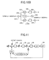
- a prior art example of a direct conversion receiver is described in Behzad Razavi, "A 900-MHz CMOS Direct Conversion Receiver," IEEE Symposium on VLSI Circuits, pp. 113-114, 1997 . The configuration of this receiver is illustrated in Fig. 10B. Since no image response exists in principle, the direct conversion scheme does not require an image rejection filter. Also, an IF filter is eliminated since it can be replaced by a filter integrated in an IC. In this prior art example, a VCO 1025 oscillates at a frequency twice an input frequency of the receiver which is in a range of 1850 - 1920 MHz.
- the VCO 1025 When this receiver is applied to GSM, DCS1800 dual band receiver, the VCO 1025 must oscillate in a range of 1850 to 1920 MHz (for GSM) and in a range of 3610 to 3760 MHz (for DCS1800). However, since it is difficult for a single VCO to cover these frequency bands, two VCOs are required.
- a widely known drawback of the direct conversion receiver is a DC offset voltage. This is generated because an input signal to mixers 1019, 1020 is equal to a locally oscillated signal in frequency. For example, if the locally oscillated signal leaks into an input terminal for an input signal, locally oscillated signals are mutually multiplied to generate DC offset voltage.
- a prior art example of a scheme for canceling the DC offset voltage is described in Asad A. Abidi et. al,. "Direct-Conversion Radio Transceivers for Digital Communications," IEEE Journal of Solid-State Circuits, pp. 1399-1410, vol. 30, no. 12. Dec. 1995 . The configuration of this transceiver is illustrated in Fig. 11.
- An output DC offset voltage of a variable gain amplifier composed of variable gain amplifiers 1101, 1103, 1105 and low pass filters 1102, 1104 is detected by a digital signal processor (DSP) 1106.
- the DSP 1106 outputs a DC offset voltage cancel signal to an input of the variable gain amplifier 1101 based on the detected information.
- the number of externally connected filters can be reduced.
- the direct conversion receiver is used in place of the superheterodyne receiver in the GSM, DCS1800 dual band transceiver of Fig. 10A, the number of local oscillators is increased. This is because the transmitter requires a locally oscillated frequency in a range of 1150 to 1185 MHz (for GSM) and in a range of 1575 to 1650 MHz (for DCS1800), and the receiver requires a locally oscillated frequency in a range of 1850 to 1920 MHz (for GSM) and in a range of 3610 to 3760 MHz (for DCS1800), but a single VCO encounters difficulties in covering a plurality of bands. For a further reduction in cost, a reduction in the number of VCOs is a primary subject.
- GPRS General Packet Radio Service
- a plurality of slots are assigned to reception and transmission.
- fast DC offset voltage cancellation is required.
- the DC offset voltage cancellation must be performed every operation frame.
- One frame of GSM is comprised of eight slots, each of which has a duration of 577 ⁇ m. Assume herein a severe condition for the DC offset voltage cancellation, in which four slots are assigned to the reception (RX), and one slot is assigned to the transmission (TX).
- While a transmission slot TX1' is assigned to a slot 7, the transmission slot TX1' is transmitted at a timing of TX1, which is 237 ⁇ sec before the slot 7, in consideration of a propagation delay to a base station. Also, a monitoring period of approximately 500 ⁇ sec and a PLL synchronizing period are required other than transmission and reception. Assuming that the PLL synchronizing period lasts approximately 150 ⁇ sec, a time available for canceling the DC offset voltage, in which a transceiver does not operate, is calculated as 1154-500-237-150*2 117 ⁇ sec, thus requiring fast DC offset cancellation.
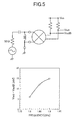
- Fig. 5 shows a measuring circuit for measuring a received frequency dependency of an output DC offset voltage of a mixer, and the result of a measurement made thereby. The result of the measurement reveals that the output DC offset voltage has the frequency dependency. Therefore, in a system such as GSM, DCS1800, in which a received frequency is not fixed during a call but the frequency hops within a reception band, it is difficult to previously anticipate the DC offset voltage. Therefore, the DC offset voltage must be canceled every operation frame.
- a receiver and a transmitter are supplied with locally oscillated signals in an RF band from a single VCO utilizing dividers.
- Dividers each having a fixed division ratio are used for generating the locally oscillated signals for the receiver, while a divider having a switchable division ratio is used for generating the locally oscillated signal for the transmitter.
- a variable gain amplifier for baseband signal is provided with a DC offset voltage detector and a DC offset canceling circuit to accomplish fast cancellation of a DC offset by eliminating intervention of a filter within a feedback loop for offset cancellation.
- the first embodiment uses an exemplary mobile communication apparatus, as an application, which supports the European cellular telephone GSM (900 MHz band) and DCS1800 (1800 MHz band).
- GSM European cellular telephone
- DCS1800 1800 MHz band
- a direct conversion scheme is applied to a receiver for converting an RF signal directly to a baseband signal, and the offset PLL scheme, previously shown in the prior art example, is applied to a transmitter.
- the receiver comprises low noise amplifiers 101, 102; mixers 103, 104; and a variable gain low pass filter 139.
- Each of the mixers converts a signal frequency band from the RF band to the baseband, and simultaneously performs demodulation for separating an RF signal into a sine component and a cosine component.
- the mixers 103, 104 must be applied with locally oscillated signals which are shifted in phase by 90°.
- the locally oscillated signals are generated using dividers 105, 115.
- the locally oscillated signals are generated by a PLL loop formed of a VCO 111 and a PLL 112.
- a VCO for oscillating in a 3600 MHz band is used for the VCO 111
- the output of the divider 115 is in a 1800 MHz band and provides a locally oscillated signal for DCS1800.
- an output frequency of the divider 105 is in a 900 MHz band and provides a locally oscillated signal for GSM.
- Output baseband signals of the mixers 103, 104 are inputted to a variable gain low pass filter 139 for level adjustment and blocker signal rejection.
- the variable gain low pass filter 139 comprises low pass filters 106, 107, 137, 138, and variable gain amplifiers 108, 109. Also, for suppressing a DC offset voltage at the output of the variable gain low pass filter 139, a DC offset voltage canceling circuit 110 is provided.
- the DC offset voltage canceling circuit 110 has a DC offset voltage detecting unit and a DC offset canceling unit.
- fr G 925 MHz
- ft G 880 MHz
- fr D 1805 MHz
- ft D 1710 MHz.
- the IF frequency fIF G calculated for m is shown in Fig. 12
- the IF frequency fIF D calculated for n is shown in Fig. 13. Since a divide-by-two divider is used for the frequency division, 2 to the i-th power (i is an integer number) is used for m and n .
- m and n cannot be freely selected but must be selected such that fIF G is substantially equal to fIF D .
- the ratio of fIF G to fIF D may be substantially equal to 2 to the j-th power (j is an integer number).
- substantially equal means that the two frequencies may be included within an oscillating frequency range of the VCO even if they are not exactly the same.
- the IF frequencies fIF are eventually determined from such combinations of m and n in consideration of power consumption, the presence or absence of generation of an unwanted spurious signal, and so on.
- a combination (m, n) (4,2) is chosen.
- Dividers 117, 118 and a change-over switch 121 are provided subsequent to the VCO 111, and are controlled to divide the output frequency of VCO 111 by four for GSM and by two for DCS1800.
- the oscillating frequency of the VCO 114 is determined depending on the power consumption, the scale of passive elements contained in IC, and so on.
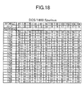
- Figs. 17, 18 show the spurious when the IF frequency is fixed, and the locally oscillated frequency is changed.
- Figs. 17, 18, which correspond to GSM and DSC1800 show the spurious which results from the difference between an integer multiple (multiplied by m) of the IF frequency and the locally oscillated frequency when transmission signals are generated from transmission oscillators 128, 124.
- fIF represents the IF frequency
- fVCO the transmission frequency.
- a numerical value written in each field shows the difference between a spurious signal and the transmission frequency in units of MHz. Hatched fields indicate the spurious generated nearby within 10 MHz, which are not easily removed by a loop filter 127 of the transmitter.
- the spurious can be avoided by selecting the IF frequency at 45 MHz from 880 MHz to 888 MHz and selecting the IF frequency at 46 MHz from 888 MHz to 914 MHz.
- the locally oscillated signal applied to the mixer 126 in the transmitter exists within the reception band.
- Fig. 16 illustrates the transmitter of this embodiment in an enlarged view.
- the locally oscillated signal existing within the reception band leaks through a path designated by 2309, and amplified by an amplifier at a later stage and irradiated.
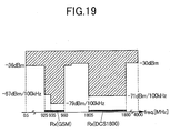
- a standard related to the irradiation of the spurious in GSM is summarized in Fig. 19. While the spurious within the reception band is allowed only at five points and at a level of -36 dBm or lower, it is desired to suppress the spurious to -79 dBm/100kHz in principle.
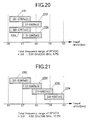
- Fig. 20 summarizes the oscillating frequencies of the VCO so far explained in the foregoing embodiment.
- a reception band 2701 and a transmission band 2703 for DCS1800 are coincident, and a reception band 2702 and a transmission band 2704 for GSM are coincident as well.
- a transmission band 2705 shifted from the reception band 2701 for DCS1800 does not overlap the reception band 2701, so that the leakage of the locally oscillated frequency within the reception band during transmission can be avoided. The same is applied to GSM as well.
- the illustrated receiver comprises a low noise amplifier 102; a mixer 104; a divider 105; low pass filters 106, 137; variable gain amplifiers 108, 201; DC offset voltage canceling circuits 110; and a decoder 205.
- the low noise amplifier 102 in turn comprises a load resistor 207; a transistor 208; and a capacitance 209, while the DC offset voltage canceling circuit 110 comprises a digital-to-analog converter (DAC) 202; an analog-to-digital converter (ADC) 203; and a controller 204.
- the mixer 104 comprises mixers 210, 206.
- An output DC voltage of the variable gain amplifier 108 is converted to a digital signal by the ADC 203, and inputted to the controller 204.
- the controller 204 measures the DC offset voltage at the output of the variable gain amplifier 108 to output a cancel signal for canceling the DC offset voltage.
- the cancel signal is converted from a digital signal to an analog signal by the DAC 202, and an output signal of the DAC 202 cancels the DC offset voltage of the variable gain amplifier 108.
- the decoder 205 selects one of the DC offset voltage canceling circuits 110, such that only the selected circuit is operative.
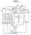
- variable gain amplifier and a DC offset voltage canceling circuit according to a third embodiment of the present invention will be described with reference to Fig. 3.
- the variable gain amplifier comprises resistors 307, 308, 312; and transistors 309, 310, 311.
- the transistors 309, 310 are applied with an input voltage at their bases to deliver output voltages from their collectors.
- the gain can be controlled, for example, by a base voltage of the transistor 311.
- a DAC 313 comprises transistors 301, 302, 303; and resistors 304, 305, 306. Since the output of a controller 204 is connected to bases of the transistors 301, 302, 303, the controller 204 can control collector DC currents of the transistors 301, 302, 303.
- the collector DC currents are summed with a collector current of the transistor 309, and then converted to a voltage by the resistor 307.
- Fig. 6A illustrates an ideal variable gain amplifier 603 free from a DC offset voltage, and an input conversion DC offset voltage source 606 for the variable gain amplifier 603.
- Figs. 6B, 6C illustrate configurations in which change-over switches 607, 608, i.e., the third embodiment according to the present invention, are connected to the input and output of the variable gain amplifier 603. Since Fig. 6B is opposite to Fig.
- an output voltage of the offset voltage source 606 is transmitted to an opposite terminal, i.e., to 604 in Fig. 6B and to 605 in Fig. 6C, while maintaining the connection relationship between the input and output terminals. Therefore, when the aforementioned change-over switches 607, 608 are periodically changed over, the output voltage of the offset voltage source 606 appears at the output terminals 6-04, 605 for the same time, so that the offset voltage between the output terminals becomes zero.
- FIG. 7 shows a receiver characterized in that the variable gain amplifier 609 shown in the third embodiment is employed in place of the variable gain amplifier 201 and the DC offset voltage canceling circuit 206 in the second embodiment, and a low pass filter 702 and a buffer amplifier 701 are connected subsequent to the variable gain amplifier 609.
- FIG. 8 shows a receiver characterized in that a switch 801 is connected between the low pass filter 140 and the variable gain amplifier 201 in the second embodiment.
- the switch 801 is turned on to short-circuit inputs of the variable gain amplifier 201, and the switch 801 is maintained off when the cancellation is not performed.
- the variable gain amplifier 201 can perform the cancellation without being affected by a DC offset voltage from the previous stage.
- FIG. 9 shows a mobile communication apparatus characterized in that a baseband circuit 901 is added to the first embodiment.
- a block 907 includes all circuits other than an antenna 139 and a circuit 143 contained in IC in the first embodiment.
- the baseband circuit 901 performs signal processing such as conversion of received baseband signals 902, 903 to audio signals, conversion of audio signals to transmission baseband signals 905, 906, and so on. Further, the baseband circuit 901 outputs a DC offset cancel starting signal 904 for determining the timing at which a DC offset voltage is canceled in the circuit 143, and inputs the signal 904 to the circuit 143.
- the starting signal is sent before a receiver starts receiving a signal, such that a DC offset generated in the circuit 143 is removed before receiving the signal.
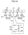
- Switches 1401, 1402 are inserted between a capacitance 1403 and resistors 1404, 1405 in a filter 140 to reduce the time constant during DC offset cancellation. Since this can reduce a propagation delay through the filter 140, the DC offset can be canceled faster without using the input short-circuiting switch 801 illustrated in Fig. 8. Also, when respective amplifiers 108, 201 are comprised of bipolar transistors as illustrated in Fig. 3, the bases of the transistors are biased through filter resistors 1404, 1405. Therefore, the DC offset voltage can be canceled, including a bias offset due to variations in base current and variations in filter resistor.
- the sixth embodiment employing the short-circuiting switch 801 cannot cancel the bias offset.
- a residual error is removed by the DC offset canceling function at a later stage, so that a more accurate DC offset removal can be achieved.
- a mobile communication apparatus according to a ninth embodiment of the present invention will be described with reference to Fig. 15.
- the filter can be interposed in a feedback loop for canceling the DC offset voltage. Therefore, this embodiment can reduce the number of ADCs and accordingly the scale of the circuit, as compared with the eighth embodiment.
- three externally connected filters and one externally connected VCO can be saved as compared with the conventional superheterodyne receiver.
Landscapes
- Engineering & Computer Science (AREA)
- Computer Networks & Wireless Communication (AREA)
- Signal Processing (AREA)
- Transceivers (AREA)
- Measuring Pulse, Heart Rate, Blood Pressure Or Blood Flow (AREA)
- Telephone Function (AREA)
- Amplifiers (AREA)
- Digital Transmission Methods That Use Modulated Carrier Waves (AREA)
- Eye Examination Apparatus (AREA)
- Input Circuits Of Receivers And Coupling Of Receivers And Audio Equipment (AREA)
- Reduction Or Emphasis Of Bandwidth Of Signals (AREA)
- Control Of Motors That Do Not Use Commutators (AREA)
- Circuits Of Receivers In General (AREA)
- Transmitters (AREA)
Applications Claiming Priority (2)
| Application Number | Priority Date | Filing Date | Title |
|---|---|---|---|
| JP32365699 | 1999-11-15 | ||
| EP00124306A EP1102413B1 (fr) | 1999-11-15 | 2000-11-15 | Appareil de communication mobile et multibande |
Related Parent Applications (1)
| Application Number | Title | Priority Date | Filing Date |
|---|---|---|---|
| EP00124306A Division EP1102413B1 (fr) | 1999-11-15 | 2000-11-15 | Appareil de communication mobile et multibande |
Publications (3)
| Publication Number | Publication Date |
|---|---|
| EP1722484A2 true EP1722484A2 (fr) | 2006-11-15 |
| EP1722484A3 EP1722484A3 (fr) | 2007-06-06 |
| EP1722484B1 EP1722484B1 (fr) | 2009-05-27 |
Family
ID=18157152
Family Applications (2)
| Application Number | Title | Priority Date | Filing Date |
|---|---|---|---|
| EP06017561A Expired - Lifetime EP1722484B1 (fr) | 1999-11-15 | 2000-11-15 | Appareil de communication mobile |
| EP00124306A Expired - Lifetime EP1102413B1 (fr) | 1999-11-15 | 2000-11-15 | Appareil de communication mobile et multibande |
Family Applications After (1)
| Application Number | Title | Priority Date | Filing Date |
|---|---|---|---|
| EP00124306A Expired - Lifetime EP1102413B1 (fr) | 1999-11-15 | 2000-11-15 | Appareil de communication mobile et multibande |
Country Status (8)
| Country | Link |
|---|---|
| US (5) | US6826388B1 (fr) |
| EP (2) | EP1722484B1 (fr) |
| JP (1) | JP4566228B2 (fr) |
| KR (2) | KR100765645B1 (fr) |
| AT (2) | ATE432556T1 (fr) |
| DE (2) | DE60042290D1 (fr) |
| NO (2) | NO329890B1 (fr) |
| TW (1) | TW480836B (fr) |
Cited By (1)
| Publication number | Priority date | Publication date | Assignee | Title |
|---|---|---|---|---|
| WO2009049400A1 (fr) * | 2007-10-14 | 2009-04-23 | Nicolson Sean T | Système et procédé destinés à un émetteur- récepteur monopuce de conversion directe en silicium |
Families Citing this family (57)
| Publication number | Priority date | Publication date | Assignee | Title |
|---|---|---|---|---|
| US6826388B1 (en) * | 1999-11-15 | 2004-11-30 | Renesas Technology Corp. | Mobile communication apparatus including dividers in transmitter and receiver |
| US6697611B1 (en) | 2000-11-14 | 2004-02-24 | Intel Corporation | Method and apparatus for performing DC offset cancellation in a receiver |
| US7076225B2 (en) * | 2001-02-16 | 2006-07-11 | Qualcomm Incorporated | Variable gain selection in direct conversion receiver |
| JP3828076B2 (ja) * | 2001-02-21 | 2006-09-27 | 旭化成マイクロシステム株式会社 | 通信装置 |
| KR100390512B1 (ko) * | 2001-06-22 | 2003-07-04 | 엘지전자 주식회사 | 이동통신 단말기의 셀프 콰이어팅 제거장치 |
| US7236757B2 (en) * | 2001-07-11 | 2007-06-26 | Vativ Technologies, Inc. | High-speed multi-channel communications transceiver with inter-channel interference filter |
| US20030112896A1 (en) * | 2001-07-11 | 2003-06-19 | Raghavan Sreen A. | Multi-channel communications transceiver |
| US7295623B2 (en) * | 2001-07-11 | 2007-11-13 | Vativ Technologies, Inc. | High-speed communications transceiver |
| JP3672189B2 (ja) | 2001-07-13 | 2005-07-13 | ソニー株式会社 | 無線信号受信装置及び復調処理回路 |
| EP1294151A1 (fr) * | 2001-09-12 | 2003-03-19 | STMicroelectronics N.V. | Suppression du décalage de composante continue pour un récepteur à conversion directe |
| GB2382242B (en) * | 2001-11-15 | 2005-08-03 | Hitachi Ltd | Direct-conversion transmitting circuit and integrated transmitting/receiving circuit |
| GB0127535D0 (en) * | 2001-11-16 | 2002-01-09 | Hitachi Ltd | A communication semiconductor integrated circuit device and wireless communication system |
| KR100438556B1 (ko) * | 2001-12-10 | 2004-07-02 | 엘지전자 주식회사 | 트라이 모드 이동 단말기에서의 고주파 신호 처리 장치 및방법 |
| JP2005518757A (ja) * | 2002-02-21 | 2005-06-23 | アナログ・デバイシズ・インコーポレーテッド | 3g無線受信機 |
| GB0204108D0 (en) * | 2002-02-21 | 2002-04-10 | Analog Devices Inc | 3G radio |
| US6985711B2 (en) * | 2002-04-09 | 2006-01-10 | Qualcomm, Incorporated | Direct current offset cancellation for mobile station modems using direct conversion |
| DE10219362B4 (de) * | 2002-04-30 | 2009-12-31 | Advanced Micro Devices, Inc., Sunnyvale | Automatische Verstärkungssteuerung für einen Direktumsetzer und Verfahren zum Steuern der Verstärkung eines Basisbandsignals in einem derartigen Empfänger |
| US7307480B2 (en) * | 2002-10-31 | 2007-12-11 | Qualcomm Incorporated | Low latency frequency switching |
| US20070019113A1 (en) * | 2002-12-19 | 2007-01-25 | Jan Van Sinderen | Mixer system with amplitude-, common mode- and phase corrections |
| JP4230762B2 (ja) | 2002-12-20 | 2009-02-25 | 株式会社ルネサステクノロジ | ダイレクトコンバージョン受信機 |
| KR101058973B1 (ko) * | 2003-02-07 | 2011-08-23 | 에스티 에릭슨 에스에이 | 인터페이싱 방법 및 인터페이싱 회로 |
| DE10317598A1 (de) * | 2003-04-16 | 2004-11-25 | Infineon Technologies Ag | Integrierter Transceiverschaltkreis |
| US7146141B2 (en) * | 2003-05-15 | 2006-12-05 | Via Technologies, Inc. | Direct conversion receiver with DC offset compensation and method thereof |
| US7388904B2 (en) * | 2003-06-03 | 2008-06-17 | Vativ Technologies, Inc. | Near-end, far-end and echo cancellers in a multi-channel transceiver system |
| US7310505B2 (en) * | 2003-09-09 | 2007-12-18 | Zenith Electronics Corporation | Attenuation control for tuners |
| CN1886901B (zh) * | 2003-12-01 | 2013-12-18 | 松下电器产业株式会社 | 接收装置和半导体集成电路装置 |
| JP4220999B2 (ja) * | 2003-12-01 | 2009-02-04 | パナソニック株式会社 | 受信装置、受信方法及び半導体集積回路装置 |
| JP4234026B2 (ja) * | 2004-01-26 | 2009-03-04 | パナソニック株式会社 | 受信回路 |
| DE102004017527B4 (de) | 2004-04-08 | 2007-10-31 | Infineon Technologies Ag | Transceiverschaltung und Verfahren zur Bereitstellung von Lokaloszillatorsignalen in einer Transceiverschaltung |
| US7266352B2 (en) * | 2004-05-28 | 2007-09-04 | Wionics Research | Multiple band RF transmitters and receivers having independently variable RF and IF local oscillators and independent high-side and low-side RF local oscillators |
| US7835706B2 (en) * | 2004-06-30 | 2010-11-16 | Silicon Laboratories, Inc. | Local oscillator (LO) port linearization for communication system with ratiometric transmit path architecture |
| US7272373B2 (en) * | 2004-06-30 | 2007-09-18 | Silacon Laboratories Inc. | Ratiometric clock systems for integrated receivers and associated methods |
| US7463875B2 (en) * | 2004-09-24 | 2008-12-09 | Samsung Electronics Co., Ltd. | Wireless device minimizing use of external bandpass filter between low-noise amplifier and first mixer |
| US20060068746A1 (en) * | 2004-09-30 | 2006-03-30 | Nokia Corporation | Direct conversion receiver radio frequency integrated circuit |
| US8180312B2 (en) * | 2005-08-04 | 2012-05-15 | Samsung Electronics Co., Ltd. | Receiver architecture for minimizing use of external bandpass filter between low-noise amplifier and first mixer |
| FR2900006B1 (fr) * | 2006-04-13 | 2013-09-20 | St Microelectronics Sa | Recepteur de signal radio, du type a frequence intermediaire |
| US7610026B2 (en) * | 2006-08-11 | 2009-10-27 | Broadcom Corporation | Transmitter non-data-related direct current (DC) offset cancellation scheme |
| US7764124B2 (en) * | 2006-09-26 | 2010-07-27 | Project Ft, Inc. | Broadband low noise amplifier |
| TWI407761B (zh) * | 2006-12-07 | 2013-09-01 | Wistron Neweb Corp | 可同時於複數個行動通訊系統下待機之通訊裝置 |
| JP5179858B2 (ja) * | 2007-01-06 | 2013-04-10 | 株式会社半導体エネルギー研究所 | 半導体装置 |
| US20090031485A1 (en) * | 2007-07-30 | 2009-02-05 | Robert Prusinski | Face Shield for Safety Helmet |
| JP5202213B2 (ja) * | 2008-09-25 | 2013-06-05 | パナソニック株式会社 | 周波数シンセサイザ及び無線送信装置 |
| JP2011124831A (ja) * | 2009-12-11 | 2011-06-23 | Renesas Electronics Corp | 通信装置 |
| JP5611070B2 (ja) | 2011-01-28 | 2014-10-22 | ルネサスエレクトロニクス株式会社 | 半導体集積回路およびその動作方法 |
| US8874062B2 (en) * | 2011-07-01 | 2014-10-28 | Broadcom Corporation | Apparatus for removing DC components inherent in a radio frequency chain |
| JP5778047B2 (ja) * | 2012-01-18 | 2015-09-16 | ルネサスエレクトロニクス株式会社 | 半導体集積回路およびその動作方法 |
| US8787503B2 (en) * | 2012-09-18 | 2014-07-22 | Vixs Systems, Inc. | Frequency mixer with compensated DC offset correction to reduce linearity degradation |
| JP5711718B2 (ja) * | 2012-10-26 | 2015-05-07 | 旭化成エレクトロニクス株式会社 | Ask受信器およびこれを備えるicチップ |
| US9595922B2 (en) * | 2012-11-19 | 2017-03-14 | Infineon Technologies Ag | Chopper amplifier |
| US9184957B2 (en) * | 2012-12-27 | 2015-11-10 | Intel Corporation | High speed receivers circuits and methods |
| CA2814303A1 (fr) | 2013-04-26 | 2014-10-26 | Cellphone-Mate, Inc. | Appareil et procedes pour amplificateurs de signaux de frequence radio |
| WO2015196160A1 (fr) | 2014-06-19 | 2015-12-23 | Project Ft, Inc. | Dispositif actif sans mémoire qui piège les signaux d'harmoniques paires |
| KR101658076B1 (ko) * | 2015-01-19 | 2016-09-30 | 실리콘알엔디(주) | 초광대역 임펄스 수신기의 dc 보정기 및 이를 포함하는 초광대역 임펄스 수신기 |
| US10027355B2 (en) * | 2016-01-19 | 2018-07-17 | Analog Devices Global | Blocker detection based automatic gain control |
| JP2017158085A (ja) * | 2016-03-03 | 2017-09-07 | 株式会社デンソー | 受信装置 |
| KR102653887B1 (ko) * | 2017-01-31 | 2024-04-02 | 삼성전자주식회사 | 가변 피드백 이득을 갖는 델타 변조기, 이를 포함하는 아날로그-디지털 변환기 및 통신 장치 |
| WO2019024976A1 (fr) | 2017-07-31 | 2019-02-07 | Renesas Electronics Corporation | Suppression de décalage |
Family Cites Families (62)
| Publication number | Priority date | Publication date | Assignee | Title |
|---|---|---|---|---|
| FR2316788A1 (fr) * | 1975-07-01 | 1977-01-28 | Commissariat Energie Atomique | Procede et dispositif d'elimination de la tension residuelle d'erreur d'un amplificateur |
| JPS5575313A (en) * | 1978-12-01 | 1980-06-06 | Toshiba Corp | Offset voltage compensating circuit for amplifier |
| US4321561A (en) * | 1979-09-28 | 1982-03-23 | Honeywell Inc. | Switch operated capacitive oscillator apparatus |
| US4633223A (en) * | 1981-10-13 | 1986-12-30 | Intel Corporation | DC offset correction circuit utilizing switched capacitor differential integrator |
| US4731796A (en) * | 1984-10-25 | 1988-03-15 | Stc, Plc | Multi-mode radio transceiver |
| US4940950A (en) * | 1988-08-12 | 1990-07-10 | Tel-Instrument Electronics Corporation | Frequency synthesis method and apparatus using approximation to provide closely spaced discrete frequencies over a wide range with rapid acquisition |
| JPH082058B2 (ja) | 1989-06-13 | 1996-01-10 | 日本電気株式会社 | 自動利得制御方式 |
| US5263194A (en) * | 1990-03-07 | 1993-11-16 | Seiko Corp. | Zero if radio receiver for intermittent operation |
| US5179730A (en) * | 1990-03-23 | 1993-01-12 | Rockwell International Corporation | Selectivity system for a direct conversion receiver |
| JPH0438004A (ja) * | 1990-06-04 | 1992-02-07 | Sumitomo Electric Ind Ltd | 差動増幅回路 |
| US5212826A (en) * | 1990-12-20 | 1993-05-18 | Motorola, Inc. | Apparatus and method of dc offset correction for a receiver |
| JP2850160B2 (ja) * | 1991-01-25 | 1999-01-27 | 松下電器産業株式会社 | 時分割複信無線送受信装置 |
| JP3115050B2 (ja) | 1991-09-11 | 2000-12-04 | 株式会社日立製作所 | 移動通信機 |
| JP3191167B2 (ja) * | 1991-11-15 | 2001-07-23 | 日本電気エンジニアリング株式会社 | 自動オフセット回路 |
| WO1993026094A1 (fr) * | 1992-06-08 | 1993-12-23 | Motorola, Inc. | Commande de gain automatique d'un recepteur |
| JPH06303137A (ja) | 1992-12-29 | 1994-10-28 | Hitachi Ltd | D/a変換器、オフセット調整回路及びこれを用いた携帯通信端末装置 |
| US5580558A (en) * | 1993-11-17 | 1996-12-03 | The Jikei University School Of Medicine | Delivery of gene products via mesangial cells |
| FI941862A7 (fi) | 1994-04-21 | 1995-10-22 | Nokia Mobile Phones Ltd | Menetelmä ja radiotaajuusjärjestelmä kahden eri taajuusalueella toimivan radioviestinjärjestelmän vastaanottimen ja lähettimen taajuuksien muodostamiseksi ja kahdella eri taajuusalueella toimiva vastaanotin ja lähetin sekä edellisten käyttö matkapuhelimessa |
| ZA95605B (en) | 1994-04-28 | 1995-12-20 | Qualcomm Inc | Method and apparatus for automatic gain control and dc offset cancellation in quadrature receiver |
| JPH07303126A (ja) * | 1994-05-02 | 1995-11-14 | Matsushita Electric Ind Co Ltd | 受信装置 |
| US5535432A (en) * | 1994-09-14 | 1996-07-09 | Ericsson Ge Mobile Communications Inc. | Dual-mode satellite/cellular phone with a frequency synthesizer |
| US5471665A (en) * | 1994-10-18 | 1995-11-28 | Motorola, Inc. | Differential DC offset compensation circuit |
| US5724653A (en) * | 1994-12-20 | 1998-03-03 | Lucent Technologies Inc. | Radio receiver with DC offset correction circuit |
| WO1996037951A1 (fr) * | 1995-05-23 | 1996-11-28 | Analog Devices, Inc. | Suppression du decalage d'un condensateur commute |
| JP3425277B2 (ja) * | 1995-08-25 | 2003-07-14 | 株式会社東芝 | 無線受信機 |
| US5748681A (en) * | 1995-10-27 | 1998-05-05 | Lucent Technologies Inc | Offset correction for a homodyne radio |
| JPH09130291A (ja) | 1995-10-31 | 1997-05-16 | Hitachi Ltd | デュアルモード携帯電話端末のクロック分配方式 |
| FR2742946B1 (fr) * | 1995-12-22 | 1998-01-16 | Alcatel Mobile Comm France | Terminal de radiocommunication multimode |
| JPH09261106A (ja) | 1996-03-22 | 1997-10-03 | Matsushita Electric Ind Co Ltd | 複数帯域移動無線機 |
| US5721756A (en) * | 1996-03-26 | 1998-02-24 | Sicom, Inc. | Digital receiver with tunable analog parameters and method therefor |
| FI100286B (fi) * | 1996-04-01 | 1997-10-31 | Nokia Mobile Phones Ltd | Lähetin/vastaanotin RF-signaalin lähettämiseksi ja vastaanottamiseksi kahdella taajuusalueella |
| US6498929B1 (en) * | 1996-06-21 | 2002-12-24 | Kabushiki Kaisha Toshiba | Receiver having DC offset decreasing function and communication system using the same |
| US5732330A (en) * | 1996-07-02 | 1998-03-24 | Ericsson Inc. | Dual band transceiver |
| JP3907703B2 (ja) | 1996-09-06 | 2007-04-18 | コーニンクレッカ フィリップス エレクトロニクス エヌ ヴィ | 零if受信器 |
| US5869987A (en) * | 1996-09-20 | 1999-02-09 | Lucent Technologies, Inc. | Fast response comparator |
| US5689987A (en) * | 1996-09-27 | 1997-11-25 | Mcdonnell Douglas Corporation | Method for determining the proper progress of a superplastic forming process by monitoring gas-mass outflow |
| JPH10200353A (ja) | 1997-01-14 | 1998-07-31 | Kokusai Electric Co Ltd | バーストagc回路およびバーストagc制御方法 |
| JP3731276B2 (ja) * | 1997-03-03 | 2006-01-05 | 三菱電機株式会社 | 受信機 |
| US6006079A (en) * | 1997-06-13 | 1999-12-21 | Motorola, Inc. | Radio having a fast adapting direct conversion receiver |
| US6106519A (en) * | 1997-06-30 | 2000-08-22 | Ethicon Endo-Surgery, Inc. | Capacitively coupled electrosurgical trocar |
| JPH1141131A (ja) * | 1997-07-15 | 1999-02-12 | Toshiba Corp | 無線通信装置 |
| DE19743272C1 (de) * | 1997-09-30 | 1999-02-18 | Siemens Ag | Anordnung und Verfahren zur Kompensation des Offsets eines Mischers |
| FI974269A7 (fi) * | 1997-11-18 | 1999-05-19 | Nokia Mobile Phones Ltd | Kahden taajuusalueen radiolähetin-vastaanotinrakenne |
| US6516187B1 (en) * | 1998-03-13 | 2003-02-04 | Maxim Integrated Products, Inc. | DC offset correction for direct conversion tuner IC |
| EP0948128B1 (fr) * | 1998-04-03 | 2004-12-01 | Motorola Semiconducteurs S.A. | Annulation de décalage DC dans un récepteur à quadrature |
| US6208875B1 (en) * | 1998-04-08 | 2001-03-27 | Conexant Systems, Inc. | RF architecture for cellular dual-band telephones |
| US6073848A (en) * | 1998-05-18 | 2000-06-13 | Symbol Technologies, Inc. | Digital automatic gain control for multi-stage amplification circuits |
| US7035351B1 (en) * | 1998-07-24 | 2006-04-25 | Gct Semiconductor, Inc. | Automatic gain control loop apparatus |
| US6335952B1 (en) * | 1998-07-24 | 2002-01-01 | Gct Semiconductor, Inc. | Single chip CMOS transmitter/receiver |
| US6298226B1 (en) * | 1998-11-30 | 2001-10-02 | Conexant Systems, Inc. | Receiver for RF signals |
| US6353364B1 (en) * | 1998-12-22 | 2002-03-05 | Ericsson Inc. | Digitally gain controllable amplifiers with analog gain control input, on-chip decoder and programmable gain distribution |
| US6484014B1 (en) * | 1999-03-22 | 2002-11-19 | Ericsson Inc. | Reduced component frequency plan architecture for dual band transceiver |
| JP2000286742A (ja) | 1999-03-31 | 2000-10-13 | Toshiba Corp | 無線通信装置 |
| US6166668A (en) * | 1999-06-01 | 2000-12-26 | Motorola, Inc. | Method and apparatus for providing DC offset correction and hold capability |
| FI112561B (fi) * | 1999-06-10 | 2003-12-15 | Nokia Corp | Lähetin/vastaanotin RF-signaalin lähettämiseksi ja vastaanottamiseksi ainakin kahdella taajuusalueella |
| US7555263B1 (en) * | 1999-10-21 | 2009-06-30 | Broadcom Corporation | Adaptive radio transceiver |
| US6826388B1 (en) * | 1999-11-15 | 2004-11-30 | Renesas Technology Corp. | Mobile communication apparatus including dividers in transmitter and receiver |
| US6317064B1 (en) * | 2000-02-29 | 2001-11-13 | Motorola, Inc. | DC offset correction adaptable to multiple requirements |
| US6356217B1 (en) * | 2000-02-29 | 2002-03-12 | Motorola, Inc. | Enhanced DC offset correction through bandwidth and clock speed selection |
| JP3479835B2 (ja) * | 2000-09-13 | 2003-12-15 | 日本電気株式会社 | ベースバンド利得制御方法及びベースバンド利得制御回路 |
| US6560447B2 (en) * | 2001-03-05 | 2003-05-06 | Motorola, Inc. | DC offset correction scheme for wireless receivers |
| JP2003258662A (ja) * | 2002-03-06 | 2003-09-12 | Alps Electric Co Ltd | 2周波数帯域共用コンバータユニット |
-
2000
- 2000-11-14 US US09/711,105 patent/US6826388B1/en not_active Expired - Lifetime
- 2000-11-14 NO NO20005772A patent/NO329890B1/no not_active IP Right Cessation
- 2000-11-15 KR KR1020000067676A patent/KR100765645B1/ko not_active Expired - Lifetime
- 2000-11-15 DE DE60042290T patent/DE60042290D1/de not_active Expired - Lifetime
- 2000-11-15 EP EP06017561A patent/EP1722484B1/fr not_active Expired - Lifetime
- 2000-11-15 AT AT06017561T patent/ATE432556T1/de not_active IP Right Cessation
- 2000-11-15 AT AT00124306T patent/ATE352906T1/de not_active IP Right Cessation
- 2000-11-15 EP EP00124306A patent/EP1102413B1/fr not_active Expired - Lifetime
- 2000-11-15 DE DE60033114T patent/DE60033114T2/de not_active Expired - Lifetime
- 2000-11-15 TW TW089124187A patent/TW480836B/zh not_active IP Right Cessation
-
2003
- 2003-12-23 US US10/742,812 patent/US20040137941A1/en not_active Abandoned
- 2003-12-23 US US10/742,813 patent/US7366489B2/en not_active Expired - Lifetime
-
2007
- 2007-05-07 KR KR1020070044293A patent/KR100756148B1/ko not_active Expired - Lifetime
- 2007-11-14 JP JP2007295286A patent/JP4566228B2/ja not_active Expired - Lifetime
-
2008
- 2008-03-27 US US12/056,576 patent/US7885626B2/en not_active Expired - Fee Related
-
2010
- 2010-12-17 NO NO20101767A patent/NO332862B1/no not_active IP Right Cessation
- 2010-12-22 US US12/975,488 patent/US8107912B2/en not_active Expired - Fee Related
Non-Patent Citations (3)
| Title |
|---|
| ASAD A. ABIDI: "Direct-Conversion Radio Transceivers for Digital Communications", IEEE JOURNAL OF SOLID- STATE CIRCUITS, vol. 30, 12 December 1995 (1995-12-12), pages 1399 - 1410 |
| BEHZAD RAZAVI: "A 900-MHz CMOS Direct Conversion Receive r", IEEE SYMPOSIUM ON VLSI CIRCUITS, 1997, pages 113 - 114 |
| K. TAKIKAWA: "RF Circuits Technique of Dual-Band Transceiver IC for GSM and DCS1800 application s", IEEE 25TH EUROPEAN SOLID-STATE CIRCUITS CONFERENCE PREPRINTS, 1999, pages 278 - 281 |
Cited By (1)
| Publication number | Priority date | Publication date | Assignee | Title |
|---|---|---|---|---|
| WO2009049400A1 (fr) * | 2007-10-14 | 2009-04-23 | Nicolson Sean T | Système et procédé destinés à un émetteur- récepteur monopuce de conversion directe en silicium |
Also Published As
| Publication number | Publication date |
|---|---|
| TW480836B (en) | 2002-03-21 |
| NO332862B1 (no) | 2013-01-28 |
| KR100765645B1 (ko) | 2007-10-10 |
| US20080182538A1 (en) | 2008-07-31 |
| EP1102413A3 (fr) | 2004-03-24 |
| EP1102413A2 (fr) | 2001-05-23 |
| US7885626B2 (en) | 2011-02-08 |
| US20040137853A1 (en) | 2004-07-15 |
| NO20005772L (no) | 2001-05-16 |
| EP1722484A3 (fr) | 2007-06-06 |
| NO20101767L (no) | 2001-05-16 |
| JP4566228B2 (ja) | 2010-10-20 |
| DE60033114T2 (de) | 2007-06-06 |
| US8107912B2 (en) | 2012-01-31 |
| ATE432556T1 (de) | 2009-06-15 |
| US6826388B1 (en) | 2004-11-30 |
| US7366489B2 (en) | 2008-04-29 |
| KR20010051695A (ko) | 2001-06-25 |
| NO329890B1 (no) | 2011-01-17 |
| EP1102413B1 (fr) | 2007-01-24 |
| NO20005772D0 (no) | 2000-11-14 |
| JP2008109680A (ja) | 2008-05-08 |
| KR20070051827A (ko) | 2007-05-18 |
| US20040137941A1 (en) | 2004-07-15 |
| ATE352906T1 (de) | 2007-02-15 |
| DE60033114D1 (de) | 2007-03-15 |
| KR100756148B1 (ko) | 2007-09-05 |
| DE60042290D1 (de) | 2009-07-09 |
| US20110092175A1 (en) | 2011-04-21 |
| EP1722484B1 (fr) | 2009-05-27 |
Similar Documents
| Publication | Publication Date | Title |
|---|---|---|
| EP1102413B1 (fr) | Appareil de communication mobile et multibande | |
| JP4547084B2 (ja) | 移動体通信機および送受信機 | |
| US7272620B1 (en) | Frequency divider with low harmonics | |
| Abidi | Direct-conversion radio transceivers for digital communications | |
| US20060068746A1 (en) | Direct conversion receiver radio frequency integrated circuit | |
| US6351502B1 (en) | RF front-end with multistage stepdown filtering architecture | |
| US8019314B2 (en) | Radio communication apparatus | |
| US20100074303A1 (en) | Wireless Communication Apparatus | |
| US20060128334A1 (en) | Wireless communication receiver | |
| JP2004534454A (ja) | 低漏洩局部発振器システム | |
| US20040147238A1 (en) | Analog demodulator in a low-if receiver | |
| US6021323A (en) | Direct conversion receiver with reduced even order distortion | |
| US20040214548A1 (en) | Mixer circuit with image frequency rejection, in particular for an RFreceiver with zero or low intermediate frequency | |
| KR100273862B1 (ko) | 이중수퍼헤테로다인형수신회로 | |
| KR100696411B1 (ko) | 싱글칩 cmos 송신기/수신기 및 그의 사용방법 | |
| US7088963B2 (en) | Architecture for cordless telephones | |
| JP4385521B2 (ja) | 送受信機 | |
| EP1938462A2 (fr) | Recepteur de conversion directe a melangeur sous-harmonique |
Legal Events
| Date | Code | Title | Description |
|---|---|---|---|
| PUAI | Public reference made under article 153(3) epc to a published international application that has entered the european phase |
Free format text: ORIGINAL CODE: 0009012 |
|
| AC | Divisional application: reference to earlier application |
Ref document number: 1102413 Country of ref document: EP Kind code of ref document: P |
|
| AK | Designated contracting states |
Kind code of ref document: A2 Designated state(s): AT BE CH CY DE DK ES FI FR GB GR IE IT LI LU MC NL PT SE TR |
|
| AX | Request for extension of the european patent |
Extension state: AL LT LV MK RO SI |
|
| RIC1 | Information provided on ipc code assigned before grant |
Ipc: H04B 1/30 20060101AFI20061006BHEP Ipc: H03D 3/00 20060101ALI20070215BHEP |
|
| PUAL | Search report despatched |
Free format text: ORIGINAL CODE: 0009013 |
|
| AK | Designated contracting states |
Kind code of ref document: A3 Designated state(s): AT BE CH CY DE DK ES FI FR GB GR IE IT LI LU MC NL PT SE TR |
|
| AX | Request for extension of the european patent |
Extension state: AL LT LV MK RO SI |
|
| RIC1 | Information provided on ipc code assigned before grant |
Ipc: H03D 3/00 20060101ALI20070430BHEP Ipc: H04B 1/30 20060101AFI20061006BHEP Ipc: H03F 1/30 20060101ALI20070430BHEP |
|
| 17P | Request for examination filed |
Effective date: 20071206 |
|
| 17Q | First examination report despatched |
Effective date: 20080111 |
|
| AKX | Designation fees paid |
Designated state(s): AT BE CH CY DE DK ES FI FR GB GR IE IT LI LU MC NL PT SE TR |
|
| GRAP | Despatch of communication of intention to grant a patent |
Free format text: ORIGINAL CODE: EPIDOSNIGR1 |
|
| RIN1 | Information on inventor provided before grant (corrected) |
Inventor name: TAKIKAWA, KUMIKOC Inventor name: WATANABE, KAZUOC Inventor name: YAMAWAKI, TAIZOC Inventor name: HONGO,TOYOHIKOC Inventor name: TANAKA, SATOSHIC Inventor name: HOTTA, MASAOC Inventor name: KASAHARA, MASUMIC |
|
| GRAS | Grant fee paid |
Free format text: ORIGINAL CODE: EPIDOSNIGR3 |
|
| GRAA | (expected) grant |
Free format text: ORIGINAL CODE: 0009210 |
|
| AC | Divisional application: reference to earlier application |
Ref document number: 1102413 Country of ref document: EP Kind code of ref document: P |
|
| AK | Designated contracting states |
Kind code of ref document: B1 Designated state(s): AT BE CH CY DE DK ES FI FR GB GR IE IT LI LU MC NL PT SE TR |
|
| REG | Reference to a national code |
Ref country code: GB Ref legal event code: FG4D |
|
| REG | Reference to a national code |
Ref country code: CH Ref legal event code: EP |
|
| REG | Reference to a national code |
Ref country code: IE Ref legal event code: FG4D |
|
| REF | Corresponds to: |
Ref document number: 60042290 Country of ref document: DE Date of ref document: 20090709 Kind code of ref document: P |
|
| REG | Reference to a national code |
Ref country code: DE Ref legal event code: R096 Ref document number: 60042290 Country of ref document: DE Effective date: 20090709 |
|
| REG | Reference to a national code |
Ref country code: SE Ref legal event code: TRGR |
|
| PG25 | Lapsed in a contracting state [announced via postgrant information from national office to epo] |
Ref country code: AT Free format text: LAPSE BECAUSE OF FAILURE TO SUBMIT A TRANSLATION OF THE DESCRIPTION OR TO PAY THE FEE WITHIN THE PRESCRIBED TIME-LIMIT Effective date: 20090527 Ref country code: PT Free format text: LAPSE BECAUSE OF FAILURE TO SUBMIT A TRANSLATION OF THE DESCRIPTION OR TO PAY THE FEE WITHIN THE PRESCRIBED TIME-LIMIT Effective date: 20090927 Ref country code: FI Free format text: LAPSE BECAUSE OF FAILURE TO SUBMIT A TRANSLATION OF THE DESCRIPTION OR TO PAY THE FEE WITHIN THE PRESCRIBED TIME-LIMIT Effective date: 20090527 |
|
| NLV1 | Nl: lapsed or annulled due to failure to fulfill the requirements of art. 29p and 29m of the patents act | ||
| PG25 | Lapsed in a contracting state [announced via postgrant information from national office to epo] |
Ref country code: NL Free format text: LAPSE BECAUSE OF FAILURE TO SUBMIT A TRANSLATION OF THE DESCRIPTION OR TO PAY THE FEE WITHIN THE PRESCRIBED TIME-LIMIT Effective date: 20090527 |
|
| PG25 | Lapsed in a contracting state [announced via postgrant information from national office to epo] |
Ref country code: ES Free format text: LAPSE BECAUSE OF FAILURE TO SUBMIT A TRANSLATION OF THE DESCRIPTION OR TO PAY THE FEE WITHIN THE PRESCRIBED TIME-LIMIT Effective date: 20090907 Ref country code: DK Free format text: LAPSE BECAUSE OF FAILURE TO SUBMIT A TRANSLATION OF THE DESCRIPTION OR TO PAY THE FEE WITHIN THE PRESCRIBED TIME-LIMIT Effective date: 20090527 |
|
| PG25 | Lapsed in a contracting state [announced via postgrant information from national office to epo] |
Ref country code: BE Free format text: LAPSE BECAUSE OF FAILURE TO SUBMIT A TRANSLATION OF THE DESCRIPTION OR TO PAY THE FEE WITHIN THE PRESCRIBED TIME-LIMIT Effective date: 20090527 |
|
| PLBE | No opposition filed within time limit |
Free format text: ORIGINAL CODE: 0009261 |
|
| STAA | Information on the status of an ep patent application or granted ep patent |
Free format text: STATUS: NO OPPOSITION FILED WITHIN TIME LIMIT |
|
| 26N | No opposition filed |
Effective date: 20100302 |
|
| REG | Reference to a national code |
Ref country code: DE Ref legal event code: R097 Ref document number: 60042290 Country of ref document: DE Effective date: 20100302 |
|
| PG25 | Lapsed in a contracting state [announced via postgrant information from national office to epo] |
Ref country code: MC Free format text: LAPSE BECAUSE OF NON-PAYMENT OF DUE FEES Effective date: 20091130 |
|
| REG | Reference to a national code |
Ref country code: CH Ref legal event code: PL |
|
| GBPC | Gb: european patent ceased through non-payment of renewal fee |
Effective date: 20091115 |
|
| REG | Reference to a national code |
Ref country code: FR Ref legal event code: ST Effective date: 20100730 |
|
| REG | Reference to a national code |
Ref country code: DE Ref legal event code: R081 Ref document number: 60042290 Country of ref document: DE Owner name: RENESAS ELECTRONICS CORPORATION, JP Free format text: FORMER OWNERS: RENESAS TECHNOLOGY CORP., TOKYO, JP; TTPCOM LTD., ROYSTON, HERTFORDSHIRE, GB Effective date: 20100806 Ref country code: DE Ref legal event code: R081 Ref document number: 60042290 Country of ref document: DE Owner name: TTPCOM LTD., ROYSTON, GB Free format text: FORMER OWNERS: RENESAS TECHNOLOGY CORP., TOKYO, JP; TTPCOM LTD., ROYSTON, HERTFORDSHIRE, GB Effective date: 20100806 |
|
| PG25 | Lapsed in a contracting state [announced via postgrant information from national office to epo] |
Ref country code: CH Free format text: LAPSE BECAUSE OF NON-PAYMENT OF DUE FEES Effective date: 20091130 Ref country code: FR Free format text: LAPSE BECAUSE OF NON-PAYMENT OF DUE FEES Effective date: 20091130 Ref country code: GR Free format text: LAPSE BECAUSE OF FAILURE TO SUBMIT A TRANSLATION OF THE DESCRIPTION OR TO PAY THE FEE WITHIN THE PRESCRIBED TIME-LIMIT Effective date: 20090828 Ref country code: IE Free format text: LAPSE BECAUSE OF NON-PAYMENT OF DUE FEES Effective date: 20091115 Ref country code: LI Free format text: LAPSE BECAUSE OF NON-PAYMENT OF DUE FEES Effective date: 20091130 |
|
| PG25 | Lapsed in a contracting state [announced via postgrant information from national office to epo] |
Ref country code: GB Free format text: LAPSE BECAUSE OF NON-PAYMENT OF DUE FEES Effective date: 20091115 |
|
| PG25 | Lapsed in a contracting state [announced via postgrant information from national office to epo] |
Ref country code: IT Free format text: LAPSE BECAUSE OF FAILURE TO SUBMIT A TRANSLATION OF THE DESCRIPTION OR TO PAY THE FEE WITHIN THE PRESCRIBED TIME-LIMIT Effective date: 20090527 |
|
| PG25 | Lapsed in a contracting state [announced via postgrant information from national office to epo] |
Ref country code: LU Free format text: LAPSE BECAUSE OF NON-PAYMENT OF DUE FEES Effective date: 20091115 |
|
| PG25 | Lapsed in a contracting state [announced via postgrant information from national office to epo] |
Ref country code: TR Free format text: LAPSE BECAUSE OF FAILURE TO SUBMIT A TRANSLATION OF THE DESCRIPTION OR TO PAY THE FEE WITHIN THE PRESCRIBED TIME-LIMIT Effective date: 20090527 |
|
| PG25 | Lapsed in a contracting state [announced via postgrant information from national office to epo] |
Ref country code: CY Free format text: LAPSE BECAUSE OF FAILURE TO SUBMIT A TRANSLATION OF THE DESCRIPTION OR TO PAY THE FEE WITHIN THE PRESCRIBED TIME-LIMIT Effective date: 20090527 |
|
| REG | Reference to a national code |
Ref country code: DE Ref legal event code: R082 Ref document number: 60042290 Country of ref document: DE Representative=s name: BEETZ & PARTNER MBB PATENTANWAELTE, DE Ref country code: DE Ref legal event code: R082 Ref document number: 60042290 Country of ref document: DE Representative=s name: BEETZ & PARTNER MBB PATENT- UND RECHTSANWAELTE, DE Ref country code: DE Ref legal event code: R081 Ref document number: 60042290 Country of ref document: DE Owner name: RENESAS ELECTRONICS CORPORATION, JP Free format text: FORMER OWNERS: RENESAS ELECTRONICS CORP., KAWASAKI-SHI, KANAGAWA, JP; TTPCOM LTD., ROYSTON, HERTFORDSHIRE, GB Ref country code: DE Ref legal event code: R081 Ref document number: 60042290 Country of ref document: DE Owner name: TTPCOM LTD., ROYSTON, GB Free format text: FORMER OWNERS: RENESAS ELECTRONICS CORP., KAWASAKI-SHI, KANAGAWA, JP; TTPCOM LTD., ROYSTON, HERTFORDSHIRE, GB |
|
| PGFP | Annual fee paid to national office [announced via postgrant information from national office to epo] |
Ref country code: SE Payment date: 20191118 Year of fee payment: 20 Ref country code: DE Payment date: 20191130 Year of fee payment: 20 |
|
| REG | Reference to a national code |
Ref country code: DE Ref legal event code: R071 Ref document number: 60042290 Country of ref document: DE |
|
| P01 | Opt-out of the competence of the unified patent court (upc) registered |
Effective date: 20230516 |