EP1746643B1 - Herstellungsverfahren eines MOS-Transistors. - Google Patents
Herstellungsverfahren eines MOS-Transistors. Download PDFInfo
- Publication number
- EP1746643B1 EP1746643B1 EP06291159.9A EP06291159A EP1746643B1 EP 1746643 B1 EP1746643 B1 EP 1746643B1 EP 06291159 A EP06291159 A EP 06291159A EP 1746643 B1 EP1746643 B1 EP 1746643B1
- Authority
- EP
- European Patent Office
- Prior art keywords
- silicon
- substrate
- gate
- process according
- dielectric
- Prior art date
- Legal status (The legal status is an assumption and is not a legal conclusion. Google has not performed a legal analysis and makes no representation as to the accuracy of the status listed.)
- Ceased
Links
Images


Classifications
-
- H—ELECTRICITY
- H10—SEMICONDUCTOR DEVICES; ELECTRIC SOLID-STATE DEVICES NOT OTHERWISE PROVIDED FOR
- H10P—GENERIC PROCESSES OR APPARATUS FOR THE MANUFACTURE OR TREATMENT OF DEVICES COVERED BY CLASS H10
- H10P90/00—Preparation of wafers not covered by a single main group of this subclass, e.g. wafer reinforcement
- H10P90/19—Preparing inhomogeneous wafers
- H10P90/1904—Preparing vertically inhomogeneous wafers
- H10P90/1906—Preparing SOI wafers
- H10P90/1914—Preparing SOI wafers using bonding
- H10P90/1916—Preparing SOI wafers using bonding with separation or delamination along an ion implanted layer, e.g. Smart-cut
-
- H—ELECTRICITY
- H10—SEMICONDUCTOR DEVICES; ELECTRIC SOLID-STATE DEVICES NOT OTHERWISE PROVIDED FOR
- H10W—GENERIC PACKAGES, INTERCONNECTIONS, CONNECTORS OR OTHER CONSTRUCTIONAL DETAILS OF DEVICES COVERED BY CLASS H10
- H10W10/00—Isolation regions in semiconductor bodies between components of integrated devices
- H10W10/10—Isolation regions comprising dielectric materials
- H10W10/181—Semiconductor-on-insulator [SOI] isolation regions, e.g. buried oxide regions of SOI wafers
Definitions
- the invention relates to integrated circuits, and more particularly to MOS type transistors.
- Silicon On Insulator (SOI) -based transistors in particular full-depletion technology, in addition to the advantages of building more compact architecture than a solid silicon substrate, reduce the effects of short channels.
- SOI Silicon On Insulator
- the substrate is made of silicon and is formed on top of a buried oxide layer, generally called BOX Anglo-Saxon ("Buried OXide"). See for example the document US2005 / 0151222 .
- BOX Anglo-Saxon Buried OXide
- the thickness of the silicon film and the buried oxide layer is relatively low. Indeed, the buried oxide layer is generally between 1450 and 4000 ⁇ . This is also the case of the SOI film whose thickness is generally of the order of 200 ⁇ .
- the reduced thickness of the buried oxide layer results in a reduction of the electrostatic coupling between the drain region and the source region, thereby reducing the phenomenon of short channel effects.
- the buried oxide layer is susceptible to attack, which leads to excessive consumption of insulation material for the realization of the STI insulation region ("Shallow Trench Isolation").
- the SOI film is arranged projecting above the buried oxide layer, so that the gate region is also formed laterally on either side of the buried oxide layer. the SOI region, which tends to create parasitic transistors on the SOI flanks covered with the gate material.
- the object of the invention is therefore to overcome the disadvantages of manufacturing techniques of MOS transistors made SOI technology.
- the object of the invention is therefore, according to a first aspect, a method for producing an MOS transistor on an SOI silicon substrate placed on a buried oxide layer, said transistor being formed in an active zone of the substrate delimited by a insulating region, the method comprising the steps described in claim 1.
- the gate by deposition of a gate material on the dielectric material or high permittivity, the latter can be etched selectively with respect to silicon, the active etching of the silicon can then be performed after the wire rack.
- the step of etching silicon carried out according to conventional methods, usually carried out at the beginning of the process and tending to attack the buried oxide layer, is suppressed.
- the grid can be formed on a perfectly flat surface, which avoids the formation of parasitic transistors on the sides of the SOI.
- an ion implantation of germanium is carried out at the location of the future insulating region, the substrate is annealed in such a way as to cause a localized transformation of the silicon-silicon substrate.
- germanium a layer of gate material is deposited on the substrate with the interposition of a gate oxide layer, the gate is etched and etched at the location of the alloy zone. of silicon-germanium so as to remove said alloy, and said dielectric material is deposited in the area of the etched substrate.
- spacers are formed for the grid.
- the deposited dielectric is a dielectric of the same type as that of the spacers.
- the etching step is an isotropic, plasma or wet etching.
- This etching step may be performed so as to etch the silicon-germanium alloy to the underlying oxide layer.
- An integrated circuit not forming part of the invention comprises a MOS transistor comprising a gate region formed above an SOI silicon substrate deposited on an oxide layer buried between mutually opposite zones of a insulating region delimiting an active zone in which the transistor is formed.
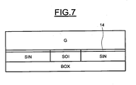
- the upper surface of the insulating region is flush with the upper part of the SOI substrate, so that the gate region is disposed on a flat surface.
- the method consists in producing MOS transistors on a Silicon On Insulator (SOI) type silicon substrate disposed on a BOX buried oxide layer ("Buried OXide").
- SOI Silicon On Insulator
- BOX BOX buried oxide layer
- the buried oxide layer has a thickness of the order of 1500 ⁇ .
- the process step represented on the figure 1 corresponds to an active photolithography phase prior to a deposition of gate material on the SOI substrate.
- the SOI substrate is covered with a photo-sensitive resin layer 10 with the interposition of a hard mask 12 and a layer 13 of nitride Si 3 N 4 .
- this phase of cleaning With reference to the figure 2 before the deposition of the grid material, a cleaning phase must be carried out. As shown in figure 2 , this phase of cleaning generates a non negligible buried oxide BOX up to 100 or even 150 ⁇ thick.
- the gate material is deposited on a non-planar surface, which, as mentioned above, gives rise to the appearance of lateral parasitic transistors.
- the method described in these figures consists in producing MOS transistors on an SOI semiconductor substrate disposed on a buried oxide layer BOX.
- this method allows the realization of transistors on an oxide layer of thickness of the order of 200 ⁇ disposed above a buried oxide layer of thickness also of the order of 200 ⁇ or 100 ⁇ .
- the first phase of the method consists of an implementation of a conventional active photolithography step, during which is deposited, at the location of an area of the substrate intended to constitute the active zone in which a transistor will be formed , a photolithography mask M.
- a photolithography mask M is produced by depositing a resin suitable for the intended use according to a technique known in itself.
- an ion implantation of germanium is carried out in an area of the substrate located at the location of the insulating region R delimiting the active zone.
- the resin is removed and the substrate is then annealed to obtain a localized formation of a silicon-germanium alloy at the location of the isolation region R.
- This phase of forming the grid is performed in a conventional manner and will therefore not be described in detail later.
- gate oxide layer 14 on the SOI substrate, and then depositing a layer of gate material, for example polycrystalline silicon, on the gate oxide layer. This is followed by a photolithography step followed by an etching step, so as to leave only a grid oxide deposit coated with gate material at the gate region for the transistor. to train.
- gate material for example polycrystalline silicon
- the ionic implantation of germanium in the region R of the substrate intended to constitute the insulating region has been carried out so as to subsequently form a localized zone of a silicon-germanium alloy, which may be selectively etched relative to silicon. SOI substrate. Also, alternatively, it is possible to perform localized implantation of any other material that can be selectively etched relative to silicon. However, the use of a silicon-germanium alloy is advantageous insofar as the SiGe alloy zone can then be easily and relatively quickly achieved by conventional techniques.
- the device is in the step visible at the figure 6 wherein a cavity has been created at the silicon-germanium site.
- a dielectric deposit is made to fill the cavities created at the end of the etching step.
- this dielectric may be of the same type as that used for making the spacers E so that the spacers may also be formed during this step.
- the dielectric filling cavity C consists of silicon nitride.
- CVD chemical vapor deposition
- LPCVD low pressure chemical vapor deposition
- the upper face of the insulation region R is flush with the upper face of SOI silicon.
Landscapes
- Thin Film Transistor (AREA)
Claims (7)
- Verfahren zur Herstellung eines MOS-Transistors auf einem Siliciumsubstrat (SOI), angeordnet auf einer Schicht aus vergrabenem Oxid (Buried Oxide = Box), wobei der Transistor in einer aktiven Zone des Substrats hergestellt wird, die durch eine isolierende Region (R) definiert wird, wobei das Verfahren die folgenden Schritte umfasst:1. Definieren der isolierenden Region, die hergestellt wird, indem lokal eine Zone aus einem Material gebildet wird, das bezogen auf Silicium selektiv geätzt werden kann und anschließend2. Herstellen einer Gate-Region (G) und von Source- und Drain-Regionen, die zwischen sich einen Kanal definieren, so dass sich die Gate-Region oberhalb des Kanals erstreckt, und anschließend3. selektives Ätzen des Materials, das bezogen auf Silicium selektiv geätzt werden kann, und Abscheiden eines dielektrischen Materials an der geätzten Stelle.
- Verfahren nach Anspruch 1, dadurch gekennzeichnet, dass eine Germaniumionenimplantation an der Stelle der isolierenden Region (R) durchgeführt wird, das Substrat (SOI) getempert wird, um eine lokale Transformation von Silicium in eine Silicium-Germanium-Legierung zu bewirken, auf dem Substrat eine Schicht aus Gate-Material abgeschieden wird, mit Zwischenschaltung einer Gate-Oxidschicht (14), ein Schritt zum Ätzen an der Stelle der Silicium-Germanium-Legierungszone durchgeführt wird, um die Legierung zu entfernen, und das dielektrische Material in der geätzten Zone abgeschieden wird.
- Verfahren nach Anspruch 2, dadurch gekennzeichnet, dass vor dem Ätzen des Silicium-Germaniums Spacer (E) für das Gate gebildet werden.
- Verfahren nach Anspruch 3, dadurch gekennzeichnet, dass das abgeschiedene Dielektrikum ein Dielektrikum vom gleichen Typ wie das der Spacer ist.
- Verfahren nach einem der Ansprüche 2 bis 4, dadurch gekennzeichnet, dass es sich bei dem Schritt zum Ätzen um isotropes Plasmaätzen oder isotropes Nassätzen handelt.
- Verfahren nach einem der Ansprüche 2 bis 5, dadurch gekennzeichnet, dass der Schritt zum Ätzen derart ausgeführt wird, dass die Silicium-Germanium-Legierung bis auf die darunter liegende Oxidschicht weggeätzt wird.
- Verfahren nach einem der Ansprüche 4 bis 6, dadurch gekennzeichnet, dass es sich bei dem Dielektrikum um Siliciumnitrid handelt.
Applications Claiming Priority (1)
| Application Number | Priority Date | Filing Date | Title |
|---|---|---|---|
| FR0507598A FR2888665B1 (fr) | 2005-07-18 | 2005-07-18 | Procede de realisation d'un transistor mos et circuit integre correspondant |
Publications (2)
| Publication Number | Publication Date |
|---|---|
| EP1746643A1 EP1746643A1 (de) | 2007-01-24 |
| EP1746643B1 true EP1746643B1 (de) | 2015-09-02 |
Family
ID=36228787
Family Applications (1)
| Application Number | Title | Priority Date | Filing Date |
|---|---|---|---|
| EP06291159.9A Ceased EP1746643B1 (de) | 2005-07-18 | 2006-07-18 | Herstellungsverfahren eines MOS-Transistors. |
Country Status (3)
| Country | Link |
|---|---|
| US (2) | US7749858B2 (de) |
| EP (1) | EP1746643B1 (de) |
| FR (1) | FR2888665B1 (de) |
Families Citing this family (1)
| Publication number | Priority date | Publication date | Assignee | Title |
|---|---|---|---|---|
| CN111785616B (zh) * | 2019-04-04 | 2023-06-23 | 上海新微技术研发中心有限公司 | 一种基于离子注入与退火方法的选区锗铅合金的制备方法 |
Citations (3)
| Publication number | Priority date | Publication date | Assignee | Title |
|---|---|---|---|---|
| EP1365447A2 (de) * | 2002-05-23 | 2003-11-26 | Sharp Kabushiki Kaisha | Herstellungsverfahren eines Halbleitersubstrats |
| US20040195623A1 (en) * | 2003-04-03 | 2004-10-07 | Chung-Hu Ge | Strained channel on insulator device |
| US20050151222A1 (en) * | 2004-01-12 | 2005-07-14 | Advanced Micro Devices, Inc. | Shallow trench isolation process and structure with minimized strained silicon consumption |
Family Cites Families (11)
| Publication number | Priority date | Publication date | Assignee | Title |
|---|---|---|---|---|
| US5436174A (en) * | 1993-01-25 | 1995-07-25 | North Carolina State University | Method of forming trenches in monocrystalline silicon carbide |
| KR100312568B1 (ko) * | 1996-04-18 | 2003-06-19 | 마쯔시다덴기산교 가부시키가이샤 | Sic 소자 및 그 제조방법 |
| US5949126A (en) * | 1997-12-17 | 1999-09-07 | Advanced Micro Devices, Inc. | Trench isolation structure employing protective sidewall spacers upon exposed surfaces of the isolation trench |
| US6633066B1 (en) * | 2000-01-07 | 2003-10-14 | Samsung Electronics Co., Ltd. | CMOS integrated circuit devices and substrates having unstrained silicon active layers |
| ITMI20010339A1 (it) * | 2001-02-20 | 2002-08-20 | St Microelectronics Srl | Metodo per realizzare strutture isolanti |
| US6969618B2 (en) * | 2002-08-23 | 2005-11-29 | Micron Technology, Inc. | SOI device having increased reliability and reduced free floating body effects |
| US20040242015A1 (en) * | 2003-03-04 | 2004-12-02 | Kyoung-Chul Kim | Etching compositions for silicon germanium and etching methods using the same |
| US6924182B1 (en) * | 2003-08-15 | 2005-08-02 | Advanced Micro Devices, Inc. | Strained silicon MOSFET having reduced leakage and method of its formation |
| US7119404B2 (en) * | 2004-05-19 | 2006-10-10 | Taiwan Semiconductor Manufacturing Co. Ltd. | High performance strained channel MOSFETs by coupled stress effects |
| JP4811901B2 (ja) * | 2004-06-03 | 2011-11-09 | ルネサスエレクトロニクス株式会社 | 半導体装置 |
| KR100606925B1 (ko) * | 2004-12-30 | 2006-08-01 | 동부일렉트로닉스 주식회사 | 핀 구조 전계 트랜지스터의 제조방법 |
-
2005
- 2005-07-18 FR FR0507598A patent/FR2888665B1/fr not_active Expired - Fee Related
-
2006
- 2006-07-17 US US11/487,706 patent/US7749858B2/en active Active
- 2006-07-18 EP EP06291159.9A patent/EP1746643B1/de not_active Ceased
-
2010
- 2010-05-25 US US12/787,193 patent/US20100230755A1/en not_active Abandoned
Patent Citations (3)
| Publication number | Priority date | Publication date | Assignee | Title |
|---|---|---|---|---|
| EP1365447A2 (de) * | 2002-05-23 | 2003-11-26 | Sharp Kabushiki Kaisha | Herstellungsverfahren eines Halbleitersubstrats |
| US20040195623A1 (en) * | 2003-04-03 | 2004-10-07 | Chung-Hu Ge | Strained channel on insulator device |
| US20050151222A1 (en) * | 2004-01-12 | 2005-07-14 | Advanced Micro Devices, Inc. | Shallow trench isolation process and structure with minimized strained silicon consumption |
Also Published As
| Publication number | Publication date |
|---|---|
| EP1746643A1 (de) | 2007-01-24 |
| FR2888665B1 (fr) | 2007-10-19 |
| US7749858B2 (en) | 2010-07-06 |
| US20100230755A1 (en) | 2010-09-16 |
| FR2888665A1 (fr) | 2007-01-19 |
| US20070037324A1 (en) | 2007-02-15 |
Similar Documents
| Publication | Publication Date | Title |
|---|---|---|
| EP1091417A1 (de) | Herstellungsverfahren für Halbleiterbauelement mit Rundherum-Gate und dadurch hergestelltes Bauelement | |
| EP2999001B1 (de) | Einbringung von abstandhaltern an den seiten eines transistor-gates | |
| FR2823009A1 (fr) | Procede de fabrication d'un transistor vertical a grille isolee a faible recouvrement de la grille sur la source et sur le drain, et circuit integre comportant un tel transistor | |
| FR2823010A1 (fr) | Procede de fabrication d'un transistor vertical a grille isolee a quadruple canal de conduction, et circuit integre comportant un tel transistor | |
| FR3043837A1 (fr) | Procede de realisation de transistor a nanofil semi-conducteur et comprenant une grille et des espaceurs auto-alignes | |
| EP2610915A1 (de) | Transistor und Herstellungsverfahren eines Transistors | |
| FR2990295A1 (fr) | Procede de formation de contacts de grille, de source et de drain sur un transistor mos | |
| EP2779223A1 (de) | Herstellungsverfahren eines Substrats, das mit einem Kantenschutz ausgestattet ist | |
| FR3011119A1 (fr) | Procede de realisation d'un transistor | |
| EP3246948B1 (de) | Verfahren zur herstellung von transistoren, die unterschiedliche eigenschaften aufweisen, auf demselben substrat | |
| EP3503175A1 (de) | Herstellungsverfahren eines halbleitersubstrats mit mindestens einem unter druckspannung stehenden halbleiterbereich | |
| EP1589572B1 (de) | Verfahren zur Herstellung einer integrierten Schaltung mit einem Isolationsgraben | |
| FR3047352A1 (fr) | Procede de fabrication d'un transistor a dopant localise a l'aplomb de la grille | |
| FR3034254A1 (fr) | Procede de realisation d'un substrat de type soi, en particulier fdsoi, adapte a des transistors ayant des dielectriques de grilles d'epaisseurs differentes, substrat et circuit integre correspondants | |
| EP2120258A1 (de) | Herstellungsverfahren eines Transistors mit Metallquelle und -abfluss | |
| EP1788635B1 (de) | Verfahren zum Herstellen eines Transistors mit selbst justierten Doppel-Gates durch Schrumpfung der Gatestruktur | |
| EP1746643B1 (de) | Herstellungsverfahren eines MOS-Transistors. | |
| EP1407486B1 (de) | Herstellungsverfahren für einen transistor auf einem soi-substrat | |
| FR3037714A1 (fr) | Procede de realisation d'un contact sur une zone active d'un circuit integre, par exemple realise sur un substrat du type soi, en particulier fdsoi, et circuit integre correspondant | |
| EP0413645B1 (de) | Verfahren zum Herstellen eines Mesa-MOS-Transistors des Typs SOI | |
| FR2976401A1 (fr) | Composant electronique comportant un ensemble de transistors mosfet et procede de fabrication | |
| FR3063834A1 (fr) | Procede de fabrication d'un dispositif semi-conducteur tridimensionnel | |
| FR3046875A1 (fr) | Procede de fabrication d'un transistor | |
| EP2428985B1 (de) | Verfahren zur Herstellung eines MOS-Transistors mit verspanntem Kanal | |
| EP3968388B1 (de) | Verfahren zur herstellung eines mit einer mikroelektronischen vorrichtung dotierten bereichs |
Legal Events
| Date | Code | Title | Description |
|---|---|---|---|
| PUAI | Public reference made under article 153(3) epc to a published international application that has entered the european phase |
Free format text: ORIGINAL CODE: 0009012 |
|
| AK | Designated contracting states |
Kind code of ref document: A1 Designated state(s): AT BE BG CH CY CZ DE DK EE ES FI FR GB GR HU IE IS IT LI LT LU LV MC NL PL PT RO SE SI SK TR |
|
| AX | Request for extension of the european patent |
Extension state: AL BA HR MK YU |
|
| 17P | Request for examination filed |
Effective date: 20070627 |
|
| 17Q | First examination report despatched |
Effective date: 20070806 |
|
| AKX | Designation fees paid |
Designated state(s): DE FR GB IT |
|
| RAP1 | Party data changed (applicant data changed or rights of an application transferred) |
Owner name: STMICROELECTRONICS (CROLLES 2) SAS Owner name: COMMISSARIAT A L'ENERGIE ATOMIQUE ET AUX ENERGIES |
|
| GRAP | Despatch of communication of intention to grant a patent |
Free format text: ORIGINAL CODE: EPIDOSNIGR1 |
|
| INTG | Intention to grant announced |
Effective date: 20150318 |
|
| GRAS | Grant fee paid |
Free format text: ORIGINAL CODE: EPIDOSNIGR3 |
|
| GRAA | (expected) grant |
Free format text: ORIGINAL CODE: 0009210 |
|
| AK | Designated contracting states |
Kind code of ref document: B1 Designated state(s): DE FR GB IT |
|
| REG | Reference to a national code |
Ref country code: GB Ref legal event code: FG4D Free format text: NOT ENGLISH |
|
| REG | Reference to a national code |
Ref country code: DE Ref legal event code: R096 Ref document number: 602006046491 Country of ref document: DE |
|
| PG25 | Lapsed in a contracting state [announced via postgrant information from national office to epo] |
Ref country code: IT Free format text: LAPSE BECAUSE OF FAILURE TO SUBMIT A TRANSLATION OF THE DESCRIPTION OR TO PAY THE FEE WITHIN THE PRESCRIBED TIME-LIMIT Effective date: 20150902 |
|
| REG | Reference to a national code |
Ref country code: DE Ref legal event code: R097 Ref document number: 602006046491 Country of ref document: DE |
|
| REG | Reference to a national code |
Ref country code: FR Ref legal event code: PLFP Year of fee payment: 11 |
|
| PLBE | No opposition filed within time limit |
Free format text: ORIGINAL CODE: 0009261 |
|
| STAA | Information on the status of an ep patent application or granted ep patent |
Free format text: STATUS: NO OPPOSITION FILED WITHIN TIME LIMIT |
|
| 26N | No opposition filed |
Effective date: 20160603 |
|
| REG | Reference to a national code |
Ref country code: DE Ref legal event code: R119 Ref document number: 602006046491 Country of ref document: DE |
|
| GBPC | Gb: european patent ceased through non-payment of renewal fee |
Effective date: 20160718 |
|
| PG25 | Lapsed in a contracting state [announced via postgrant information from national office to epo] |
Ref country code: DE Free format text: LAPSE BECAUSE OF NON-PAYMENT OF DUE FEES Effective date: 20170201 |
|
| PG25 | Lapsed in a contracting state [announced via postgrant information from national office to epo] |
Ref country code: GB Free format text: LAPSE BECAUSE OF NON-PAYMENT OF DUE FEES Effective date: 20160718 |
|
| REG | Reference to a national code |
Ref country code: FR Ref legal event code: PLFP Year of fee payment: 12 |
|
| REG | Reference to a national code |
Ref country code: FR Ref legal event code: PLFP Year of fee payment: 13 |
|
| PGFP | Annual fee paid to national office [announced via postgrant information from national office to epo] |
Ref country code: FR Payment date: 20240725 Year of fee payment: 19 |
|
| PG25 | Lapsed in a contracting state [announced via postgrant information from national office to epo] |
Ref country code: FR Free format text: LAPSE BECAUSE OF NON-PAYMENT OF DUE FEES Effective date: 20250731 |