EP1746869A1 - Verfahren zum Einbetten von leitendem Material und so hergestellte Vorrichtungen - Google Patents
Verfahren zum Einbetten von leitendem Material und so hergestellte Vorrichtungen Download PDFInfo
- Publication number
- EP1746869A1 EP1746869A1 EP06005244A EP06005244A EP1746869A1 EP 1746869 A1 EP1746869 A1 EP 1746869A1 EP 06005244 A EP06005244 A EP 06005244A EP 06005244 A EP06005244 A EP 06005244A EP 1746869 A1 EP1746869 A1 EP 1746869A1
- Authority
- EP
- European Patent Office
- Prior art keywords
- composite substrate
- stretchable
- substrate according
- patterned features
- producing
- Prior art date
- Legal status (The legal status is an assumption and is not a legal conclusion. Google has not performed a legal analysis and makes no representation as to the accuracy of the status listed.)
- Granted
Links
Images



Classifications
-
- H—ELECTRICITY
- H10—SEMICONDUCTOR DEVICES; ELECTRIC SOLID-STATE DEVICES NOT OTHERWISE PROVIDED FOR
- H10W—GENERIC PACKAGES, INTERCONNECTIONS, CONNECTORS OR OTHER CONSTRUCTIONAL DETAILS OF DEVICES COVERED BY CLASS H10
- H10W90/00—Package configurations
-
- H—ELECTRICITY
- H05—ELECTRIC TECHNIQUES NOT OTHERWISE PROVIDED FOR
- H05K—PRINTED CIRCUITS; CASINGS OR CONSTRUCTIONAL DETAILS OF ELECTRIC APPARATUS; MANUFACTURE OF ASSEMBLAGES OF ELECTRICAL COMPONENTS
- H05K3/00—Apparatus or processes for manufacturing printed circuits
- H05K3/10—Apparatus or processes for manufacturing printed circuits in which conductive material is applied to the insulating support in such a manner as to form the desired conductive pattern
- H05K3/20—Apparatus or processes for manufacturing printed circuits in which conductive material is applied to the insulating support in such a manner as to form the desired conductive pattern by affixing prefabricated conductor pattern
- H05K3/205—Apparatus or processes for manufacturing printed circuits in which conductive material is applied to the insulating support in such a manner as to form the desired conductive pattern by affixing prefabricated conductor pattern using a pattern electroplated or electroformed on a metallic carrier
-
- H—ELECTRICITY
- H05—ELECTRIC TECHNIQUES NOT OTHERWISE PROVIDED FOR
- H05K—PRINTED CIRCUITS; CASINGS OR CONSTRUCTIONAL DETAILS OF ELECTRIC APPARATUS; MANUFACTURE OF ASSEMBLAGES OF ELECTRICAL COMPONENTS
- H05K1/00—Printed circuits
- H05K1/02—Details
- H05K1/03—Use of materials for the substrate
- H05K1/0393—Flexible materials
-
- H—ELECTRICITY
- H05—ELECTRIC TECHNIQUES NOT OTHERWISE PROVIDED FOR
- H05K—PRINTED CIRCUITS; CASINGS OR CONSTRUCTIONAL DETAILS OF ELECTRIC APPARATUS; MANUFACTURE OF ASSEMBLAGES OF ELECTRICAL COMPONENTS
- H05K2201/00—Indexing scheme relating to printed circuits covered by H05K1/00
- H05K2201/01—Dielectrics
- H05K2201/0104—Properties and characteristics in general
- H05K2201/0133—Elastomeric or compliant polymer
-
- H—ELECTRICITY
- H05—ELECTRIC TECHNIQUES NOT OTHERWISE PROVIDED FOR
- H05K—PRINTED CIRCUITS; CASINGS OR CONSTRUCTIONAL DETAILS OF ELECTRIC APPARATUS; MANUFACTURE OF ASSEMBLAGES OF ELECTRICAL COMPONENTS
- H05K2201/00—Indexing scheme relating to printed circuits covered by H05K1/00
- H05K2201/09—Shape and layout
- H05K2201/09209—Shape and layout details of conductors
- H05K2201/09654—Shape and layout details of conductors covering at least two types of conductors provided for in H05K2201/09218 - H05K2201/095
- H05K2201/098—Special shape of the cross-section of conductors, e.g. very thick plated conductors
-
- Y—GENERAL TAGGING OF NEW TECHNOLOGICAL DEVELOPMENTS; GENERAL TAGGING OF CROSS-SECTIONAL TECHNOLOGIES SPANNING OVER SEVERAL SECTIONS OF THE IPC; TECHNICAL SUBJECTS COVERED BY FORMER USPC CROSS-REFERENCE ART COLLECTIONS [XRACs] AND DIGESTS
- Y10—TECHNICAL SUBJECTS COVERED BY FORMER USPC
- Y10T—TECHNICAL SUBJECTS COVERED BY FORMER US CLASSIFICATION
- Y10T29/00—Metal working
- Y10T29/49—Method of mechanical manufacture
- Y10T29/49002—Electrical device making
- Y10T29/49117—Conductor or circuit manufacturing
-
- Y—GENERAL TAGGING OF NEW TECHNOLOGICAL DEVELOPMENTS; GENERAL TAGGING OF CROSS-SECTIONAL TECHNOLOGIES SPANNING OVER SEVERAL SECTIONS OF THE IPC; TECHNICAL SUBJECTS COVERED BY FORMER USPC CROSS-REFERENCE ART COLLECTIONS [XRACs] AND DIGESTS
- Y10—TECHNICAL SUBJECTS COVERED BY FORMER USPC
- Y10T—TECHNICAL SUBJECTS COVERED BY FORMER US CLASSIFICATION
- Y10T29/00—Metal working
- Y10T29/49—Method of mechanical manufacture
- Y10T29/49002—Electrical device making
- Y10T29/49117—Conductor or circuit manufacturing
- Y10T29/49124—On flat or curved insulated base, e.g., printed circuit, etc.
- Y10T29/49126—Assembling bases
-
- Y—GENERAL TAGGING OF NEW TECHNOLOGICAL DEVELOPMENTS; GENERAL TAGGING OF CROSS-SECTIONAL TECHNOLOGIES SPANNING OVER SEVERAL SECTIONS OF THE IPC; TECHNICAL SUBJECTS COVERED BY FORMER USPC CROSS-REFERENCE ART COLLECTIONS [XRACs] AND DIGESTS
- Y10—TECHNICAL SUBJECTS COVERED BY FORMER USPC
- Y10T—TECHNICAL SUBJECTS COVERED BY FORMER US CLASSIFICATION
- Y10T29/00—Metal working
- Y10T29/49—Method of mechanical manufacture
- Y10T29/49002—Electrical device making
- Y10T29/49117—Conductor or circuit manufacturing
- Y10T29/49124—On flat or curved insulated base, e.g., printed circuit, etc.
- Y10T29/49155—Manufacturing circuit on or in base
-
- Y—GENERAL TAGGING OF NEW TECHNOLOGICAL DEVELOPMENTS; GENERAL TAGGING OF CROSS-SECTIONAL TECHNOLOGIES SPANNING OVER SEVERAL SECTIONS OF THE IPC; TECHNICAL SUBJECTS COVERED BY FORMER USPC CROSS-REFERENCE ART COLLECTIONS [XRACs] AND DIGESTS
- Y10—TECHNICAL SUBJECTS COVERED BY FORMER USPC
- Y10T—TECHNICAL SUBJECTS COVERED BY FORMER US CLASSIFICATION
- Y10T29/00—Metal working
- Y10T29/49—Method of mechanical manufacture
- Y10T29/49002—Electrical device making
- Y10T29/49117—Conductor or circuit manufacturing
- Y10T29/49124—On flat or curved insulated base, e.g., printed circuit, etc.
- Y10T29/49155—Manufacturing circuit on or in base
- Y10T29/49158—Manufacturing circuit on or in base with molding of insulated base
Definitions
- the present invention relates to composite substrates and methods of producing composite substrates, in particular for use in the field of flexible electronics.
- Solidifying overmould material may be used, resulting in a rigid plastic part with embedded conductors.
- a sacrificial layer may be used as a 70 ⁇ m thick Cu foil.
- the applied conductor pattern is a meander like structure (as shown for instance in "High-Conductivity Elastomeric Electronics", Spotify S. Gray et al., Advanced Materials 2004, 16, No. 5, March 5, p393-p397) it is believed that in this way thick (several microns) highly conductive (5m ⁇ per square) fine pitch (40 ⁇ m or lower) stretchable conductors can be made.
- Embedding conductors into a stretchable and/or flexible material is interesting for many applications. Adhesion of these conductors into the stretchable and/or flexible material during bending or stretching is often problematic, especially when the conductor is not completely surrounded with the stretchable and/or flexible material for contacting purposes.
- the present invention provides a method to partially embed a patterned conductor into a stretchable and/or flexible material.
- the patterned conductors are anchored into this stretchable and/or flexible material in a very reliable way.
- a flexible substrate By using a flexible substrate, it is possible to bend the sacrificial layer with the conductors into a desired shape prior to depositing the flexible and/or stretchable material.
- An advantage of bending prior to depositing the flexible and/or stretchable material is a reduced risk that the conducting material jumps out of the surrounding flexible and/or stretchable material during bending.
- Another advantage is that, when the flexible and/or stretchable material is deposited after bending the substrate with conductors in a predefined shape, this shape will be (at least partially) maintained after removing the sacrificial substrate.
- a method for producing a composite substrate comprising the following steps:
- the shape of the patterned features is chosen such that they are anchored into the stretchable and/or flexible material.
- a choice of the shape of the patterned features is represented, i.e. a shape with sloped sidewalls. The direction of the slope is chosen such the patterned features are anchored into the stretchable and/or flexible material.
- Another choice for the shape of patterned features is a substantially trapezoidal shape.
- an extra etch step is included before adding the stretchable and/or flexible material for better anchoring the patterned features.
- an extra etch step is included after producing the patterned features, removing part of the sacrificial layer also partially underneath the patterned features. Thereby gaps are created underneath the patterned features.
- the gaps are filled with the stretchable and/or flexible material.
- the patterned features are anchored in the stretchable and/or flexible material.
- the patterned features are optically conducting or thermally conducting or electrically conducting. In another embodiment, the patterned features comprise a metal or a semiconductor material.
- the sacrificial layer comprises sub-layers.
- at least one sacrificial sub-layer together with said sacrificial layers is peeled off the composite substrate comprising the patterned features and stretchable and/or flexible material.
- the sacrificial sublayers are etched off one-by-one selectively with respect to the next sublayer.
- the sacrificial layer is conducting.
- patterning the conducting layer or stack of layers may comprise the following steps:
- the stretchable and/or flexible material is deposited with a technique selected from the group consisting of moulding, curtain coating, dispensing, dipping, and spincoating.
- components are included in the composite substrate. These components are in electrical or optical contact with the patterned features.
- the patterned features may form an interconnect section between the components. It may be necessary to apply an underfill material in substantially the whole of the area confined by the patterned features, the sacrificial layer, and the components.
- a second set of components can be provided at the side where the sacrificial layer is removed.
- a second layer of stretchable and/or flexible material can be deposited surrounding this second set of components. It may be necessary to do a surface treatment prior to depositing this second layer of stretchable and/or flexible material. This surface treatment may be a plasma treatment. For contacting this second set of components it may be necessary to pattern this second layer of stretchable and/or flexible material.
- a local stiffener may be used.
- This local stiffener can be rigid or flexible.
- This local stiffener can also be a locally increased thickness of the stretchable material and/or flexible. This locally increased thickness can be achieved by moulding techniques.
- a composite substrate comprising a stretchable and/or flexible material bent in a predetermined shape and patterned features embedded in said stretchable and/or flexible material when bent.
- These patterned features comprise a patterned conducting layer or stack of conducting layers.
- at least part these patterned features are free of (or not covered by) stretchable and/or flexible material.
- the patterned features have shapes such that they are anchored into the stretchable and/or flexible material. In another embodiment they have sloped sidewalls. The slope is chosen such that these patterned features are anchored into the stretchable and/or flexible material.
- a good choice for the shape of the patterned features is a substantially trapezoidal shape.
- the patterned structures are optically conducting or thermally conducting or electrically conducting.
- the patterned features comprise a metal or a semiconductor material.
- components are introduced into the composite substrate. These components can be in electrical or optical contact with these patterned features. These patterned features can form an interconnect section between these components. It may be necessary to include an underfill material in substantially the whole of the area confined by the patterned features, the sacrificial layer, and the components.
- components can be introduced at the side where the patterned features are free of said stretchable and/or flexible material. In that case, a second layer of stretchable and/or flexible material can be deposited on top and in between these components. To contact these components holes need to be made in this second layer of stretchable and/or flexible material.
- This local stiffener can be rigid or flexible. This local stiffener can be a locally increased thickness of said flexible and/or stretchable material.
- top, bottom, over, under and the like in the description and the claims are used for descriptive purposes and not necessarily for describing relative positions. The terms so used are interchangeable under appropriate circumstances and that the embodiments of the invention described herein can operate in other orientations than described or illustrated herein.
- a flexible substrate is a substrate which is flexible, which can bow or bend under certain influences as forces as for instance physical or mechanical force, without hereby losing its essential functionalities.
- the flexible substrate may also be not self-supporting when an elongate strip of the substrate is held at one edge only, so it may bend under the influence of gravity.
- a stretchable substrate is a substrate which is stretchable, which can stretch under certain influences as forces as for instance physical or mechanical force, without hereby losing its essential functionalities.
- a substrate can comprise metal lines, interconnect lines, electronic components, chips, etc.... All the constituents together form a composite substrate.
- Such a composite substrate is flexible if it has at least some flexibility in at least part of it.
- Such a composite substrate is stretchable if it is stretchable in at least part of it.
- a method for producing a composite substrate comprising:
- the sacrificial layer is flexible and not stretchable.
- the substrate Prior to depositing the stretchable and/or flexible material, the substrate can be bended together with the patterned features into a desired shape. This can be done after step (c) in Figure 1, but before step (d).
- An advantage of bending prior to depositing the flexible and/or stretchable material is that, when the flexible and/or stretchable material is deposited after bending the substrate with conductors in a predefined shape, the composite substrate maintains more or less its shape after removing the sacrificial substrate.
- the patterned material When bending the composite substrate after providing the stretchable and/or flexible material, the patterned material might jump out of the stretchable and/or flexible material. Bending the substrate into the desired shape prior to depositing the stretchable and/or flexible material reduces the risk that the patterned material releases from the stretchable and/or flexible material.
- the choice of the materials of the sacrificial layer depends on several issues, for example the deposition technique of the conducting material, bending of the substrate, etc.
- the sacrificial layer can be conducting, i.e. it comprises a metal or semiconductor material. Conducting sacrificial layers allow electroplating in a further step (as illustrated in Fig. 1.b).
- a nonconducting sacrificial layer can be used, which preferably still allows removal at the end of the process, if component assembly at the backside is to be performed.
- the sacrificial layer can comprise sublayers, i.e. the sacrificial layer comprises sub-sacrificial layers. This is illustrated in Figure 2. Each of those sub-sacrificial layers can have certain functionality.
- the sacrificial metal or other material needs to be removed e.g. by wet etching (Fig. 1.e).
- the sacrificial material can be removed also by dry etching: plasma etching or reactive ion etching (RIE). This can mean long etching times, or shorter etching times with very aggressive etchants, which can harm, influence or damage the flexible and/or stretchable material.
- a sacrificial sublayer can be applied (Fig. 2.a), which can for instance be peeled off together with the underlying layers, also called a release layer (Fig. 2.b). This can for instance be achieved by choosing an appropriate stack of sacrificial sublayers.
- An advantage of such a type of sacrificial sublayer is that, although a sufficiently thick sacrificial layer may be required during processing and handling, such sacrificial layer needs to be removed in the end. Peeling off of the biggest part of this sacrificial layer (e.g.
- a series of sublayers can be peeled off), reduces its thickness, which allows shorter overall thinning or removal-times, and allows the use of a less aggressive etchants in a very last phase, whereby only a thin layer of sacrificial material needs to be removed (Fig. 2.c). This reduces the possibly negative influences on the flexible and/or stretchable material and on the patterned conducting layers.
- a thick metal layer such as a Cu layer might be used as a sacrificial layer.
- a sacrificial metal layer comprising for instance a thin conducting layer on top of a thicker carrier can be used with a release layer in between (Fig. 2.a).
- a material is available from e.g. Mitsui (Japan) or Circuit Foil (Luxemburg).
- the product of Circuit Foil (“Thin Copper”) consists of 3 ⁇ m of Cu on top of 35 ⁇ m Cu with a Cr release layer in between.
- the thick carrier layer with release layer can simply mechanically be peeled off (Fig. 2.b), followed by the wet etching of 3 ⁇ m of Cu only, resulting in final result (Fig. 2.c).
- sublayers can be used to etch off different layers one-by-one selectively to the following layer.
- the sublayer contacting the stretchable and/or flexible material with patterned features is exposed to a less aggressive etchant or a reduced etching time.
- An example is a Cu base layer of ⁇ 35 ⁇ m in combination with a thin Sn (tin) layer with a thin Cu-layer on top.
- the stretchable and/or flexible material is deposited. Consequently the bottom Cu layer of ⁇ 35 ⁇ m can be etched off selectively to Sn. Consequently, Sn can be removed selectively to Cu and, finally the Cu can be removed.
- the flexible metal foil can be replaced by flexible isolating foil (e.g. polyimide foil) with a metal layer on top such as a Cu layer on top.
- a uniform thin electrically conducting layer e.g. 1 ⁇ m of Cu
- the total thickness of the sacrificial layer is preferable at least 20 ⁇ m for handling reasons: it is difficult to handle ultrathin substrates. However use of sublayers in the sacrificial layer may make the final removal process more difficult (unless peeling off is possible, as proposed by some embodiments of the present invention).
- the use of polyimde foil with thin Cu as sacrificial layer is not practical for this reason: polyimde cannot be peeled off the Cu and is very difficult to remove by wet etching or other etching techniques.
- versions with a release layer have a higher materials cost but allow faster processing with less chemicals.
- a patterned conducting layer or stack of conducting layers, comprising patterned features is provided. This can be done in different ways.
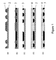
- the patterned conducting layer or stack of layers can be formed by electroplating. This is illustrated in Figs. 1.a to 1.c.
- a photoresist is applied on a uniform sacrificial metal layer (e.g. a Cu flexible foil) and patterned e.g. by photolithography (Fig. 1.a).
- photolithography e.g. a photolithography
- a directly printed resist can be used applied by stencil or screen printing, or flexo, gravure or offset printing. Any material which can be removed after applying the conducting layers can be used.
- a metal or metal stack e.g. Au/Ni/Cu
- conducting layer or stack of layers is electroplated onto the exposed metal (pattern plating) (Fig. 1.b).
- pattern plating e.g. Pt, Al, Ag, Au/Ni/Cu/Ni/Au, etc.
- photoresist is removed (Fig. 1.c).
- electroplating instead of electroplating other deposition techniques can be used, e,g, sputtering, thermal and e-gun evaporation, electroless (also called chemical) plating.
- electroless (also called chemical) plating e.g. sputtering, thermal and e-gun evaporation
- Several of these deposition techniques can also be used on insulating substrates. Patterning of these layers can be done in different ways for example by lift-off techniques or by patterning the layer using lithography and dry and/or wet etching techniques.
- the patterned conducting layer or stack of layers comprises a metal or a semiconductor material.
- Such conducting layers can serve well for electrical conduction. Electrical conduction can be used for interconnect purposes.
- the patterned conducting layer can be chosen such that it is optically conducting (ie conducting electromagnetic radiation as light) or thermally conducting (conducting heat).
- the flexible and/or stretchable material can then by applied on top and in between these patterned features. This can be done by spin coating or spinning, eventually followed by a curing step. Instead of spin coating also moulding techniques, curtain coating, dispensing or dipping can be used.
- the result is a stretchable substrate with embedded conductors. If flexible material is applied which is not stretchable the result will be a flexible substrate with embedded components (but not stretchable).
- a stretchable material e.g. silicone by spinning
- silicone any stretchable material can be used: latex, polyurethane, all kinds of rubbers like NBR (nitrile butadiene rubber), thermoplastic elestomers (TPE), TPEs are grouped into major families based on polyolefin (TPE-O), polyester (TPE-E), polyurethane (TPE-U), polyamide (TPE-A), and styrene(TPE-S).
- the soft stretchable material can also be a non-polar rubber, such as styrene butadiene rubber (SBR), ethylene propylene diene monomer (EPDM), or a polar rubber, such as nitrile butadiene rubber (NBR).
- SBR styrene butadiene rubber
- EPDM ethylene propylene diene monomer
- NBR nitrile butadiene rubber
- stretchable materials instead of stretchable materials also flexible materials like polyimide can be applied, resulting in a flexible circuit instead of a stretchable circuit.
- the patterned features can have a shape such that they are anchored into the stretchable or flexible material, which is a big advantage in flexible and especially stretchable electronics. Examples of shapes of the patterned features are given in Figure 3. Anchoring of the features into the stretchable and/or flexible material is achieved in Figures 3.b, 3.d, 3.e, and 3.f. If not anchored, or taken care of by possibly other means, said features may come loose from the composite substrate. Fig. 3c may have a lesser degree of adhesion, which may be solved by other means as for instance by choosing the right material combination - flexible and/or stretchable material and the patterned conducting layer material. Anchor structures may be provided in order to provide a good adhesion to the flexible and/or stretchable material film.
- the patterned features have a substantially trapezoidal shape.
- An ideal trapezoidal shape has 2 sides of equal length, and a top side and a bottom side.
- the top side is wider then the bottom side, such that flexible and/or stretchable material holds the features into place (see Fig. 3 b).
- the patterned features have sloped sidewalls.
- Trapezoidal shape or sloped sidewalls can be achieved by choosing the appropriate shape of the photoresist patterns after development.
- the developed photoresist preferably has sloped walls (number (1) in Fig. 1.a). This would result in conductors with trapezium-like cross sections (number (3) in Figs. 1.b and 1.c), enhancing the mechanical stability of the conductors, even under stretch, because the conductors are "plugged” in the stretchable material (number (3) in Fig 1.e).
- the sloped walls can easily be obtained using a positive photoresist.
- a suitable thick positive resist can be e.g. ma-P 1275 of Microresist (Berlin). However to obtain as fine pitches as possible, also resist patterning with vertical walls can be used. In this case the well known and widely used SU-8 negative resist from MicroChem is a suitable alternative for the positive resists.
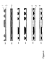
- FIG. 4. Patterning of the conductor is illustrated in Figures 4.a, 4.b, and 4.c.
- the sacrificial layer is partially etched with underetch or undercut underneath the patterned conductor (see Fig. 4.d).
- this material will fill the gap underneath the patterned conductor (Fig. 4.e).
- the sacrificial substrate is removed (Fig. 4.f)
- the patterned conductor is anchored into the stretchable and/or flexible material.
- a combination of the two previous methods for anchoring the conductor i.e. a combination of sloped sidewalls and extra etch step, results in even more reliable anchoring into the stretchable and/or flexible material.
- the present invention can have advantages in the field of production of fine pitch flex substrates. For instance a pitch of 40 ⁇ m for a Cu thickness of 4 ⁇ m, equivalent to a resistivity of 5m ⁇ /square, can be achieved.
- the proposed process offers the possibility for reel-to-reel implementation, so that it is potentially a cost competitive process, especially compared to some prior art processes, some of which for instance start from a Si wafer as the base substrate. A lot of prior art processes cannot be done in a reel-to-reel environment.
- Reel-to-reel is term known by a person of ordinary skill.
- R2R is a process where the starting substrate (in our case the sacrificial layer) under the format of a long tape is wound off a first reel, then is sent through all processing machines, and at the end of the processing the resulting product (in this case the stretchable substrate with embedded conductors) is wound back onto a second reel.
- the whole system can be compared with a tape recorder.
- Embodiments of the present invention have also some significant advantages, when it comes to embedding and assembly of components, e.g. ICs.
- An example of processing steps according this embodiment may comprise the following steps (see Figure 5):
- a metal stack is grown by pattern plating on a conductive sacrificial metal layer (Figure 5.a). Assembly of components at this stage of the substrate fabrication can be done, resulting in the situation illustrated in Figure 5.b. Such component can be placed on top, typically in electrical but optionally in optical contact with the patterned features. These patterned features can form an interconnect section. This has the enormous advantage that assembly is done on flexible, but not yet stretchable substrates. In this way complex components like very thin flip-chips can be assembled.
- an underfill material it can be necessary to apply an underfill material.
- the application of an underfill material may be advantageous in certain embodiments of the present invention, where the application of the stretchable and/or flexible material is not performing the underfill on itself.
- the underfill material is applied in substantially the whole area confined by the patterned features, the sacrificial layer and the respective component (number (7) in Figure 5.b). In other words such underfill may be applied in between the components and the sacrificial layer on substantially the overlap area of both.
- Suitable underfill materials or adhesives have to be provided, which are not attacked during the removal etch of the sacrificial layer.
- local stiffeners which might be flexible or even rigid
- Components can be used for locally strengthening the flexible device, or for controlling the areas of higher and lower flexibility requirements (number (8) in Figure 5.c).
- Such a component can be active or a passive. It can be rigid or flexible.
- Local limitation of substrate flexibility or stretchability can also be achieved by locally increasing the thickness of the applied flexible or stretchable material (number (9) in Figure 5.c). This locally thicker substrate has the same function as the local stiffener (number (8) in Figure 5.c).
- This local thickness increase can be achieved by using moulding techniques for the application of the flexible or stretchable materials, instead of curtain coating, dispensing, dipping or spincoating. These zones will deform less than the zones with thinner substrate material when the circuit is stretched, so the component connections will be subjected to smaller mechanical stresses.
- a component can be placed on the composite substrate, typically in electrical but optionally in optical contact with the patterned features, on the side where the sacrificial layer was removed. It is clear however that now the assembly takes place on a stretchable circuit. Another layer of stretchable and/or flexible material can be applied on top of such component, for certain applications. After introducing a second layer of components at the backside of the substrate (where the sacrificial layer is removed), the backside of the substrate in turn can be covered with the same or another second stretchable and/or flexible material, thus giving the possibility to also embed components, mounted on this backside ( Figure 5.f).
- This surface treatment may comprise a plasma treatment of the surface where the sacrificial layer is removed.
Landscapes
- Engineering & Computer Science (AREA)
- Manufacturing & Machinery (AREA)
- Microelectronics & Electronic Packaging (AREA)
- Structure Of Printed Boards (AREA)
- Laminated Bodies (AREA)
- Conductive Materials (AREA)
- Silicon Polymers (AREA)
- Manufacture Of Alloys Or Alloy Compounds (AREA)
Applications Claiming Priority (1)
| Application Number | Priority Date | Filing Date | Title |
|---|---|---|---|
| GBGB0505826.8A GB0505826D0 (en) | 2005-03-22 | 2005-03-22 | Methods for embedding of conducting material and devices resulting from said methods |
Publications (2)
| Publication Number | Publication Date |
|---|---|
| EP1746869A1 true EP1746869A1 (de) | 2007-01-24 |
| EP1746869B1 EP1746869B1 (de) | 2011-07-27 |
Family
ID=34531644
Family Applications (1)
| Application Number | Title | Priority Date | Filing Date |
|---|---|---|---|
| EP06005244A Expired - Lifetime EP1746869B1 (de) | 2005-03-22 | 2006-03-15 | Verfahren zum Einbetten von leitendem Material und danach hergestellte Vorrichtungen |
Country Status (4)
| Country | Link |
|---|---|
| US (2) | US7487587B2 (de) |
| EP (1) | EP1746869B1 (de) |
| AT (1) | ATE518411T1 (de) |
| GB (1) | GB0505826D0 (de) |
Cited By (4)
| Publication number | Priority date | Publication date | Assignee | Title |
|---|---|---|---|---|
| EP2355144A1 (de) | 2010-02-09 | 2011-08-10 | Nederlandse Organisatie voor toegepast -natuurwetenschappelijk onderzoek TNO | Bestückung auf flexiblen und/oder dehnbaren Substraten |
| US9338894B2 (en) | 2010-12-03 | 2016-05-10 | Nederlandse Organisatie Voor Toegepast-Natuurwetenschappelijk Onderzoek Tno | Method and apparatus for assembling electric components on a flexible substrate as well as assembly of an electric component with a flexible substrate |
| US9723122B2 (en) | 2009-10-01 | 2017-08-01 | Mc10, Inc. | Protective cases with integrated electronics |
| US10204855B2 (en) | 2014-07-11 | 2019-02-12 | Intel Corporation | Bendable and stretchable electronic devices and methods |
Families Citing this family (70)
| Publication number | Priority date | Publication date | Assignee | Title |
|---|---|---|---|---|
| JP4902248B2 (ja) * | 2006-04-07 | 2012-03-21 | 株式会社日本マイクロニクス | 電気的接続装置 |
| JP4884821B2 (ja) * | 2006-04-14 | 2012-02-29 | 株式会社日本マイクロニクス | プローブシートおよび電気的接続装置 |
| JP4841298B2 (ja) * | 2006-04-14 | 2011-12-21 | 株式会社日本マイクロニクス | プローブシートの製造方法 |
| JP2008082912A (ja) * | 2006-09-28 | 2008-04-10 | Micronics Japan Co Ltd | 電気的接続装置 |
| DE102006055576A1 (de) * | 2006-11-21 | 2008-05-29 | Fraunhofer-Gesellschaft zur Förderung der angewandten Forschung e.V. | Verfahren zum Herstellen eines dehnbaren Schaltungsträgers und dehnbarer Schaltungsträger |
| TWI723953B (zh) * | 2008-03-05 | 2021-04-11 | 美國伊利諾大學理事會 | 可延展且可折疊的電子裝置 |
| US8207473B2 (en) * | 2008-06-24 | 2012-06-26 | Imec | Method for manufacturing a stretchable electronic device |
| US8886334B2 (en) | 2008-10-07 | 2014-11-11 | Mc10, Inc. | Systems, methods, and devices using stretchable or flexible electronics for medical applications |
| US9123614B2 (en) | 2008-10-07 | 2015-09-01 | Mc10, Inc. | Methods and applications of non-planar imaging arrays |
| US8372726B2 (en) | 2008-10-07 | 2013-02-12 | Mc10, Inc. | Methods and applications of non-planar imaging arrays |
| US8389862B2 (en) | 2008-10-07 | 2013-03-05 | Mc10, Inc. | Extremely stretchable electronics |
| US9545216B2 (en) | 2011-08-05 | 2017-01-17 | Mc10, Inc. | Catheter balloon methods and apparatus employing sensing elements |
| US8097926B2 (en) | 2008-10-07 | 2012-01-17 | Mc10, Inc. | Systems, methods, and devices having stretchable integrated circuitry for sensing and delivering therapy |
| US9119533B2 (en) | 2008-10-07 | 2015-09-01 | Mc10, Inc. | Systems, methods, and devices having stretchable integrated circuitry for sensing and delivering therapy |
| US9289132B2 (en) | 2008-10-07 | 2016-03-22 | Mc10, Inc. | Catheter balloon having stretchable integrated circuitry and sensor array |
| WO2010086033A1 (en) | 2009-01-30 | 2010-08-05 | Interuniversitair Microelektronica Centrum Vzw | Stretchable electronic device |
| WO2010086416A1 (en) | 2009-01-30 | 2010-08-05 | Imec | Stretchable electronic device |
| JP4944145B2 (ja) * | 2009-03-19 | 2012-05-30 | 太陽誘電株式会社 | 圧電薄膜共振子、フィルタ、通信モジュール、通信装置 |
| WO2011008459A2 (en) * | 2009-06-29 | 2011-01-20 | Infinite Corridor Technology, Llc | Structured material substrates for flexible, stretchable electronics |
| US20110218756A1 (en) * | 2009-10-01 | 2011-09-08 | Mc10, Inc. | Methods and apparatus for conformal sensing of force and/or acceleration at a person's head |
| TWI419278B (zh) * | 2010-10-26 | 2013-12-11 | 欣興電子股份有限公司 | 封裝基板及其製法 |
| WO2012125494A2 (en) | 2011-03-11 | 2012-09-20 | Mc10, Inc. | Integrated devices to facilitate quantitative assays and diagnostics |
| WO2012166686A2 (en) | 2011-05-27 | 2012-12-06 | Mc10, Inc. | Electronic, optical and/or mechanical apparatus and systems and methods for fabricating same |
| FR2975985B1 (fr) * | 2011-05-30 | 2016-02-12 | Univ Paris Sud 11 | Procede pour la realisation de supports fonctionnels souples. |
| US9757050B2 (en) | 2011-08-05 | 2017-09-12 | Mc10, Inc. | Catheter balloon employing force sensing elements |
| EP2786131B1 (de) | 2011-09-01 | 2018-11-07 | Mc10, Inc. | Elektronik zur erfassung des zustandes von gewebe |
| DE112012004146T5 (de) | 2011-10-05 | 2014-11-06 | Mc10, Inc. | Herzkatheter mit Verwendung oberflächentreuer Elektronik zur Abbildung |
| US9121106B2 (en) * | 2012-02-28 | 2015-09-01 | Texas Instruments Incorporated | Method of forming a laminated magnetic core with sputter deposited and electroplated layers |
| US9947609B2 (en) | 2012-03-09 | 2018-04-17 | Honeywell International Inc. | Integrated circuit stack |
| US9226402B2 (en) | 2012-06-11 | 2015-12-29 | Mc10, Inc. | Strain isolation structures for stretchable electronics |
| US9247637B2 (en) | 2012-06-11 | 2016-01-26 | Mc10, Inc. | Strain relief structures for stretchable interconnects |
| US9295842B2 (en) | 2012-07-05 | 2016-03-29 | Mc10, Inc. | Catheter or guidewire device including flow sensing and use thereof |
| JP2015521894A (ja) | 2012-07-05 | 2015-08-03 | エムシー10 インコーポレイテッドMc10,Inc. | 流量センシングを含むカテーテルデバイス |
| CN105008949A (zh) | 2012-10-09 | 2015-10-28 | Mc10股份有限公司 | 与服装整合的保形电子装置 |
| US9171794B2 (en) | 2012-10-09 | 2015-10-27 | Mc10, Inc. | Embedding thin chips in polymer |
| US9706647B2 (en) | 2013-05-14 | 2017-07-11 | Mc10, Inc. | Conformal electronics including nested serpentine interconnects |
| KR20160040670A (ko) | 2013-08-05 | 2016-04-14 | 엠씨10, 인크 | 곡면부착형 전자기기를 포함하는 유연한 온도 센서 |
| US10467926B2 (en) | 2013-10-07 | 2019-11-05 | Mc10, Inc. | Conformal sensor systems for sensing and analysis |
| JP6711750B2 (ja) | 2013-11-22 | 2020-06-17 | エムシー10 インコーポレイテッドMc10,Inc. | 心臓活動の検知および分析のためのコンフォーマルセンサシステム |
| WO2015103580A2 (en) | 2014-01-06 | 2015-07-09 | Mc10, Inc. | Encapsulated conformal electronic systems and devices, and methods of making and using the same |
| KR20160129007A (ko) | 2014-03-04 | 2016-11-08 | 엠씨10, 인크 | 전자 디바이스를 위한 다부분 유연성 봉지 하우징 |
| JP6661242B2 (ja) | 2014-03-12 | 2020-03-11 | エムシー10 インコーポレイテッドMc10,Inc. | アッセイの変化の定量化のための測定装置および方法 |
| US10103037B2 (en) | 2014-05-09 | 2018-10-16 | Intel Corporation | Flexible microelectronic systems and methods of fabricating the same |
| KR101924560B1 (ko) | 2014-09-29 | 2019-02-27 | 엘지디스플레이 주식회사 | 벤딩 스트레스를 감소시키는 와이어들을 구비한 플렉서블 디스플레이 장치 |
| US9899330B2 (en) | 2014-10-03 | 2018-02-20 | Mc10, Inc. | Flexible electronic circuits with embedded integrated circuit die |
| US10297572B2 (en) | 2014-10-06 | 2019-05-21 | Mc10, Inc. | Discrete flexible interconnects for modules of integrated circuits |
| USD781270S1 (en) | 2014-10-15 | 2017-03-14 | Mc10, Inc. | Electronic device having antenna |
| EP3258837A4 (de) | 2015-02-20 | 2018-10-10 | Mc10, Inc. | Automatische erkennung und konfiguration von am körper tragbaren vorrichtungen auf basis von status, position und/oder ausrichtung am körper |
| US10398343B2 (en) | 2015-03-02 | 2019-09-03 | Mc10, Inc. | Perspiration sensor |
| US9548277B2 (en) | 2015-04-21 | 2017-01-17 | Honeywell International Inc. | Integrated circuit stack including a patterned array of electrically conductive pillars |
| JP6484133B2 (ja) * | 2015-07-09 | 2019-03-13 | 日東電工株式会社 | 配線回路基板の製造方法 |
| JP6491556B2 (ja) * | 2015-07-09 | 2019-03-27 | 日東電工株式会社 | 配線回路基板 |
| US10653332B2 (en) | 2015-07-17 | 2020-05-19 | Mc10, Inc. | Conductive stiffener, method of making a conductive stiffener, and conductive adhesive and encapsulation layers |
| US10709384B2 (en) | 2015-08-19 | 2020-07-14 | Mc10, Inc. | Wearable heat flux devices and methods of use |
| CN108290070A (zh) | 2015-10-01 | 2018-07-17 | Mc10股份有限公司 | 用于与虚拟环境相互作用的方法和系统 |
| WO2017062508A1 (en) | 2015-10-05 | 2017-04-13 | Mc10, Inc. | Method and System for Neuromodulation and Stimulation |
| TWI587763B (zh) * | 2015-11-17 | 2017-06-11 | The use of gravure printing method to form conductive totem | |
| US10080290B2 (en) * | 2015-11-17 | 2018-09-18 | Intel Corporation | Stretchable embedded electronic package |
| CN108781313B (zh) | 2016-02-22 | 2022-04-08 | 美谛达解决方案公司 | 用以贴身获取传感器信息的耦接的集线器和传感器节点的系统、装置和方法 |
| EP3420732B8 (de) | 2016-02-22 | 2020-12-30 | Medidata Solutions, Inc. | System, vorrichtungen und verfahren zur daten- und leistungsübertragung auf dem körper |
| US10076025B2 (en) * | 2016-02-22 | 2018-09-11 | Nippon Mektron, Ltd. | Stretchable circuit board and method for manufacturing the same |
| CN109310340A (zh) | 2016-04-19 | 2019-02-05 | Mc10股份有限公司 | 用于测量汗液的方法和系统 |
| US10447347B2 (en) | 2016-08-12 | 2019-10-15 | Mc10, Inc. | Wireless charger and high speed data off-loader |
| EP3322267B1 (de) * | 2016-11-10 | 2025-02-19 | AT & S Austria Technologie & Systemtechnik Aktiengesellschaft | Komponententräger mit haftfördernder form von verdrahtungsstruktur |
| CN108156763B (zh) * | 2016-12-05 | 2020-08-07 | 鹏鼎控股(深圳)股份有限公司 | 透明电路板及其制作方法 |
| CN108401361B (zh) * | 2017-02-04 | 2020-08-07 | 欣兴电子股份有限公司 | 电路板与其制作方法 |
| US10512165B2 (en) | 2017-03-23 | 2019-12-17 | Unimicron Technology Corp. | Method for manufacturing a circuit board |
| FR3083918B1 (fr) * | 2018-07-13 | 2020-10-23 | Commissariat Energie Atomique | Procede de transfert de structures |
| US11749455B2 (en) * | 2022-01-10 | 2023-09-05 | Bh Electronics, Inc. | Methods of fabricating ultra-miniature laminated magnetic cores and devices |
| CN118748864B (zh) * | 2024-08-13 | 2025-01-17 | 哈尔滨工业大学(深圳)(哈尔滨工业大学深圳科技创新研究院) | 可拉伸电路及其制备方法、柔性电子集成系统 |
Citations (5)
| Publication number | Priority date | Publication date | Assignee | Title |
|---|---|---|---|---|
| US3279969A (en) | 1962-11-29 | 1966-10-18 | Amphenol Corp | Method of making electronic circuit elements |
| US4584039A (en) * | 1984-12-26 | 1986-04-22 | Hughes Aircraft Co. | Fine line flexible cable fabrication process |
| US5147519A (en) * | 1990-07-27 | 1992-09-15 | Motorola, Inc. | Method of manufacturing elastomers containing fine line conductors |
| EP0545328A2 (de) | 1991-11-29 | 1993-06-09 | Hitachi Chemical Co., Ltd. | Herstellungsverfahren für eine gedruckte Schaltung |
| US20020192439A1 (en) * | 2001-06-14 | 2002-12-19 | International Business Machines Corporation | Structure having embedded flush circuitry features and method of fabricating |
Family Cites Families (11)
| Publication number | Priority date | Publication date | Assignee | Title |
|---|---|---|---|---|
| ES2063151T3 (es) * | 1988-03-30 | 1995-01-01 | Rhone Poulenc Chimie | Procedimiento de preparacion de oxido de titanio. |
| US5436412A (en) * | 1992-10-30 | 1995-07-25 | International Business Machines Corporation | Interconnect structure having improved metallization |
| DE19617055C1 (de) * | 1996-04-29 | 1997-06-26 | Semikron Elektronik Gmbh | Halbleiterleistungsmodul hoher Packungsdichte in Mehrschichtbauweise |
| JP4066522B2 (ja) * | 1998-07-22 | 2008-03-26 | イビデン株式会社 | プリント配線板 |
| JP3935309B2 (ja) * | 2000-06-08 | 2007-06-20 | 日東電工株式会社 | 配線回路基板およびその製造方法 |
| JP4459406B2 (ja) * | 2000-07-27 | 2010-04-28 | ソニーケミカル&インフォメーションデバイス株式会社 | フレキシブル配線板製造方法 |
| US7491892B2 (en) * | 2003-03-28 | 2009-02-17 | Princeton University | Stretchable and elastic interconnects |
| US7337012B2 (en) * | 2003-04-30 | 2008-02-26 | Lawrence Livermore National Security, Llc | Stretchable polymer-based electronic device |
| US7056759B2 (en) * | 2004-04-27 | 2006-06-06 | Hewlett-Packard Development Company, L.P. | Method for making a microelectromechanical system using a flexure protection layer |
| KR100643756B1 (ko) * | 2004-09-10 | 2006-11-10 | 삼성전자주식회사 | 유연소자, 유연압력센서, 및 이들의 제조방법 |
| TWI370714B (en) * | 2008-01-09 | 2012-08-11 | Ind Tech Res Inst | Circuit structure and menufacturing method thereof |
-
2005
- 2005-03-22 GB GBGB0505826.8A patent/GB0505826D0/en not_active Ceased
-
2006
- 2006-03-15 EP EP06005244A patent/EP1746869B1/de not_active Expired - Lifetime
- 2006-03-15 AT AT06005244T patent/ATE518411T1/de not_active IP Right Cessation
- 2006-03-22 US US11/387,446 patent/US7487587B2/en active Active
-
2009
- 2009-01-05 US US12/348,814 patent/US8431828B2/en not_active Expired - Fee Related
Patent Citations (5)
| Publication number | Priority date | Publication date | Assignee | Title |
|---|---|---|---|---|
| US3279969A (en) | 1962-11-29 | 1966-10-18 | Amphenol Corp | Method of making electronic circuit elements |
| US4584039A (en) * | 1984-12-26 | 1986-04-22 | Hughes Aircraft Co. | Fine line flexible cable fabrication process |
| US5147519A (en) * | 1990-07-27 | 1992-09-15 | Motorola, Inc. | Method of manufacturing elastomers containing fine line conductors |
| EP0545328A2 (de) | 1991-11-29 | 1993-06-09 | Hitachi Chemical Co., Ltd. | Herstellungsverfahren für eine gedruckte Schaltung |
| US20020192439A1 (en) * | 2001-06-14 | 2002-12-19 | International Business Machines Corporation | Structure having embedded flush circuitry features and method of fabricating |
Cited By (9)
| Publication number | Priority date | Publication date | Assignee | Title |
|---|---|---|---|---|
| US9723122B2 (en) | 2009-10-01 | 2017-08-01 | Mc10, Inc. | Protective cases with integrated electronics |
| EP2355144A1 (de) | 2010-02-09 | 2011-08-10 | Nederlandse Organisatie voor toegepast -natuurwetenschappelijk onderzoek TNO | Bestückung auf flexiblen und/oder dehnbaren Substraten |
| WO2011099851A1 (en) | 2010-02-09 | 2011-08-18 | Nederlandse Organisatie Voor Toegepast-Natuurwetenschappelijk Onderzoek Tno | Component placement on flexible and/or stretchable substrates |
| CN102822960A (zh) * | 2010-02-09 | 2012-12-12 | 荷兰应用自然科学研究组织Tno | 柔性和/或可伸缩的衬底上的组件布局 |
| JP2013519242A (ja) * | 2010-02-09 | 2013-05-23 | ネーデルランゼ オルハニサティー フォール トゥーヘパスト−ナトゥールウェテンスハッペァイク オンデルゾーク テーエンオー | フレキシブル基板及び/又は伸長可能な基板上の部品配置 |
| US8961725B2 (en) | 2010-02-09 | 2015-02-24 | Nederlandse Organisatie Voor Toegepast-Natuurwetenschappelijk Onderzoek Tno | Component placement on flexible and/or stretchable substrates |
| CN102822960B (zh) * | 2010-02-09 | 2015-06-10 | 荷兰应用自然科学研究组织Tno | 柔性和/或可伸缩的衬底上的组件布局 |
| US9338894B2 (en) | 2010-12-03 | 2016-05-10 | Nederlandse Organisatie Voor Toegepast-Natuurwetenschappelijk Onderzoek Tno | Method and apparatus for assembling electric components on a flexible substrate as well as assembly of an electric component with a flexible substrate |
| US10204855B2 (en) | 2014-07-11 | 2019-02-12 | Intel Corporation | Bendable and stretchable electronic devices and methods |
Also Published As
| Publication number | Publication date |
|---|---|
| US7487587B2 (en) | 2009-02-10 |
| US20060231288A1 (en) | 2006-10-19 |
| EP1746869B1 (de) | 2011-07-27 |
| GB0505826D0 (en) | 2005-04-27 |
| US20090107704A1 (en) | 2009-04-30 |
| ATE518411T1 (de) | 2011-08-15 |
| US8431828B2 (en) | 2013-04-30 |
Similar Documents
| Publication | Publication Date | Title |
|---|---|---|
| EP1746869B1 (de) | Verfahren zum Einbetten von leitendem Material und danach hergestellte Vorrichtungen | |
| US6528350B2 (en) | Method for fabricating a metal plated spring structure | |
| US8383958B2 (en) | Method to build robust mechanical structures on substrate surfaces | |
| US6684499B2 (en) | Method for fabricating a spring structure | |
| JP5139432B2 (ja) | カーボンナノチューブ・コンタクト構造 | |
| EP1277696A2 (de) | Feder mit leitfähiger Beschichtung | |
| EP0192349A2 (de) | Verfahren zum Einbetten von Leitern in Polyimid | |
| WO2010086033A1 (en) | Stretchable electronic device | |
| EP1304768B1 (de) | Federstruktur | |
| US20150084089A1 (en) | Insulation structure for high temperature conditions and manufacturing method thereof | |
| US20090101513A1 (en) | Method of manufacturing a film printed circuit board | |
| KR20080090285A (ko) | 배선 기판 및 그 제조 방법 | |
| KR100934107B1 (ko) | 미세 피치의 금속 범프를 제공하는 인쇄회로기판 제조 방법 | |
| EP0836228A2 (de) | Verbessertes Trägerband | |
| JP2000299339A (ja) | 半導体装置の製造方法 | |
| JP2003218151A (ja) | 無電解メッキバンプの形成方法、半導体装置及びその製造方法 | |
| JP4077666B2 (ja) | コンタクトプローブの製造方法 | |
| JP2004087862A (ja) | 半導体装置用テープキャリア | |
| JP3699294B2 (ja) | プリント配線板の製造方法 | |
| KR100447495B1 (ko) | 테이프캐리어형 반도체패키지의 배선패턴 및 이의 제조방법 | |
| CN1942056A (zh) | 柔性电路板的制造方法 | |
| JP2001127062A (ja) | 配線の形成方法 | |
| JP2004072027A (ja) | 突起電極付き配線基板の製造方法 | |
| JP2004207262A (ja) | 薄膜多層回路基板及びその製造方法 | |
| JPH0677650A (ja) | 多層配線板の製造方法 |
Legal Events
| Date | Code | Title | Description |
|---|---|---|---|
| PUAI | Public reference made under article 153(3) epc to a published international application that has entered the european phase |
Free format text: ORIGINAL CODE: 0009012 |
|
| AK | Designated contracting states |
Kind code of ref document: A1 Designated state(s): AT BE BG CH CY CZ DE DK EE ES FI FR GB GR HU IE IS IT LI LT LU LV MC NL PL PT RO SE SI SK TR |
|
| AX | Request for extension of the european patent |
Extension state: AL BA HR MK YU |
|
| 17P | Request for examination filed |
Effective date: 20070724 |
|
| 17Q | First examination report despatched |
Effective date: 20070823 |
|
| AKX | Designation fees paid |
Designated state(s): AT BE BG CH CY CZ DE DK EE ES FI FR GB GR HU IE IS IT LI LT LU LV MC NL PL PT RO SE SI SK TR |
|
| RAP1 | Party data changed (applicant data changed or rights of an application transferred) |
Owner name: IMEC Owner name: UNIVERSITEIT GENT |
|
| GRAP | Despatch of communication of intention to grant a patent |
Free format text: ORIGINAL CODE: EPIDOSNIGR1 |
|
| GRAS | Grant fee paid |
Free format text: ORIGINAL CODE: EPIDOSNIGR3 |
|
| GRAA | (expected) grant |
Free format text: ORIGINAL CODE: 0009210 |
|
| AK | Designated contracting states |
Kind code of ref document: B1 Designated state(s): AT BE BG CH CY CZ DE DK EE ES FI FR GB GR HU IE IS IT LI LT LU LV MC NL PL PT RO SE SI SK TR |
|
| REG | Reference to a national code |
Ref country code: GB Ref legal event code: FG4D |
|
| REG | Reference to a national code |
Ref country code: CH Ref legal event code: EP |
|
| REG | Reference to a national code |
Ref country code: DE Ref legal event code: R096 Ref document number: 602006023248 Country of ref document: DE Effective date: 20110915 |
|
| REG | Reference to a national code |
Ref country code: NL Ref legal event code: VDEP Effective date: 20110727 |
|
| REG | Reference to a national code |
Ref country code: AT Ref legal event code: MK05 Ref document number: 518411 Country of ref document: AT Kind code of ref document: T Effective date: 20110727 |
|
| PG25 | Lapsed in a contracting state [announced via postgrant information from national office to epo] |
Ref country code: NL Free format text: LAPSE BECAUSE OF FAILURE TO SUBMIT A TRANSLATION OF THE DESCRIPTION OR TO PAY THE FEE WITHIN THE PRESCRIBED TIME-LIMIT Effective date: 20110727 Ref country code: SE Free format text: LAPSE BECAUSE OF FAILURE TO SUBMIT A TRANSLATION OF THE DESCRIPTION OR TO PAY THE FEE WITHIN THE PRESCRIBED TIME-LIMIT Effective date: 20110727 Ref country code: LT Free format text: LAPSE BECAUSE OF FAILURE TO SUBMIT A TRANSLATION OF THE DESCRIPTION OR TO PAY THE FEE WITHIN THE PRESCRIBED TIME-LIMIT Effective date: 20110727 Ref country code: IS Free format text: LAPSE BECAUSE OF FAILURE TO SUBMIT A TRANSLATION OF THE DESCRIPTION OR TO PAY THE FEE WITHIN THE PRESCRIBED TIME-LIMIT Effective date: 20111127 Ref country code: FI Free format text: LAPSE BECAUSE OF FAILURE TO SUBMIT A TRANSLATION OF THE DESCRIPTION OR TO PAY THE FEE WITHIN THE PRESCRIBED TIME-LIMIT Effective date: 20110727 Ref country code: PT Free format text: LAPSE BECAUSE OF FAILURE TO SUBMIT A TRANSLATION OF THE DESCRIPTION OR TO PAY THE FEE WITHIN THE PRESCRIBED TIME-LIMIT Effective date: 20111128 |
|
| PG25 | Lapsed in a contracting state [announced via postgrant information from national office to epo] |
Ref country code: LV Free format text: LAPSE BECAUSE OF FAILURE TO SUBMIT A TRANSLATION OF THE DESCRIPTION OR TO PAY THE FEE WITHIN THE PRESCRIBED TIME-LIMIT Effective date: 20110727 Ref country code: GR Free format text: LAPSE BECAUSE OF FAILURE TO SUBMIT A TRANSLATION OF THE DESCRIPTION OR TO PAY THE FEE WITHIN THE PRESCRIBED TIME-LIMIT Effective date: 20111028 Ref country code: SI Free format text: LAPSE BECAUSE OF FAILURE TO SUBMIT A TRANSLATION OF THE DESCRIPTION OR TO PAY THE FEE WITHIN THE PRESCRIBED TIME-LIMIT Effective date: 20110727 Ref country code: CY Free format text: LAPSE BECAUSE OF FAILURE TO SUBMIT A TRANSLATION OF THE DESCRIPTION OR TO PAY THE FEE WITHIN THE PRESCRIBED TIME-LIMIT Effective date: 20110727 Ref country code: AT Free format text: LAPSE BECAUSE OF FAILURE TO SUBMIT A TRANSLATION OF THE DESCRIPTION OR TO PAY THE FEE WITHIN THE PRESCRIBED TIME-LIMIT Effective date: 20110727 Ref country code: PL Free format text: LAPSE BECAUSE OF FAILURE TO SUBMIT A TRANSLATION OF THE DESCRIPTION OR TO PAY THE FEE WITHIN THE PRESCRIBED TIME-LIMIT Effective date: 20110727 |
|
| PG25 | Lapsed in a contracting state [announced via postgrant information from national office to epo] |
Ref country code: SK Free format text: LAPSE BECAUSE OF FAILURE TO SUBMIT A TRANSLATION OF THE DESCRIPTION OR TO PAY THE FEE WITHIN THE PRESCRIBED TIME-LIMIT Effective date: 20110727 Ref country code: CZ Free format text: LAPSE BECAUSE OF FAILURE TO SUBMIT A TRANSLATION OF THE DESCRIPTION OR TO PAY THE FEE WITHIN THE PRESCRIBED TIME-LIMIT Effective date: 20110727 |
|
| PG25 | Lapsed in a contracting state [announced via postgrant information from national office to epo] |
Ref country code: EE Free format text: LAPSE BECAUSE OF FAILURE TO SUBMIT A TRANSLATION OF THE DESCRIPTION OR TO PAY THE FEE WITHIN THE PRESCRIBED TIME-LIMIT Effective date: 20110727 Ref country code: RO Free format text: LAPSE BECAUSE OF FAILURE TO SUBMIT A TRANSLATION OF THE DESCRIPTION OR TO PAY THE FEE WITHIN THE PRESCRIBED TIME-LIMIT Effective date: 20110727 Ref country code: IT Free format text: LAPSE BECAUSE OF FAILURE TO SUBMIT A TRANSLATION OF THE DESCRIPTION OR TO PAY THE FEE WITHIN THE PRESCRIBED TIME-LIMIT Effective date: 20110727 |
|
| PLBE | No opposition filed within time limit |
Free format text: ORIGINAL CODE: 0009261 |
|
| STAA | Information on the status of an ep patent application or granted ep patent |
Free format text: STATUS: NO OPPOSITION FILED WITHIN TIME LIMIT |
|
| PG25 | Lapsed in a contracting state [announced via postgrant information from national office to epo] |
Ref country code: DK Free format text: LAPSE BECAUSE OF FAILURE TO SUBMIT A TRANSLATION OF THE DESCRIPTION OR TO PAY THE FEE WITHIN THE PRESCRIBED TIME-LIMIT Effective date: 20110727 |
|
| 26N | No opposition filed |
Effective date: 20120502 |
|
| REG | Reference to a national code |
Ref country code: DE Ref legal event code: R097 Ref document number: 602006023248 Country of ref document: DE Effective date: 20120502 |
|
| PG25 | Lapsed in a contracting state [announced via postgrant information from national office to epo] |
Ref country code: MC Free format text: LAPSE BECAUSE OF NON-PAYMENT OF DUE FEES Effective date: 20120331 |
|
| REG | Reference to a national code |
Ref country code: CH Ref legal event code: PL |
|
| REG | Reference to a national code |
Ref country code: IE Ref legal event code: MM4A |
|
| PG25 | Lapsed in a contracting state [announced via postgrant information from national office to epo] |
Ref country code: LI Free format text: LAPSE BECAUSE OF NON-PAYMENT OF DUE FEES Effective date: 20120331 Ref country code: CH Free format text: LAPSE BECAUSE OF NON-PAYMENT OF DUE FEES Effective date: 20120331 Ref country code: IE Free format text: LAPSE BECAUSE OF NON-PAYMENT OF DUE FEES Effective date: 20120315 |
|
| PG25 | Lapsed in a contracting state [announced via postgrant information from national office to epo] |
Ref country code: ES Free format text: LAPSE BECAUSE OF FAILURE TO SUBMIT A TRANSLATION OF THE DESCRIPTION OR TO PAY THE FEE WITHIN THE PRESCRIBED TIME-LIMIT Effective date: 20111107 |
|
| PG25 | Lapsed in a contracting state [announced via postgrant information from national office to epo] |
Ref country code: BG Free format text: LAPSE BECAUSE OF FAILURE TO SUBMIT A TRANSLATION OF THE DESCRIPTION OR TO PAY THE FEE WITHIN THE PRESCRIBED TIME-LIMIT Effective date: 20111027 |
|
| PG25 | Lapsed in a contracting state [announced via postgrant information from national office to epo] |
Ref country code: TR Free format text: LAPSE BECAUSE OF FAILURE TO SUBMIT A TRANSLATION OF THE DESCRIPTION OR TO PAY THE FEE WITHIN THE PRESCRIBED TIME-LIMIT Effective date: 20110727 |
|
| PG25 | Lapsed in a contracting state [announced via postgrant information from national office to epo] |
Ref country code: LU Free format text: LAPSE BECAUSE OF NON-PAYMENT OF DUE FEES Effective date: 20120315 |
|
| PG25 | Lapsed in a contracting state [announced via postgrant information from national office to epo] |
Ref country code: HU Free format text: LAPSE BECAUSE OF FAILURE TO SUBMIT A TRANSLATION OF THE DESCRIPTION OR TO PAY THE FEE WITHIN THE PRESCRIBED TIME-LIMIT Effective date: 20060315 |
|
| REG | Reference to a national code |
Ref country code: FR Ref legal event code: PLFP Year of fee payment: 11 |
|
| REG | Reference to a national code |
Ref country code: FR Ref legal event code: PLFP Year of fee payment: 12 |
|
| REG | Reference to a national code |
Ref country code: FR Ref legal event code: PLFP Year of fee payment: 13 |
|
| PGFP | Annual fee paid to national office [announced via postgrant information from national office to epo] |
Ref country code: DE Payment date: 20200218 Year of fee payment: 15 Ref country code: GB Payment date: 20200221 Year of fee payment: 15 |
|
| PGFP | Annual fee paid to national office [announced via postgrant information from national office to epo] |
Ref country code: BE Payment date: 20200228 Year of fee payment: 15 |
|
| PGFP | Annual fee paid to national office [announced via postgrant information from national office to epo] |
Ref country code: FR Payment date: 20200220 Year of fee payment: 15 |
|
| REG | Reference to a national code |
Ref country code: DE Ref legal event code: R119 Ref document number: 602006023248 Country of ref document: DE |
|
| GBPC | Gb: european patent ceased through non-payment of renewal fee |
Effective date: 20210315 |
|
| REG | Reference to a national code |
Ref country code: BE Ref legal event code: MM Effective date: 20210331 |
|
| PG25 | Lapsed in a contracting state [announced via postgrant information from national office to epo] |
Ref country code: DE Free format text: LAPSE BECAUSE OF NON-PAYMENT OF DUE FEES Effective date: 20211001 Ref country code: FR Free format text: LAPSE BECAUSE OF NON-PAYMENT OF DUE FEES Effective date: 20210331 Ref country code: GB Free format text: LAPSE BECAUSE OF NON-PAYMENT OF DUE FEES Effective date: 20210315 |
|
| PG25 | Lapsed in a contracting state [announced via postgrant information from national office to epo] |
Ref country code: BE Free format text: LAPSE BECAUSE OF NON-PAYMENT OF DUE FEES Effective date: 20210331 |