EP1748030A2 - Verfahren und Apparat zur statistischen Charakterisierung von Nano-Partikeln - Google Patents
Verfahren und Apparat zur statistischen Charakterisierung von Nano-Partikeln Download PDFInfo
- Publication number
- EP1748030A2 EP1748030A2 EP06116365A EP06116365A EP1748030A2 EP 1748030 A2 EP1748030 A2 EP 1748030A2 EP 06116365 A EP06116365 A EP 06116365A EP 06116365 A EP06116365 A EP 06116365A EP 1748030 A2 EP1748030 A2 EP 1748030A2
- Authority
- EP
- European Patent Office
- Prior art keywords
- nano
- particles
- pattern
- distributing
- measuring
- Prior art date
- Legal status (The legal status is an assumption and is not a legal conclusion. Google has not performed a legal analysis and makes no representation as to the accuracy of the status listed.)
- Granted
Links
Images


Classifications
-
- G—PHYSICS
- G01—MEASURING; TESTING
- G01N—INVESTIGATING OR ANALYSING MATERIALS BY DETERMINING THEIR CHEMICAL OR PHYSICAL PROPERTIES
- G01N15/00—Investigating characteristics of particles; Investigating permeability, pore-volume or surface-area of porous materials
- G01N15/02—Investigating particle size or size distribution
- G01N15/0205—Investigating particle size or size distribution by optical means
- G01N15/0227—Investigating particle size or size distribution by optical means using imaging; using holography
-
- B—PERFORMING OPERATIONS; TRANSPORTING
- B82—NANOTECHNOLOGY
- B82Y—SPECIFIC USES OR APPLICATIONS OF NANOSTRUCTURES; MEASUREMENT OR ANALYSIS OF NANOSTRUCTURES; MANUFACTURE OR TREATMENT OF NANOSTRUCTURES
- B82Y15/00—Nanotechnology for interacting, sensing or actuating, e.g. quantum dots as markers in protein assays or molecular motors
-
- B—PERFORMING OPERATIONS; TRANSPORTING
- B82—NANOTECHNOLOGY
- B82Y—SPECIFIC USES OR APPLICATIONS OF NANOSTRUCTURES; MEASUREMENT OR ANALYSIS OF NANOSTRUCTURES; MANUFACTURE OR TREATMENT OF NANOSTRUCTURES
- B82Y30/00—Nanotechnology for materials or surface science, e.g. nanocomposites
-
- G—PHYSICS
- G01—MEASURING; TESTING
- G01N—INVESTIGATING OR ANALYSING MATERIALS BY DETERMINING THEIR CHEMICAL OR PHYSICAL PROPERTIES
- G01N1/00—Sampling; Preparing specimens for investigation
- G01N1/28—Preparing specimens for investigation including physical details of (bio-)chemical methods covered elsewhere, e.g. G01N33/50, C12Q
- G01N1/40—Concentrating samples
- G01N2001/4038—Concentrating samples electric methods, e.g. electromigration, electrophoresis, ionisation
-
- G—PHYSICS
- G01—MEASURING; TESTING
- G01N—INVESTIGATING OR ANALYSING MATERIALS BY DETERMINING THEIR CHEMICAL OR PHYSICAL PROPERTIES
- G01N15/00—Investigating characteristics of particles; Investigating permeability, pore-volume or surface-area of porous materials
- G01N2015/0038—Investigating nanoparticles
-
- Y—GENERAL TAGGING OF NEW TECHNOLOGICAL DEVELOPMENTS; GENERAL TAGGING OF CROSS-SECTIONAL TECHNOLOGIES SPANNING OVER SEVERAL SECTIONS OF THE IPC; TECHNICAL SUBJECTS COVERED BY FORMER USPC CROSS-REFERENCE ART COLLECTIONS [XRACs] AND DIGESTS
- Y10—TECHNICAL SUBJECTS COVERED BY FORMER USPC
- Y10S—TECHNICAL SUBJECTS COVERED BY FORMER USPC CROSS-REFERENCE ART COLLECTIONS [XRACs] AND DIGESTS
- Y10S977/00—Nanotechnology
- Y10S977/84—Manufacture, treatment, or detection of nanostructure
-
- Y—GENERAL TAGGING OF NEW TECHNOLOGICAL DEVELOPMENTS; GENERAL TAGGING OF CROSS-SECTIONAL TECHNOLOGIES SPANNING OVER SEVERAL SECTIONS OF THE IPC; TECHNICAL SUBJECTS COVERED BY FORMER USPC CROSS-REFERENCE ART COLLECTIONS [XRACs] AND DIGESTS
- Y10—TECHNICAL SUBJECTS COVERED BY FORMER USPC
- Y10S—TECHNICAL SUBJECTS COVERED BY FORMER USPC CROSS-REFERENCE ART COLLECTIONS [XRACs] AND DIGESTS
- Y10S977/00—Nanotechnology
- Y10S977/84—Manufacture, treatment, or detection of nanostructure
- Y10S977/842—Manufacture, treatment, or detection of nanostructure for carbon nanotubes or fullerenes
-
- Y—GENERAL TAGGING OF NEW TECHNOLOGICAL DEVELOPMENTS; GENERAL TAGGING OF CROSS-SECTIONAL TECHNOLOGIES SPANNING OVER SEVERAL SECTIONS OF THE IPC; TECHNICAL SUBJECTS COVERED BY FORMER USPC CROSS-REFERENCE ART COLLECTIONS [XRACs] AND DIGESTS
- Y10—TECHNICAL SUBJECTS COVERED BY FORMER USPC
- Y10S—TECHNICAL SUBJECTS COVERED BY FORMER USPC CROSS-REFERENCE ART COLLECTIONS [XRACs] AND DIGESTS
- Y10S977/00—Nanotechnology
- Y10S977/84—Manufacture, treatment, or detection of nanostructure
- Y10S977/849—Manufacture, treatment, or detection of nanostructure with scanning probe
-
- Y—GENERAL TAGGING OF NEW TECHNOLOGICAL DEVELOPMENTS; GENERAL TAGGING OF CROSS-SECTIONAL TECHNOLOGIES SPANNING OVER SEVERAL SECTIONS OF THE IPC; TECHNICAL SUBJECTS COVERED BY FORMER USPC CROSS-REFERENCE ART COLLECTIONS [XRACs] AND DIGESTS
- Y10—TECHNICAL SUBJECTS COVERED BY FORMER USPC
- Y10S—TECHNICAL SUBJECTS COVERED BY FORMER USPC CROSS-REFERENCE ART COLLECTIONS [XRACs] AND DIGESTS
- Y10S977/00—Nanotechnology
- Y10S977/84—Manufacture, treatment, or detection of nanostructure
- Y10S977/88—Manufacture, treatment, or detection of nanostructure with arrangement, process, or apparatus for testing
-
- Y—GENERAL TAGGING OF NEW TECHNOLOGICAL DEVELOPMENTS; GENERAL TAGGING OF CROSS-SECTIONAL TECHNOLOGIES SPANNING OVER SEVERAL SECTIONS OF THE IPC; TECHNICAL SUBJECTS COVERED BY FORMER USPC CROSS-REFERENCE ART COLLECTIONS [XRACs] AND DIGESTS
- Y10—TECHNICAL SUBJECTS COVERED BY FORMER USPC
- Y10S—TECHNICAL SUBJECTS COVERED BY FORMER USPC CROSS-REFERENCE ART COLLECTIONS [XRACs] AND DIGESTS
- Y10S977/00—Nanotechnology
- Y10S977/84—Manufacture, treatment, or detection of nanostructure
- Y10S977/88—Manufacture, treatment, or detection of nanostructure with arrangement, process, or apparatus for testing
- Y10S977/881—Microscopy or spectroscopy, e.g. sem, tem
Definitions
- the present invention relates to measuring small particles, and in particular, to characterizing populations of nano-particles.
- Nano-particles particularly carbon structures
- Such carbon structures include, for example, carbon nano-tubes ("CNT”), and fullerenes, also known as “bucky balls,” such as C-60, C70, C76, and C84.
- CNT carbon nano-tubes
- bucky balls such as C-60, C70, C76, and C84.
- Nano-particles could be used as a component of a drug delivery system to deliver a drug, radiation, or other therapeutic agent to a targeted part of the body.
- the size of the nano-particles is critical. Because applications that use nano-particles typically use large quantities of nano-particles, it is important to be able to characterize large groups, that is, populations of nano-particles.
- An object of the invention is to provide a method and apparatus to statistically characterize populations of nano-particles.
- a number of particles as individuals or in small groups, are spread on a surface.
- the particles are then characterized by an analytical instrument.
- instruments can efficiently analyze multiple particles without having to manipulate individual particles.
- the surface is prepared by forming a pattern of electrical charges on the surface.
- the particles can be ionized and the particles are arrayed on the surface in a pattern determined by the charge pattern and the electrical properties, such as the net charge, on the nano-particles.
- the particles are then characterized, for example, using an instrument that measures individual particles, such an electron microscope, along with automated pattern recognition software, that can find and characterize the individual nano-particles.
- an instrument such as a scatterometer, that characterizes the nano-particles spread on the surface, without measuring individual particles.
- Another method uses projection illumination whereby a broad beam of electrons is applied to the particles, and the resulting secondary or backscatter electrons are focused onto a two dimensional electron sensor array. An image is reconstructed and then analyzed, thereby avoiding single scans of individual particles.
- FIG. 1 is a flow chart showing the steps of a preferred embodiment of the invention.
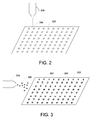
- FIG. 2 shows forming a charge pattern on a surface in accordance with a preferred embodiment of the invention.
- FIG. 3 shows nano-particles being sprayed over the charged distribution of FIG. 2.
- FIG. 4 shows the nano-particles of FIG. 3 being characterized by an electron microscope.
- FIG. 5 shows a statistical distribution of a characteristic of the nano-particles measured as shown in FIG. 4.
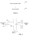
- FIG. 6 is flowchart showing preferred steps for ionizing nano-particles.
- FIG. 7 shows part of an apparatus for ionizing nano-particles and spraying the charged nano-particles onto a surface.
- a preferred embodiment spreads a large number of nano-particles onto a surface, and then characterizes the nano-particles to determine statistics describing the population. Because the particles are spread, it is easier to measure the particles and unnecessary to manipulate individual particles for measurement.
- the particles can be distributed by forming force centers on the surface, the force centers being areas that interact with the nano-particles to attract or repel them.
- the force centers can be, for example, groups of electrical charges that attract or repel ionized or polar nano-particles or chemicals that attract or repel the nano-particles or coatings on the nano-particles.
- the characterization of the particles could include, for example, dimensions, chemical composition, electrical properties, optical properties, or any other property. Any statistics could be determined from any of the properties. For example, the statistical distribution of a characteristic could be determined, including the mean, standard deviation, minimum, maximum, skew, kertosis, and other properties.
- the number of particles measured, either individually or as part of an overall measurement, to determine the statistics is typically greater than 25, greater than 50, greater than 100, or greater than 200. There is no upper limit to the number of nano-particles used in the characterization. Nano-particle, as the term is used herein, refers to particles that are smaller than 1000 ⁇ m, smaller than 100 ⁇ m, smaller than 10 ⁇ m, or smaller than 1 ⁇ m.
- the nano-particles are distributed in a deterministic pattern, that is, in a pattern determined by electrical charges or other force centers formed on a surface, to facilitate characterization.
- the nano-particles may be spread in a random pattern for characterization.
- the particles are aligned relative to each other or to a reference direction to facilitate ease or accuracy of measurement.
- carbon nano-tubes could be aligned so that the long dimension of individual particles are perpendicular to an electron microscope scan direction, with one end of all the individuals aligned to a reference line, thus facilitating measurement.
- the particles may be aligned by shaping the charge pattern, for example, by using continuous or discontinuous lines of charge, instead of dots of charge.
- the particles are distributed by ionizing the particles, forming a charge pattern on the surface, and then spraying the ionized particles onto the surface, with the charge pattern determining the distribution of the particles.
- the particles may not require an ionizing step.
- charged or uncharged particles can be randomly spread on the surface, without using a charge pattern.
- the repulsion among particles can be used to distribute the particles.
- dipole moments of the charges are used, instead of ionization.
- chemical or other forces are used to determine the nano-particles pattern.
- FIG. 1 shows the steps of a preferred embodiment.
- a charged pattern is formed on a substrate.
- FIG. 2 shows a substrate 202 having a pattern of negative charges 204 formed thereon.
- a pattern of positive charges could also be used, or a pattern of mixed positive and negative charges.
- FIG. 2 shows that the charges can be deposited by a charged particle beam system, such by an electron beam column 206 or other charged particle beam, such as a focused ion beam.
- the charge pattern can also be formed using a laser beam, as is a photocopy process. If a charged particle beam is used to form the charge pattern, the operation of forming the charge pattern is typically performed in a vacuum. Subsequent steps, such as spreading the nano-particles onto the charge pattern, may be performed in a vacuum, or in air.
- step 104 the nano-particles 302 are loaded into a spray apparatus 304 shown in FIG. 3.
- step 106 the nano-particles are sprayed onto the substrate.
- FIG. 3 shows positive nano-particles 306 arrange on the pattern of negative charges on the substrate.
- the charge pattern determines the arrangement of the nano-particles on the substrate. For example, if the nano-particles are positively charged, they will be attracted to the negative charges on the substrate. If the nano-particles are positively charged, they will be repelled from the negative charged on the substrate. The dipole moment of some neutral will cause them to also be attracted to the charged areas.
- the substrate may be purged, for example, by the passage of a gas and optionally using ultrasound, to remove excess nano-particles.
- the sample may be coated with a substance for the purpose of charge control though a chemical or beam-induced chemistry process. At this point the substrate will have a pre-determined number of nano-particles arranged in a deterministic pattern and alignment with favorable charging characteristics.
- a representation of the nano-particles is obtained.
- the representation may be an SEM image or a scatterometer graph.
- the substrate and the nano-particles may be imaged using an SEM, possibly with multiple scans with complimentary imaging parameters.
- FIG. 4 shows an SEM including an electron column 402 and a detector 404 for detecting secondary or backscattered electrons.
- the detector is used to form a representation of the nano-particles, such as an SEM image.
- projection illumination and focusing of secondary electrons or backscattered electrons onto a two dimensional sensor may be used.
- an integrating measurement such as scatterometer, may be used.
- the invention is not limited to any particular type of instrument for characterizing the nano-particles.
- the representation is analyzed.
- the representation is an SEM image or images
- the image or images can be analyzed using optical recognition software.
- a computer 410 forms an image from signals from detector 404, and software running on computer 410 or another computer locate and measures dimensions of the nano-particles. Statistics, such as the histogram of FIG. 5, can then be generated from the measurements.
- the use of automated image recognition software allows a large number of nano-particles to be measured with little or no human intervention, after the system is set up and trained what to look for and how to measure. The distribution of the nano-particles over the substrate facilitates the use of automatic measurements.
- individual nano-particles can be singled out for high resolution imaging, and visual display of critical dimensions.
- US Pat. App. Pub. 2004/0033679 which is hereby incorporated by reference, describes a method of patterning of nanostructures by forming a charge pattern on a substrate, and then distributing nano-particles onto the substrate.
- An energy beam such as an electron beam, ion beam, or laser, is used to apply a charge pattern to a substrate, such as an insulating sheet of mylar, poly(methylmethacrylate), SiO 2 , or CaTiO 3 .
- a substrate such as an insulating sheet of mylar, poly(methylmethacrylate), SiO 2 , or CaTiO 3 .
- an electron beam can be used to deposit negative charges as shown in FIG. 2, or an ion beam can be used to deposit positive or negative charges.
- a photoconductive substrate can be charged, and then a pattern formed by discharging the substrate using a laser.
- Another method of forming a charged surface is to use a substrate having electrical circuitry to allow the formation of charged surface areas by delivering charge through the circuitry or through a photoelectric effect, such as a pre-charged semiconductor substrate, such as a charged coupled device ("CCD").
- a photoelectric effect such as a pre-charged semiconductor substrate, such as a charged coupled device (“CCD").
- nano-particles are sprayed over the charge pattern.
- the nano-particles can be ionized by using a spray ionization technique, such as electrospray ionization, which is described, for example, by Fenn et al. "Electrospray Ionization For Mass Spectrometry Of Large Biomolecules," Science, vol. 246, pp 64-70 (1989) ("Fenn").
- electrospray ionization which is described, for example, by Fenn et al. "Electrospray Ionization For Mass Spectrometry Of Large Biomolecules," Science, vol. 246, pp 64-70 (1989) ("Fenn”).
- the nano-particles are in a solvent in step 602.
- the nano-particles are ionized in step 604 in the electrospray apparatus.
- FIG. 7 shows schematically a spray ionization device as described in Fenn.
- the apparatus is described in detail in C.M. Whitehouse et al., Anal. Chemistry, 57:675 (1985 ).
- the apparatus 700 includes a stainless steel hypodermic needle 702 through which a sample solution enters the ES chamber 704 at flow rates typically between 1 ⁇ l/min and 20 ⁇ l/min.
- the needle is typically maintained at a few kilovolts relative to the walls of the chamber.
- the surrounding cylindrical electrode 706 helps shape the distribution of potential and direct the flow 710 of the bath gas.
- the resulting field at the needle tip charges the surface of the emerging liquid, dispersing it by Coulomb forces into a fine spray of charged droplets.
- the droplets migrate toward the inlet end of a glass capillary 714 at the end wall of the chamber 704.
- a flow of a drying gas typically at a pressure of about 1 bar, an initial temperature from 320 K to 350 K, and a flow rate of about 100 ml/s facilitates evaporation of solvent from each droplet, decreasing its diameter as it drifts toward the end wall of the chamber 704 under the influence of the electric field.
- the parameters used for any specific nano-particles can be determined by skilled persons without undue experimentation following the guidance provided herein and by the published literature, such as the articles cited above.
- the desorbing ions include cations (or anions), to which are attached solvent or solute species that are not themselves ions, thus producing so-called "quasi-molecular" ions.
- a preferred substrate is a quartz plate.
- the charge spots are preferably as small as the charge-producing beam will produce. In some embodiments, the spots can be relatively close together. The spacing between charged spots can be different in different directions, and the spots themselves can be symmetrical or unsymmetrical. For example, for nano-particles that have a long dimension, the charged spots can be arranged to create rows of particles arranged end to end, the particles contacting each other, or not, depending on the embodiment, with spacing between the rows. In preferred embodiment electrospray ionization as described above is used.
- the CNT are held in suspension of a liquid preferably one having a high vapor pressure, such as a solvent like acetone or ethanol. As the solvent evaporates and the droplets become smaller, the CNT particle becomes unstable within the drop as the charge concentration increases, until the ionized CNT comes out of suspension.
- a liquid preferably one having a high vapor pressure
- Other methods of ionizing the CNT can also be used, for example, plasma desorption, fast ion (or atom) bombardment, laser desorption, field desorption, electrohydrodynamic, or other spray ionization methods, such as thermospray or aerospray.
- the nano-particles can be coated prior to spraying to facilitate ionization or to provide a coating that is attracted or repelled from the force centers on the substrate.
- the as-deposited nano-particles may not assemble in a dense enough assembly due to electrostatic forces on the substrate and within the population. If this occurs it may be necessary to manipulate the electrostatic forces with potentials on in situ surfaces such as structures that have been previously created on the surface using lithography for example.
- Charged CNT leaving the electrospray apparatus are sprayed onto the charge-patterned substrate as described in US 2004/0033679 .
- the CNT are directed toward the charge pattern.
- the velocity of the particles in the vicinity of the charged pattern is preferably reduced to facilitate capture of the particles by the charged surface.
- the velocity of the charged particles can be controlled using an electric field, a magnetic field, or a combination of the two as described in US 2004/0033679 to increase the probability of the particles adhering to the charge pattern.
- the number of nano-particles introduced into the region around the substrate can be controlled by using a nano-particle counting scheme, similar to a channeltron ion detector, to determine the number of nano-particles per time coming from the nano-particle source.
- the size or other properties of the nano-particles are evaluated.
- the sizes can be determined using an electron microscope and pattern recognition software, available from Cognex Corporation.
- An operator can manually locate a nano-particle, and determine its size from the size of the image and knowledge of the magnification.
- the operator can then train the software to automatically recognize other nano-particles and automatically perform similar measurements.
- the software can perform a search algorithm to scan the entire substrate surface, locate nano-particles, and measure the particles found.
- the location of the charged areas of the substrate can be programmed into the software, and images taken and analyzed at those locations.
- a system for automatically imaging, measuring, and generating statistics is described, for example, in US Pat. No. 6,889,113 for "Graphical Automated Machine Control and Metrology," which is assigned to the assignee of the present invention and which is hereby incorporated by reference.
- a system that determines characteristics statistical information without individual measurements can be used.
- scatterometry is described, for example.
- Scatterometry generates a graph that depends upon the physical characteristics of a repetitive pattern. The graph is compared to library graphs generated from patterns with known parameters. A match between the graph of the unknown pattern and a library graph indicates that the unknown pattern has the same physical parameters, such as spacing, size, and composition, as the nano-particle pattern used to generate the matching library graph.
- Typical single wall CNTs are about 2-3 nm by 10+ um.
- embodiments of the invention facilitate rapid measurement and analysis of multiple particles.
- Optional coating of nano-particles to make them conductive can provide for better imaging and measurement.
- the particles can be coated before or after distributing the nano-particles onto the substrate.
- the invention permits the use of existing pattern recognition algorithms to locate and measure critical dimensions on these pre-arranged nano-particles.
- a preferred embodiment provides the use of two dimensional statistical and spectral analyses to extract statistics from noisy or low resolution fast scan images of large numbers of samples.
- the following apparatus and method of operation will allow for quickly extracting statistics of the physical sizes of large numbers of nano-particles.
- a device for producing a charge pattern on a substrate such as an integrated nano-particle spray apparatus, such as the MIT nano-spray described in 2004-0033679
- An integrated chemical delivery system for charging and delivering nano-particles (such as a system available from NanoChemiX)
- An imaging or measuring instrument for example, a small chamber SEM, such as those available from FEI Company, the assignee of the present application.
- some embodiments can use a measurement system that analyzes the surface, for example, determining spatial frequency spectra, without requiring a viewable image.
- the invention is not limited to the use of electrical force to distribute the nano-particles.
- the distribution can be formed by functionalizing portions of the substrate.
- chemical, rather than electrical attraction can be used.
- gold atoms are attracted to thiols, that is, sulfhydryl groups or molecule containing those groups.
- Thiols can be distributed onto the substrate in a pattern, and old coated nano-particles can be sprayed onto the surface. The gold-coated nano-particles will be attracted to the thiol
- population is meant any group comprising a large number of nano-particles, for example, more than 30, although typically well over 1,000. There is no upper limit to the number of nano-particles in a population, and some populations may have millions or more nano-particles. For quality and process control, it is important to characterize populations by either direct measurement of the entire population or by statistical sampling of the population, which still requires the characterization of a large number of nano-particles.
Landscapes
- Chemical & Material Sciences (AREA)
- Engineering & Computer Science (AREA)
- Nanotechnology (AREA)
- Life Sciences & Earth Sciences (AREA)
- Crystallography & Structural Chemistry (AREA)
- Health & Medical Sciences (AREA)
- Physics & Mathematics (AREA)
- General Health & Medical Sciences (AREA)
- General Physics & Mathematics (AREA)
- Immunology (AREA)
- Pathology (AREA)
- Molecular Biology (AREA)
- Biochemistry (AREA)
- Analytical Chemistry (AREA)
- Dispersion Chemistry (AREA)
- Composite Materials (AREA)
- Condensed Matter Physics & Semiconductors (AREA)
- Materials Engineering (AREA)
- Analysing Materials By The Use Of Radiation (AREA)
Applications Claiming Priority (1)
| Application Number | Priority Date | Filing Date | Title |
|---|---|---|---|
| US69734305P | 2005-07-07 | 2005-07-07 |
Publications (3)
| Publication Number | Publication Date |
|---|---|
| EP1748030A2 true EP1748030A2 (de) | 2007-01-31 |
| EP1748030A3 EP1748030A3 (de) | 2014-01-22 |
| EP1748030B1 EP1748030B1 (de) | 2016-04-20 |
Family
ID=37499543
Family Applications (1)
| Application Number | Title | Priority Date | Filing Date |
|---|---|---|---|
| EP06116365.5A Active EP1748030B1 (de) | 2005-07-07 | 2006-06-30 | Verfahren und Apparat zur statistischen Charakterisierung von Nano-Partikeln |
Country Status (3)
| Country | Link |
|---|---|
| US (2) | US7544938B1 (de) |
| EP (1) | EP1748030B1 (de) |
| JP (1) | JP5010766B2 (de) |
Families Citing this family (12)
| Publication number | Priority date | Publication date | Assignee | Title |
|---|---|---|---|---|
| EP1748030B1 (de) * | 2005-07-07 | 2016-04-20 | Fei Company | Verfahren und Apparat zur statistischen Charakterisierung von Nano-Partikeln |
| KR100672256B1 (ko) * | 2005-12-08 | 2007-01-24 | 주식회사 탑 엔지니어링 | 박막 패턴 성형 장치 및 그 성형 방법 |
| JP4565663B2 (ja) * | 2006-07-20 | 2010-10-20 | キヤノン株式会社 | 液滴の形状計測方法及び装置 |
| US20090116696A1 (en) * | 2007-05-29 | 2009-05-07 | Mckernan Steffen | System, method and machine-readable medium for characterizing nanotube materials |
| US10618080B2 (en) * | 2007-09-17 | 2020-04-14 | Bruker Nano, Inc. | Debris removal from high aspect structures |
| US10384238B2 (en) | 2007-09-17 | 2019-08-20 | Rave Llc | Debris removal in high aspect structures |
| US10330581B2 (en) | 2007-09-17 | 2019-06-25 | Rave Llc | Debris removal from high aspect structures |
| EP2278306A1 (de) * | 2009-07-13 | 2011-01-26 | Fei Company | Verfahren zur Untersuchung einer Probe |
| US20130191037A1 (en) * | 2011-07-26 | 2013-07-25 | Nanoimaging Services | Characterization of particulates using electron microscopy and image processing methods |
| CN105510195B (zh) * | 2015-12-07 | 2017-11-17 | 华侨大学 | 一种堆叠骨料的粒度粒形在线检测方法 |
| US10286484B1 (en) * | 2018-01-12 | 2019-05-14 | General Electric Company | Systems and methods for additive manufacturing calibration |
| JP7342448B2 (ja) * | 2018-07-25 | 2023-09-12 | 東ソー株式会社 | 粒子検出方法 |
Family Cites Families (29)
| Publication number | Priority date | Publication date | Assignee | Title |
|---|---|---|---|---|
| FR2555754A1 (fr) * | 1983-11-28 | 1985-05-31 | Inter Inf | Procede et dispositif d'analyse automatique d'echantillons biologiques |
| DE29507225U1 (de) * | 1995-04-29 | 1995-07-13 | Grünewald, Wolfgang, Dr.rer.nat., 09122 Chemnitz | Ionenstrahlpräparationsvorrichtung für die Elektronenmikroskopie |
| WO1998048443A1 (en) | 1997-04-18 | 1998-10-29 | Etec Systems, Inc. | Multi-beam array electron optics |
| US5981962A (en) | 1998-01-09 | 1999-11-09 | International Business Machines Corporation | Distributed direct write lithography system using multiple variable shaped electron beams |
| US6306610B1 (en) * | 1998-09-18 | 2001-10-23 | Massachusetts Institute Of Technology | Biological applications of quantum dots |
| JP3120112B2 (ja) * | 1998-12-01 | 2000-12-25 | 科学技術庁金属材料技術研究所長 | 微小物の精密配置法 |
| US6091493A (en) * | 1999-03-30 | 2000-07-18 | Scatter Works, Inc. | Process for particle size measurement |
| EP1279068B1 (de) * | 2000-05-04 | 2014-07-09 | QuNano AB | Verfahren und Vorrichtung zur Herstellung von Nanostrukturen |
| US6797953B2 (en) | 2001-02-23 | 2004-09-28 | Fei Company | Electron beam system using multiple electron beams |
| US7041394B2 (en) * | 2001-03-15 | 2006-05-09 | Seagate Technology Llc | Magnetic recording media having self organized magnetic arrays |
| ATE423975T1 (de) * | 2001-08-03 | 2009-03-15 | Nanosphere Inc | Nanopartikelabbildungssystem und -verfahren |
| WO2003019523A1 (en) | 2001-08-23 | 2003-03-06 | Fei Company | Graphical automated machine control and metrology |
| US6807874B2 (en) * | 2002-01-21 | 2004-10-26 | Shimadzu Corporation | Collecting apparatus of floating dusts in atmosphere |
| JP3758577B2 (ja) * | 2002-01-22 | 2006-03-22 | 株式会社島津製作所 | 大気中の浮遊粒子状物質の捕集装置および捕集した浮遊粒子状物質の測定方法 |
| US6986280B2 (en) * | 2002-01-22 | 2006-01-17 | Fei Company | Integrated measuring instrument |
| US8093144B2 (en) * | 2002-05-24 | 2012-01-10 | Massachusetts Institute Of Technology | Patterning of nanostructures |
| US7651926B2 (en) * | 2002-05-24 | 2010-01-26 | Massachusetts Institute Of Technology | Rapid patterning of nanostructures |
| US7090783B1 (en) * | 2003-03-13 | 2006-08-15 | Louisiana Tech University Research Foundation As A Division Of The Louisiana Tech University Foundation | Lithography-based patterning of layer-by-layer nano-assembled thin films |
| JP3945770B2 (ja) * | 2003-03-31 | 2007-07-18 | 財団法人北九州産業学術推進機構 | 浮遊微粒子分析方法及びそれに用いられる浮遊微粒子捕集装置 |
| KR101124178B1 (ko) * | 2003-04-07 | 2012-03-28 | 가네코 히로유키 | 가스 원자 내포 플러렌의 제조 장치 및 제조 방법 그리고가스 원자 내포 플러렌 |
| US7463364B2 (en) * | 2003-07-31 | 2008-12-09 | Ler Technologies, Inc. | Electro-optic sensor |
| JP4397641B2 (ja) * | 2003-08-08 | 2010-01-13 | シャープ株式会社 | 静電吸引型流体吐出装置、およびそれを用いた描画パターン形成方法 |
| WO2005014179A1 (ja) * | 2003-08-08 | 2005-02-17 | Sharp Kabushiki Kaisha | 静電吸引型流体吐出装置、静電吸引型流体吐出方法、およびそれを用いた描画パターン形成方法 |
| JP4200373B2 (ja) * | 2003-11-17 | 2008-12-24 | 株式会社島津製作所 | 浮遊粒子状物質の捕集装置 |
| WO2006088473A2 (en) * | 2004-04-23 | 2006-08-24 | Panduranga Rao Koritala | Microcapsules and nanocapsules for the transmucosal delivery of therapeutic and diagnostic agents |
| US7728284B2 (en) * | 2004-09-03 | 2010-06-01 | Japan Science & Technology Agency | Method of manipulating nanosize objects and utilization thereof |
| US20060093749A1 (en) * | 2004-10-28 | 2006-05-04 | Kim Hyoung C | Nanopatterning method |
| US7499808B2 (en) * | 2005-05-02 | 2009-03-03 | Sinha Saion K | Method and system for characterizing nanoparticles in a gun-shot residue |
| EP1748030B1 (de) * | 2005-07-07 | 2016-04-20 | Fei Company | Verfahren und Apparat zur statistischen Charakterisierung von Nano-Partikeln |
-
2006
- 2006-06-30 EP EP06116365.5A patent/EP1748030B1/de active Active
- 2006-07-05 JP JP2006185068A patent/JP5010766B2/ja active Active
- 2006-07-06 US US11/481,574 patent/US7544938B1/en active Active
-
2009
- 2009-05-08 US US12/463,285 patent/US8119985B2/en not_active Expired - Fee Related
Also Published As
| Publication number | Publication date |
|---|---|
| US8119985B2 (en) | 2012-02-21 |
| US7544938B1 (en) | 2009-06-09 |
| EP1748030A3 (de) | 2014-01-22 |
| JP2007017440A (ja) | 2007-01-25 |
| JP5010766B2 (ja) | 2012-08-29 |
| EP1748030B1 (de) | 2016-04-20 |
| US20090326866A1 (en) | 2009-12-31 |
Similar Documents
| Publication | Publication Date | Title |
|---|---|---|
| US8119985B2 (en) | Methods and apparatus for statistical characterization of nano-particles | |
| US8007871B2 (en) | Electrospray deposition: devices and methods thereof | |
| US11837455B2 (en) | Sample analysis systems and methods of use thereof | |
| US8030621B2 (en) | Focused ion beam field source | |
| Orloff et al. | High resolution focused ion beams: FIB and its applications: Fib and its applications: the physics of liquid metal ion sources and ion optics and their application to focused ion beam technology | |
| US7863581B2 (en) | Focused negative ion beam field source | |
| EP0746751B1 (de) | Elektrosprühvorrichtung zur erzeugung einheitlicher submikrometer tröpfchen | |
| JP3270165B2 (ja) | 表面分析及び加工装置 | |
| US8963078B2 (en) | Ion group irradiation device and secondary ion mass spectrometer | |
| Benner et al. | Non-destructive characterization and alignment of aerodynamically focused particle beams using single particle charge detection | |
| Kohigashi et al. | Reduced sampling size with nanopipette for tapping-mode scanning probe electrospray ionization mass spectrometry imaging | |
| Suh et al. | A method for enhanced charging of nanoparticles via condensation magnification | |
| JP4639341B2 (ja) | クラスタイオン衝撃によるエッチング方法およびそれを利用した質量分析方法 | |
| US20140374585A1 (en) | Ion group irradiation device, secondary ion mass spectrometer, and secondary ion mass spectrometry method | |
| CN101647085A (zh) | 改进的粒子束发生器 | |
| Bogan et al. | Aerosol sample preparation methods for X-ray diffractive imaging: Size-selected spherical nanoparticles on silicon nitride foils | |
| JP5592136B2 (ja) | チップ先端構造検査方法 | |
| US20060093750A1 (en) | Method for patterning nano-sized structure | |
| Rauschenbach | Electrospray ion beam deposition and mass spectrometry of nonvolatile molecules and nanomaterials | |
| Garrity | Particle formation during reactive ion etching of silicon with SF (6) | |
| JP2005294201A (ja) | エレクトロスプレーイオン化法のスプレーチップ加工方法及び装置 | |
| JPH01217350A (ja) | イオンビーム加工装置用ガス銃 |
Legal Events
| Date | Code | Title | Description |
|---|---|---|---|
| PUAI | Public reference made under article 153(3) epc to a published international application that has entered the european phase |
Free format text: ORIGINAL CODE: 0009012 |
|
| 17P | Request for examination filed |
Effective date: 20060911 |
|
| AK | Designated contracting states |
Kind code of ref document: A2 Designated state(s): AT BE BG CH CY CZ DE DK EE ES FI FR GB GR HU IE IS IT LI LT LU LV MC NL PL PT RO SE SI SK TR |
|
| AX | Request for extension of the european patent |
Extension state: AL BA HR MK YU |
|
| PUAL | Search report despatched |
Free format text: ORIGINAL CODE: 0009013 |
|
| AK | Designated contracting states |
Kind code of ref document: A3 Designated state(s): AT BE BG CH CY CZ DE DK EE ES FI FR GB GR HU IE IS IT LI LT LU LV MC NL PL PT RO SE SI SK TR |
|
| AX | Request for extension of the european patent |
Extension state: AL BA HR MK RS |
|
| RIC1 | Information provided on ipc code assigned before grant |
Ipc: G01N 15/02 20060101ALI20131216BHEP Ipc: G01N 1/40 20060101ALI20131216BHEP Ipc: B81B 7/00 20060101AFI20131216BHEP Ipc: G03G 7/00 20060101ALI20131216BHEP |
|
| 17Q | First examination report despatched |
Effective date: 20140612 |
|
| AKX | Designation fees paid |
Designated state(s): AT BE BG CH CY CZ DE DK EE ES FI FR GB GR HU IE IS IT LI LT LU LV MC NL PL PT RO SE SI SK TR |
|
| GRAP | Despatch of communication of intention to grant a patent |
Free format text: ORIGINAL CODE: EPIDOSNIGR1 |
|
| INTG | Intention to grant announced |
Effective date: 20160105 |
|
| GRAS | Grant fee paid |
Free format text: ORIGINAL CODE: EPIDOSNIGR3 |
|
| GRAA | (expected) grant |
Free format text: ORIGINAL CODE: 0009210 |
|
| AK | Designated contracting states |
Kind code of ref document: B1 Designated state(s): AT BE BG CH CY CZ DE DK EE ES FI FR GB GR HU IE IS IT LI LT LU LV MC NL PL PT RO SE SI SK TR |
|
| REG | Reference to a national code |
Ref country code: GB Ref legal event code: FG4D |
|
| REG | Reference to a national code |
Ref country code: CH Ref legal event code: EP |
|
| REG | Reference to a national code |
Ref country code: AT Ref legal event code: REF Ref document number: 792237 Country of ref document: AT Kind code of ref document: T Effective date: 20160515 |
|
| REG | Reference to a national code |
Ref country code: IE Ref legal event code: FG4D |
|
| REG | Reference to a national code |
Ref country code: DE Ref legal event code: R096 Ref document number: 602006048765 Country of ref document: DE |
|
| REG | Reference to a national code |
Ref country code: FR Ref legal event code: PLFP Year of fee payment: 11 |
|
| REG | Reference to a national code |
Ref country code: LT Ref legal event code: MG4D |
|
| REG | Reference to a national code |
Ref country code: AT Ref legal event code: MK05 Ref document number: 792237 Country of ref document: AT Kind code of ref document: T Effective date: 20160420 |
|
| REG | Reference to a national code |
Ref country code: NL Ref legal event code: MP Effective date: 20160420 |
|
| PG25 | Lapsed in a contracting state [announced via postgrant information from national office to epo] |
Ref country code: FI Free format text: LAPSE BECAUSE OF FAILURE TO SUBMIT A TRANSLATION OF THE DESCRIPTION OR TO PAY THE FEE WITHIN THE PRESCRIBED TIME-LIMIT Effective date: 20160420 Ref country code: PL Free format text: LAPSE BECAUSE OF FAILURE TO SUBMIT A TRANSLATION OF THE DESCRIPTION OR TO PAY THE FEE WITHIN THE PRESCRIBED TIME-LIMIT Effective date: 20160420 Ref country code: NL Free format text: LAPSE BECAUSE OF FAILURE TO SUBMIT A TRANSLATION OF THE DESCRIPTION OR TO PAY THE FEE WITHIN THE PRESCRIBED TIME-LIMIT Effective date: 20160420 Ref country code: LT Free format text: LAPSE BECAUSE OF FAILURE TO SUBMIT A TRANSLATION OF THE DESCRIPTION OR TO PAY THE FEE WITHIN THE PRESCRIBED TIME-LIMIT Effective date: 20160420 |
|
| PG25 | Lapsed in a contracting state [announced via postgrant information from national office to epo] |
Ref country code: AT Free format text: LAPSE BECAUSE OF FAILURE TO SUBMIT A TRANSLATION OF THE DESCRIPTION OR TO PAY THE FEE WITHIN THE PRESCRIBED TIME-LIMIT Effective date: 20160420 Ref country code: ES Free format text: LAPSE BECAUSE OF FAILURE TO SUBMIT A TRANSLATION OF THE DESCRIPTION OR TO PAY THE FEE WITHIN THE PRESCRIBED TIME-LIMIT Effective date: 20160420 Ref country code: SE Free format text: LAPSE BECAUSE OF FAILURE TO SUBMIT A TRANSLATION OF THE DESCRIPTION OR TO PAY THE FEE WITHIN THE PRESCRIBED TIME-LIMIT Effective date: 20160420 Ref country code: GR Free format text: LAPSE BECAUSE OF FAILURE TO SUBMIT A TRANSLATION OF THE DESCRIPTION OR TO PAY THE FEE WITHIN THE PRESCRIBED TIME-LIMIT Effective date: 20160721 Ref country code: PT Free format text: LAPSE BECAUSE OF FAILURE TO SUBMIT A TRANSLATION OF THE DESCRIPTION OR TO PAY THE FEE WITHIN THE PRESCRIBED TIME-LIMIT Effective date: 20160822 Ref country code: LV Free format text: LAPSE BECAUSE OF FAILURE TO SUBMIT A TRANSLATION OF THE DESCRIPTION OR TO PAY THE FEE WITHIN THE PRESCRIBED TIME-LIMIT Effective date: 20160420 |
|
| PG25 | Lapsed in a contracting state [announced via postgrant information from national office to epo] |
Ref country code: BE Free format text: LAPSE BECAUSE OF FAILURE TO SUBMIT A TRANSLATION OF THE DESCRIPTION OR TO PAY THE FEE WITHIN THE PRESCRIBED TIME-LIMIT Effective date: 20160420 Ref country code: IT Free format text: LAPSE BECAUSE OF FAILURE TO SUBMIT A TRANSLATION OF THE DESCRIPTION OR TO PAY THE FEE WITHIN THE PRESCRIBED TIME-LIMIT Effective date: 20160420 |
|
| REG | Reference to a national code |
Ref country code: DE Ref legal event code: R097 Ref document number: 602006048765 Country of ref document: DE |
|
| PG25 | Lapsed in a contracting state [announced via postgrant information from national office to epo] |
Ref country code: DK Free format text: LAPSE BECAUSE OF FAILURE TO SUBMIT A TRANSLATION OF THE DESCRIPTION OR TO PAY THE FEE WITHIN THE PRESCRIBED TIME-LIMIT Effective date: 20160420 Ref country code: EE Free format text: LAPSE BECAUSE OF FAILURE TO SUBMIT A TRANSLATION OF THE DESCRIPTION OR TO PAY THE FEE WITHIN THE PRESCRIBED TIME-LIMIT Effective date: 20160420 Ref country code: CZ Free format text: LAPSE BECAUSE OF FAILURE TO SUBMIT A TRANSLATION OF THE DESCRIPTION OR TO PAY THE FEE WITHIN THE PRESCRIBED TIME-LIMIT Effective date: 20160420 Ref country code: MC Free format text: LAPSE BECAUSE OF FAILURE TO SUBMIT A TRANSLATION OF THE DESCRIPTION OR TO PAY THE FEE WITHIN THE PRESCRIBED TIME-LIMIT Effective date: 20160420 Ref country code: SK Free format text: LAPSE BECAUSE OF FAILURE TO SUBMIT A TRANSLATION OF THE DESCRIPTION OR TO PAY THE FEE WITHIN THE PRESCRIBED TIME-LIMIT Effective date: 20160420 Ref country code: RO Free format text: LAPSE BECAUSE OF FAILURE TO SUBMIT A TRANSLATION OF THE DESCRIPTION OR TO PAY THE FEE WITHIN THE PRESCRIBED TIME-LIMIT Effective date: 20160420 |
|
| REG | Reference to a national code |
Ref country code: CH Ref legal event code: PL |
|
| PLBE | No opposition filed within time limit |
Free format text: ORIGINAL CODE: 0009261 |
|
| STAA | Information on the status of an ep patent application or granted ep patent |
Free format text: STATUS: NO OPPOSITION FILED WITHIN TIME LIMIT |
|
| REG | Reference to a national code |
Ref country code: IE Ref legal event code: MM4A |
|
| 26N | No opposition filed |
Effective date: 20170123 |
|
| PG25 | Lapsed in a contracting state [announced via postgrant information from national office to epo] |
Ref country code: LI Free format text: LAPSE BECAUSE OF NON-PAYMENT OF DUE FEES Effective date: 20160630 Ref country code: CH Free format text: LAPSE BECAUSE OF NON-PAYMENT OF DUE FEES Effective date: 20160630 |
|
| REG | Reference to a national code |
Ref country code: FR Ref legal event code: PLFP Year of fee payment: 12 |
|
| PG25 | Lapsed in a contracting state [announced via postgrant information from national office to epo] |
Ref country code: SI Free format text: LAPSE BECAUSE OF FAILURE TO SUBMIT A TRANSLATION OF THE DESCRIPTION OR TO PAY THE FEE WITHIN THE PRESCRIBED TIME-LIMIT Effective date: 20160420 Ref country code: IE Free format text: LAPSE BECAUSE OF NON-PAYMENT OF DUE FEES Effective date: 20160630 |
|
| REG | Reference to a national code |
Ref country code: FR Ref legal event code: PLFP Year of fee payment: 13 |
|
| PG25 | Lapsed in a contracting state [announced via postgrant information from national office to epo] |
Ref country code: HU Free format text: LAPSE BECAUSE OF FAILURE TO SUBMIT A TRANSLATION OF THE DESCRIPTION OR TO PAY THE FEE WITHIN THE PRESCRIBED TIME-LIMIT; INVALID AB INITIO Effective date: 20060630 Ref country code: CY Free format text: LAPSE BECAUSE OF FAILURE TO SUBMIT A TRANSLATION OF THE DESCRIPTION OR TO PAY THE FEE WITHIN THE PRESCRIBED TIME-LIMIT Effective date: 20160420 |
|
| PG25 | Lapsed in a contracting state [announced via postgrant information from national office to epo] |
Ref country code: LU Free format text: LAPSE BECAUSE OF NON-PAYMENT OF DUE FEES Effective date: 20160630 Ref country code: TR Free format text: LAPSE BECAUSE OF FAILURE TO SUBMIT A TRANSLATION OF THE DESCRIPTION OR TO PAY THE FEE WITHIN THE PRESCRIBED TIME-LIMIT Effective date: 20160420 Ref country code: IS Free format text: LAPSE BECAUSE OF FAILURE TO SUBMIT A TRANSLATION OF THE DESCRIPTION OR TO PAY THE FEE WITHIN THE PRESCRIBED TIME-LIMIT Effective date: 20160420 |
|
| PG25 | Lapsed in a contracting state [announced via postgrant information from national office to epo] |
Ref country code: BG Free format text: LAPSE BECAUSE OF FAILURE TO SUBMIT A TRANSLATION OF THE DESCRIPTION OR TO PAY THE FEE WITHIN THE PRESCRIBED TIME-LIMIT Effective date: 20160420 |
|
| PGFP | Annual fee paid to national office [announced via postgrant information from national office to epo] |
Ref country code: FR Payment date: 20200512 Year of fee payment: 15 |
|
| PG25 | Lapsed in a contracting state [announced via postgrant information from national office to epo] |
Ref country code: FR Free format text: LAPSE BECAUSE OF NON-PAYMENT OF DUE FEES Effective date: 20210630 |
|
| PGFP | Annual fee paid to national office [announced via postgrant information from national office to epo] |
Ref country code: DE Payment date: 20250519 Year of fee payment: 20 |
|
| PGFP | Annual fee paid to national office [announced via postgrant information from national office to epo] |
Ref country code: GB Payment date: 20250606 Year of fee payment: 20 |