EP1760170A2 - Appareil de dépôt chimique en phase vapeur - Google Patents
Appareil de dépôt chimique en phase vapeur Download PDFInfo
- Publication number
- EP1760170A2 EP1760170A2 EP06018282A EP06018282A EP1760170A2 EP 1760170 A2 EP1760170 A2 EP 1760170A2 EP 06018282 A EP06018282 A EP 06018282A EP 06018282 A EP06018282 A EP 06018282A EP 1760170 A2 EP1760170 A2 EP 1760170A2
- Authority
- EP
- European Patent Office
- Prior art keywords
- vapor deposition
- chemical vapor
- deposition apparatus
- light transmitting
- supporting member
- Prior art date
- Legal status (The legal status is an assumption and is not a legal conclusion. Google has not performed a legal analysis and makes no representation as to the accuracy of the status listed.)
- Granted
Links
Images


Classifications
-
- C—CHEMISTRY; METALLURGY
- C23—COATING METALLIC MATERIAL; COATING MATERIAL WITH METALLIC MATERIAL; CHEMICAL SURFACE TREATMENT; DIFFUSION TREATMENT OF METALLIC MATERIAL; COATING BY VACUUM EVAPORATION, BY SPUTTERING, BY ION IMPLANTATION OR BY CHEMICAL VAPOUR DEPOSITION, IN GENERAL; INHIBITING CORROSION OF METALLIC MATERIAL OR INCRUSTATION IN GENERAL
- C23C—COATING METALLIC MATERIAL; COATING MATERIAL WITH METALLIC MATERIAL; SURFACE TREATMENT OF METALLIC MATERIAL BY DIFFUSION INTO THE SURFACE, BY CHEMICAL CONVERSION OR SUBSTITUTION; COATING BY VACUUM EVAPORATION, BY SPUTTERING, BY ION IMPLANTATION OR BY CHEMICAL VAPOUR DEPOSITION, IN GENERAL
- C23C16/00—Chemical coating by decomposition of gaseous compounds, without leaving reaction products of surface material in the coating, i.e. chemical vapour deposition [CVD] processes
- C23C16/44—Chemical coating by decomposition of gaseous compounds, without leaving reaction products of surface material in the coating, i.e. chemical vapour deposition [CVD] processes characterised by the method of coating
- C23C16/458—Chemical coating by decomposition of gaseous compounds, without leaving reaction products of surface material in the coating, i.e. chemical vapour deposition [CVD] processes characterised by the method of coating characterised by the method used for supporting substrates in the reaction chamber
- C23C16/4581—Chemical coating by decomposition of gaseous compounds, without leaving reaction products of surface material in the coating, i.e. chemical vapour deposition [CVD] processes characterised by the method of coating characterised by the method used for supporting substrates in the reaction chamber characterised by material of construction or surface finish of the means for supporting the substrate
-
- C—CHEMISTRY; METALLURGY
- C23—COATING METALLIC MATERIAL; COATING MATERIAL WITH METALLIC MATERIAL; CHEMICAL SURFACE TREATMENT; DIFFUSION TREATMENT OF METALLIC MATERIAL; COATING BY VACUUM EVAPORATION, BY SPUTTERING, BY ION IMPLANTATION OR BY CHEMICAL VAPOUR DEPOSITION, IN GENERAL; INHIBITING CORROSION OF METALLIC MATERIAL OR INCRUSTATION IN GENERAL
- C23C—COATING METALLIC MATERIAL; COATING MATERIAL WITH METALLIC MATERIAL; SURFACE TREATMENT OF METALLIC MATERIAL BY DIFFUSION INTO THE SURFACE, BY CHEMICAL CONVERSION OR SUBSTITUTION; COATING BY VACUUM EVAPORATION, BY SPUTTERING, BY ION IMPLANTATION OR BY CHEMICAL VAPOUR DEPOSITION, IN GENERAL
- C23C16/00—Chemical coating by decomposition of gaseous compounds, without leaving reaction products of surface material in the coating, i.e. chemical vapour deposition [CVD] processes
- C23C16/44—Chemical coating by decomposition of gaseous compounds, without leaving reaction products of surface material in the coating, i.e. chemical vapour deposition [CVD] processes characterised by the method of coating
- C23C16/48—Chemical coating by decomposition of gaseous compounds, without leaving reaction products of surface material in the coating, i.e. chemical vapour deposition [CVD] processes characterised by the method of coating by irradiation, e.g. photolysis, radiolysis, particle radiation
- C23C16/481—Chemical coating by decomposition of gaseous compounds, without leaving reaction products of surface material in the coating, i.e. chemical vapour deposition [CVD] processes characterised by the method of coating by irradiation, e.g. photolysis, radiolysis, particle radiation by radiant heating of the substrate
Definitions
- the present invention relates to a chemical vapor deposition apparatus for a semiconductor film. More particularly, it is concerned with a chemical vapor deposition apparatus for a semiconductor film equipped with a susceptor for mounting a substrate thereon, a heater for heating the substrate, a feed gas introduction portion and a reaction gas exhaust portion.
- a gallium nitride compound semiconductor there has been a rapid increase in recent years, in demands for a gallium nitride compound semiconductor to be used as a device for a light emitting diode, laser diode, and the like concentrated in the field of illumination.
- a metal-organic chemical vapor deposition which may be abbreviated as MOCVD below
- MOCVD metal-organic chemical vapor deposition
- a semi-conductor film of a gallium nitride compound is subjected to chemical vapor deposition on a substrate of sapphire or the like which has been set in advance in a reactor chamber so as to form an objective film by using, as a group III metal source, an organometallic gas such as trimethylgallium, trimethylindium and trimethylaluminum and by using ammonia as a nitrogen source.
- a horizontal or a vertical chemical vapor deposition apparatus comprising a horizontal susceptor for mounting a substrate thereon, a heater for heating the substrate, a feed gas introduction portion, a reaction gas exhaust portion, and a rotary axis for supporting the susceptor.
- the horizontal or the vertical chemical vapor deposition apparatus is of such constitution that the substrate is mounted on the susceptor, the substrate is heated, and thereafter two kinds or more of gases containing a feed gas is supplied in a reactor in the direction parallel or vertical to the substrate so that a semiconductor film is subjected to chemical vapor deposition to form a film on the substrate.
- Hei 8-17745 discloses a heater covered by high purity thermally decomposable graphite and a heater covered by silicon carbide.
- Japanese Unexamined Patent Application Laid-Open No. Hei 11-233244 discloses a hot plate for the CVD apparatus wherein the hot plate comprises three layers of aluminum plate layer having a heater on one surface and reinforcing materials on the other surface.
- Japanese Patent Laid-Open No. 2003-133225 discloses a heater formed on one surface or inside of a plane plate made of nitride ceramic or carbide ceramic.
- the quartz plate which transmits heat ray radiated from the heater and which is separated from the heater with a space, it is conceivable to shield the corrosive gas from the heater.
- the quartz plate suffers plastic deformation under the above elevated temperature, and the plastic deformation gradually enlarges with repetitions of heating and cooling, and as a result, for example, the quartz plate hangs down and touches with other component in a reactor chamber. Because it induces a problem of damaging the chemical vapor deposition apparatus, renewing the quarts plate in relatively short period was necessary.
- the problem of plastic deformation of quartz had a tendency of becoming serious because a quartz plate with large size corresponding the scale of the apparatus was necessarily employed.
- an object of the present invention is to provide a chemical vapor deposition apparatus that is capable of forming film stably for a long time without giving a negative influence on a quality of semiconductor film even in a case of chemical vapor deposition reaction employing a furiously corrosive gas with an elevated temperature for producing a gallium nitride compound semiconductor or so.
- the present invention provides a chemical vapor deposition apparatus which comprises a susceptor for mounting a substrate thereon, a heater for heating the substrate, a feed gas introduction portion and a reaction gas exhaust portion, wherein a light transmitting ceramics plate held or reinforced by means of a supporting member is equipped between the heater and a mounting position of the substrate.
- the present invention is applicable to a chemical vapor deposition apparatus which comprises a susceptor for mounting a substrate thereon, a heater for heating the substrate, a feed gas introduction portion and a reaction gas exhaust portion.
- the present invention will be applicable to any chemical vapor deposition apparatus of supplying the feed gas from horizontal direction, from upward direction or from downward direction. Additionally, in the MOCVD process blowing the feed gas on a substrate of an elevated temperature, facing a film-forming surface of the substrate downward and supplying the feed gas from downside of the substrate is preferable in a viewpoint of little influence induced by heat convection.
- the chemical vapor deposition apparatus of the present invention is not particularly limited to any kind of the feed gas, etc.
- working effects of the present invention are sufficiently exhibited in conducting chemical vapor deposition stably for a long time suppressing a breakdown of the heater or so in a case of film-formation of gallium nitride compound semiconductor requiring a temperature of 1,000 °C or higher, or in a case of film-formation of gallium nitride compound semiconductor over plural of substrate.
- FIGS. 1 and 2 are vertical cross-sectional views showing embodiments of the chemical vapor deposition apparatus according to the present invention.
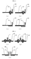
- FIG. 3 (1), (2), (3) and (4) are expanded sectional views showing embodiments of the part held by means of a supporting member at an outer peripheral edge or at a peripheral edge of the central hole both of a circular light transmitting ceramics plate in the chemical vapor deposition apparatus of the present invention.
- FIG. 4 (1), (2) and (3) are expanded sectional views showing embodiments of the part held by means of a supporting member at central portion of the circular or discus light transmitting ceramics plate in the chemical vapor deposition apparatus of the present invention.
- FIG. 5 (1) and (2) are plan views showing embodiments of light transmitting ceramics plates in the chemical vapor deposition apparatus of the present invention.
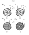
- FIGS. 6 and 7 are plan views showing embodiments of supporting members for holding or reinforcing the light transmitting member from downsides in the chemical vapor deposition apparatus of the present invention.
- the chemical vapor deposition apparatus of the present invention comprises a susceptor 2 for mounting a substrate 1 thereon, a heater 3 for heating the substrate 1, a feed gas introduction portion 4 for supplying the feed gas over the substrate 1 and a reaction gas exhaust portion 5.
- a light transmitting ceramics plate 7 held or reinforced by means of at least one of a peripheral edge supporting member 6A or a central portion supporting member 6B each shown in the expanded cross sectional views of FIGS. 3 and 4, preferably held or reinforced by means of a supporting member 6C shown in FIG. 3 (2) or (4) and FIG. 4 (1) or (2) is disposed.
- FIG. 1 the chemical vapor deposition apparatus of the present invention
- a gear drive 8 portions where gears mutually engaging both peripheral edge of the susceptor and a driving gear are disposed for revolving the susceptor 2
- a heat insulator plate 9 for revolving the susceptor 2
- plural of substrates 1 may be mounted on the susceptor 2 as shown in FIGS. 1 and 2.
- a rotary axis 11 for revolving the susceptor may be provided as shown in FIG. 2 replacing with the gear drive 8 in FIG. 1.
- the light transmitting ceramics plate 7 is disposed with a gap facing the substrate 1, the susceptor 2 or the heater 3.
- the light transmitting ceramics plate 7 is disposed so that the feed gas supplied through the feed gas introduction portion 4 or the reaction gas generated after the reaction does not reach onto the surface of the heater 3. Meanwhile, with regard to the conventional chemical vapor deposition apparatus, without light transmitting ceramics plate 7, the feed gas and reaction gas will penetrate through a gap, for example, at an outer periphery of the susceptor 2 revolving, at an outer periphery of the substrate 1 rotating, and so on resultantly reaching onto the heater 3.
- the outer peripheral edge supporting member 6A of the present invention fills a role of supporting the light transmitting ceramics plate 7 at its side
- the central portion supporting member 6B fills a role of supporting the light transmitting ceramics plate 7 at its center
- the supporting member 6C fills a role of mainly reinforcing the light transmitting ceramics plate 7 together with a role of supporting it from downside.
- the light transmitting ceramics plate 7 is usually circular or discus as shown in FIG. 5, without being limited to however, its contour or configuration of the internal circumference may be quadrangle, pentagon, hexagon, octagon, polygon, etc.
- an outer peripheral edge 12 is partially or entirely held by means of the outer peripheral edge supporting member 6A, or by means of both the outer peripheral edge supporting member 6A and the supporting member 6C as shown, for example, in FIG. 3 as usual, and a peripheral edge 13 of its central hole is partially or entirely held by means of the central portion supporting member 6B, or by means of both the central portion supporting member 6B and the supporting member 6C as shown, for example, in FIG.
- the outer peripheral edge 12 is partially or entirely held by means of the outer peripheral edge supporting member 6A, or by means of both the outer peripheral edge supporting member 6A and the supporting member 6C as shown, for example, in FIG. 3 as usual, and its central part is partially or entirely held by means of both the central portion supporting member 6B and the supporting member 6C as shown, for example, in FIG. 4 (1).
- the supporting member is not particularly limited, holding, for example, together with a volt, merely by means of the outer peripheral edge supporting member 6A or by means of the central portion supporting member 6B as shown in FIGS. 3 and 4 is practical.
- the chemical vapor deposition apparatus shown in FIGS. 1 and 2 they have structures surrounding the heater 3 by an insulator plate 9, the light transmitting ceramics plate 7 and the supporting members 6A and 6B.
- an introduction tube introducing an extra inert gas for fulfilling the inner structure with an inert gas.
- the inert gas include a nitrogen gas, a helium gas, a neon gas, an argon gas, a krypton gas, a xenon gas and a radon gas, while the nitrogen gas is frequently employed as usual.
- the structure it is desirable that a structure having an enhanced sealing property is provided for making a furiously corrosive gas used for film formation hardly invade.
- the gap between the heater 3 and the light transmitting ceramics plate 7 together with the gap between the light transmitting ceramics plate 7 and the susceptor 2 they are usually 1 to 20 mm, preferably 3 to 15 mm, further preferably 5 to 10 mm.
- the gap is in a range of from 1 mm to 20 mm, the heater can be protected from the corrosive gas.
- the gap exceeds 20 mm, a heating effect of the heater reduces.
- the ceramics plate 7 shown in FIG. 5 is circular and discus, there may be a case where a tremendous temperature distribution generates towards inner facial direction depending on an actual practical situation. In such a situation, a specific value of a coefficient of thermal expansion in the material for the ceramics plate 7 may cause a large elastic deformation, or further cause a breakdown induced by the deformation. For example, when a ceramics plate with a diameter of 600 mm is held at a temperature 1,000 °C higher than a room temperature, and when the coefficient of thermal expansion in the material is 5 ⁇ 10 -6 / °C, the ceramics plate will expand 3 mm along a direction of its diameter.
- the ceramics plate 7 is divided into parts and assembled in a manner that the thermal deformation may be buffered.
- specific examples of dividing include concentric circular, sectorial, partially or entirely dividing along its circumference after concentric circular divide, partially or entirely dividing along its radius after sectorial divide, etc.
- the light transmitting ceramics plate 7 is fixed in its peripheral portion and in its central portion by means of the supporting members 6A and 6B, a hang down caused by the plastic deformation of the light transmitting ceramics plate can be suppressed as compared with a case where only its outer peripheral edge is held by means of the supporting member.
- a quartz plate is employed as the light transmitting ceramics plate, for example, apprehensions such as a contact with other portion or a breakdown caused by the hang down of the quartz plate will disappear, and a long term stable chemical vapor deposition can be conducted.
- a supporting member (preferably a heat-resistant supporting member) 6C as shown in FIGS. 6 and 7 may be provided under the light transmitting ceramics plate 7 in a manner as shown in FIG. 3 (2) and (4) or FIG. 4 for holding or for reinforcing, resultantly enabling to powerfully suppress the hang down of the light transmitting ceramics plate 7.
- examples include structures as shown in FIG. 7 (1) and (2), consisting of an outer peripheral part 14, a central part 15 and a coupling part 16 for coupling them or a geometrical coupling part 17, and as shown in FIG. 7 (3) and (4), structures consisting of the outer peripheral part 14 and the geometrical coupling member 17 disposed inside the outer peripheral part 14.
- the outer peripheral part 14 and the central part 15 mainly fill a role of holding the light transmitting ceramics plate 7 from downside together with a role of reinforcing the ceramics plate 7, and the coupling part 16 or the geometrical coupling part 17 mainly fills a role of suppressing the hang down of the light transmitting ceramics plate 7 caused by its plastic deformation.
- typical examples include mesh, radial, spiral, vertical stripe, horizontal stripe and those combination.
- the supporting member 6C it is usually round fitting with the light transmitting ceramics plate; however, it may be quadrangle, pentagon, hexagon, octagon, polygon and so on without being limited to them.
- An outer diameter of the supporting member 6C is usually the same as or approximately the same as the outer diameter of the light transmitting ceramics plate 7.
- the supporting member 6C consists of, for example, the outer peripheral part 14, the central part 15 and the coupling part 16 for coupling them or the geometrical coupling part 17. Additionally, it is desirable that the supporting member 6C is also divided into parts and assembled in a manner that the thermal deformation may be buffered similarly as the light transmitting ceramics plate 7. Specific examples of dividing include the same as described about the light transmitting ceramics plate 7 in the foregoing.
- silicon oxide including quartz
- alumina magnesia
- yttrium oxide and further, oxide-based ceramics such as MgAl 2 O 4 or aluminumoxynitride, and nitride-based ceramics such as aluminumnitride or so is employed as a material for composing the light transmitting ceramics plate.
- oxide-based ceramics such as MgAl 2 O 4 or aluminumoxynitride
- nitride-based ceramics such as aluminumnitride or so is employed as a material for composing the light transmitting ceramics plate.
- any material having heat resistance against the temperature of around 1,200 °C , transmitting heat rays radiated from the heater, and having corrosion resistance against the feed gas and the reaction gas is also employable.
- the thickness of the light transmitting ceramics plate is usually within a range of from about 0.5 to 10 mm, its outer diameter is usually within a range of about 100 to 1,000 mm, and when it has a central hole, the diameter of the central hole is usually within a range of from about 2 to 200 mm.
- metals such as carbon steel, manganese steel, chrome steel, molybdenum steel, stainless steel, nickel steel, tungsten steel and further, alloys, metallic oxides, ceramics, carbon, and so on are employed as a material for composing the supporting member.
- a heat-resistant material having more superior mechanical strength at a temperature within a range of from 800 to 1,300 °C than the light transmitting ceramics plate 7 is particularly employed for the supporting member 6C.
- the heat-resistant material for the supporting member include metals such as molybdenum, tungsten or so; heat-resistant alloys such as Inconel or so; metal oxides such as alumina, aluminumoxynitride, magnesia, zirconia or so; nitride-based ceramics such as boron nitride, silicon nitride, zirconium nitride, titanium nitride, tungsten nitride or so; carbide-based ceramics such as boron carbide, silicon carbide, zirconium carbide, titanium carbide, tungsten carbide, tantalum carbide or so; boride-based ceramics such as nitrogen boride, carbon boride, titanium boride or so; and carbon.
- the carbon because there is a case where normal isotropic graphite has not so great corrosion resistance, it is preferable to employ a carbon (pyrolytic carbon) prepared by chemical vapor deposition, a graphite covered with pyrolytic carbon, glassy carbon, a graphite covered with glassy carbon, a graphite covered with tantalum carbide, a graphite covered with silicon carbide, etc. Further, two kinds or more among those in combination may be employable. Moreover, when the supporting member 6C is not light transmitting, it obstruct heat rays radiated from the heater to effectively reach onto the susceptor and accordingly, it is necessary to reduce cross sectional area of the supporting member 6C observed from the heater as small as possible.
- preferable examples of configuration of reinforcing parts include wire having diameter within a range from 0.5 to 5 mm, or a mesh using the wire. Further, a favorite value about the cross sectional area of the reinforcing parts is, for example, 50 % or smaller, preferably 40 % or smaller and more preferably 20 % or smaller.
- quartz has very small coefficient of thermal expansion among the light transmitting ceramics, even a large member made of quartz exhibits small thermal elastic deformation and is favorably employed in the present invention.
- the materials for the supporting member 6C they are thoroughly classified into favorably light transmitting materials and slightly light transmitting materials.
- the former include sapphire, alumina, aluminumoxynitride and so on; and examples of the latter include heat-resistant metals, etc.
- the heat-resistant metals are tough against thermal bombardment and mechanical shock resultantly employable as the supporting member in the present invention.
- providing the favorable light transmitting reinforcing member between the supporting member and the light transmitting ceramics plate enables to enhance the reinforcing effect without losing transmission of the heat rays resultantly making it applicable for the present invention.
- after such structures are adopted, even when the coefficient of thermal expansion of the light transmitting reinforcing member is not so small, they are preferable because numbers of divided reinforcing member are assembled and further supported by another reinforcing member having slight light transmitting property.
- quartz may evaporate at an elevated temperature.
- quartz as the light transmitting ceramics and heating it up to about 1,100 °C or more in an atmosphere of hydrogen will cause a case sputtering quartz powder over the surface of the susceptor.
- the color of the surface on the heater side of the susceptor changes and its absorption factor about heat rays from the heater varies.
- a necessary power for heating the susceptor also varies with passage of time, and accordingly, stable film formation over long term becomes impossible.
- any light transmitting ceramics material except quartz is employed together with quartz, it has an effect of suppressing vaporization of quartz resultantly enables to stably form a film for a long term. Therefore, the material except quartz is favorably employed as a specific example in the present invention.
- the material for the heater employable in the present invention include metals having high melting point such as molybdenum, tungsten and so on; graphite, heat-resistant and electrically conductive ceramics such as silicon carbide, etc. Because the silicon carbide has subliming ability in a reductive atmosphere at an elevated temperature, when it is heated, it is desirably held in an inert gas ambient atmosphere such as nitrogen, argon, etc. In accordance with the present invention, even a material with low corrosion-resistant property against ammonia at an elevated temperature such as graphite can be employed for the heater. However, covering the heater with an ammonia-resistant material will improve its reliability for an unexpected situation. Specific examples of the ammonia-resistant material suitable for covering graphite employed as the heater include pyrolytic carbon, glassy carbon, tantalum carbide, silicon carbide, etc.
- a discus susceptor (diameter: 560 mm, thickness: 11 mm), a heater, a feed gas introduction portion, a gas guiding member and a reaction gas exhaust portion inside of a reactor chamber made of stainless steel, and further providing a circular light transmitting ceramics plate (quartz plate) held at its peripheral edge by an outer peripheral edge supporting member 6A (boron nitride) and at its peripheral edge of a central hole by a central portion supporting member 6B (boron nitride), a chemical vapor deposition apparatus as shown in FIG. 1 was assembled. Additionally, regarding with the light transmitting ceramics plate, its diameter was 650 mm, its thickness was 3 mm, and a diameter of its central hole was 32 mm.
- the light transmitting ceramics plate was supported from downside and reinforced by means of a supporting member 6C as shown in FIG. 6 (3) and composed of a peripheral part (outer diameter: 650 mm, width: 30 mm, thickness: 3 mm) made of carbon, a central part (outer diameter: 62 mm, width: 30 mm, thickness: 3 mm) made of carbon and a coupling part with a mesh structure (spacing: 10 mm) made of molybdenum. Furthermore, the gap between the light transmitting plate and the heater was 7 mm, the gap between the light transmitting plate and the susceptor being also 7 mm.
- the following heat test was carried out. Namely, after replacing the atmospheric air in the reactor chamber with nitrogen gas and heating the susceptor so that a thermocouple provided adjacent to the heater up to a temperature of 1200 °C, the temperature was maintained for totally 18 hours.
- Chemical vapor deposition apparatuses were assembled in the same manner as Example 1 except that composing materials for the supporting members 6A and 6B each holding both the outer peripheral edges and the inner peripheral edges of the central holes in the light transmitting ceramics plates were replaced with a pair of stainless and alumina, a pair of stainless and Inconel and a pair of stainless and carbon respectively.
- Example 2 the heat tests were conducted in the same manner as Example 1 except that those chemical vapor deposition apparatuses were employed respectively.
- the hangs down of the light transmitting ceramics plate were hardly observed in any of all, and even the maximum value was 1 mm or shorter.
- Chemical vapor deposition apparatuses were assembled in the same manners as Example 1, except that the supporting member 6C for supporting the light transmitting ceramics plate from downside was replaced with those as shown in FIG. 6 (2) (diameter of molybdenum wire: 3 mm), FIG. 6 (4) (spacing of mesh: 10 mm), FIG. 7 (1) (diameter of molybdenum wire: 3 mm), and FIG. 7 (2) (diameter of molybdenum wire: 3 mm) respectively.
- Example 2 the heat tests were conducted in the same manner as Example 1 except that those chemical vapor deposition apparatuses were employed respectively.
- the hangs down of the light transmitting ceramics plate were hardly observed in any of all, and even the maximum value was 1 mm or shorter.
- Chemical vapor deposition apparatuses were assembled in the same manners as Example 1 except that composing materials for the coupling part 16 in the supporting member 6C for supporting the light transmitting ceramics plates from downside were replaced with tungsten, Inconel and boron nitride respectively.
- Example 2 the heat tests were conducted in the same manner as Example 1 except that those chemical vapor deposition apparatuses were employed respectively.
- the hangs down of the light transmitting ceramics plate were hardly observed in any of all, and even the maximum value was 1 mm or shorter.
- Chemical vapor deposition apparatuses were assembled in the same manners as Example 1 except that composing material for the light transmitting ceramics plate was replaced with sapphire, alumina, aluminumoxynitride respectively.
- Example 2 the heat tests were conducted in the same manner as Example 1 except that those chemical vapor deposition apparatuses were employed respectively.
- the hangs down of the light transmitting ceramics plate were hardly observed in any of all, and even the maximum value was 1 mm or shorter.
- a circular susceptor (diameter: 560 mm, thickness: 11 mm), a heater, a feed gas introduction portion, a gas guiding member and a reaction gas exhaust portion inside of a reactor chamber made of stainless steel, and further providing a circular light transmitting ceramics plate held at its outer peripheral edge by a peripheral edge supporting member 6A and at its inner peripheral edge of a central hole by a central portion supporting member 6B, a chemical vapor deposition apparatus as shown in FIG. 2 was assembled.
- the light transmitting ceramics plate was prepared by laminating quartz and sapphire each other (thickness: 1.5 mm each respectively), and it was set in the apparatus placing sapphire at bottom side.
- the chemical vapor deposition apparatus was completed exactly in the same as Example 1 except the above description. Then, the heat test was conducted in the same manner as Example 1 except that the above chemical vapor deposition apparatus was employed. As a result, the hang down of the light transmitting ceramics plate was hardly observed, and even the maximum value was 1 mm or shorter.
- a circular susceptor (diameter: 280 mm, thickness: 11 mm), a heater, a feed gas introduction portion, a gas guiding member and a reaction gas exhaust portion inside of a reactor chamber made of stainless steel, and further providing a discus light transmitting ceramics plate (quartz plate) without hole at its center and held at its peripheral edge and at its central portion by means of supporting members 6A and 6B (boron nitride), a chemical vapor deposition apparatus as shown in FIG. 1 was assembled.
- the light transmitting ceramics plate its diameter was 300 mm, its thickness was 5 mm. However, the heat-resistant support member 6C was not used. In addition, a gap between the light transmitting ceramics plate and the heater was 7 mm, and a gap between the light transmitting ceramics plate and the susceptor was also 7 mm.
- Example 2 the heat test was conducted in the same manner as Example 1 except that the above chemical vapor deposition apparatus was employed. As a result, the hang down of the light transmitting ceramics plate was short and even the maximum value was about 1 to 2 mm.
- Chemical vapor deposition apparatuses were assembled in the same manners as Example 16 except that composing material for the light transmitting ceramics plate was replaced with sapphire, alumina, aluminumoxynitride respectively.
- Example 2 the heat tests were conducted in the same manner as Example 1 except that those chemical vapor deposition apparatuses were employed respectively.
- the hangs down of the light transmitting ceramics plates were short in any of all, and even the maximum values were about 1 to 2 mm respectively.
- a chemical vapor deposition apparatus was assembled in the same manner as Example 1 except that the light transmitting ceramics plate was absent.
- the following corrosion resistance test was carried out. Namely, after heating the susceptor so that the thermocouple adjacent the heater up to a temperature of 1200 °C, a mixed gas of ammonia gas (20 % by volume) and hydrogen gas (80 % by volume) was flown into the reactor chamber for 20 hours.
- Tables 1 and 2 shows conditions and results of the heat tests in Examples 1 to 19.
- Table 3 shows conditions and results of corrosion resistance test in Example 1 and Comparative Example 1.
- the chemical vapor deposition apparatus whose light transmitting ceramics plate is held by means of the supporting members 6A and 6B in the present invention protects the heater from a corrosive gas without causing great hang down induced by its plastic deformation in the light transmitting ceramics plate even under an elevated temperature. Further, it is also verified that the chemical vapor deposition apparatus of the present invention employing the heat-resistant supporting member 6C together with the supporting members 6A and 6B is capable of regulating the hang down induced by its plastic deformation.
- the chemical vapor deposition apparatus of the present invention does not employ a structure directly covering the heater with a heat-resistant material or a corrosion-resistant material, there is not any problem in a difference of coefficient of thermal expansion between a composing material of the heat source and the heat-resistant material or the corrosion-resistant material. Further, it has a structure disposing the light transmitting ceramics plate made of quartz or so whose softening point is relatively low between the heater and the substrates, and the ceramics plate is held or reinforced by means of the supporting member. Accordingly, plastic deformation of the ceramics plate at an elevated temperature is almost negligible and as a result, it is possible to reduce a renewal frequency of the ceramics plate tremendously.
- the chemical vapor deposition apparatus of the present invention enables to chemically vapor deposit stably for a long time with good reproduction property suppressing a breakdown of the heater or so even in a case of chemical vapor deposition reaction employing a furiously corrosive gas with an elevated temperature for producing a gallium nitride compound semiconductor or so.
Landscapes
- Chemical & Material Sciences (AREA)
- General Chemical & Material Sciences (AREA)
- Chemical Kinetics & Catalysis (AREA)
- Engineering & Computer Science (AREA)
- Materials Engineering (AREA)
- Mechanical Engineering (AREA)
- Metallurgy (AREA)
- Organic Chemistry (AREA)
- Health & Medical Sciences (AREA)
- Toxicology (AREA)
- Chemical Vapour Deposition (AREA)
- Crystals, And After-Treatments Of Crystals (AREA)
Applications Claiming Priority (1)
| Application Number | Priority Date | Filing Date | Title |
|---|---|---|---|
| JP2005256001 | 2005-09-05 |
Publications (3)
| Publication Number | Publication Date |
|---|---|
| EP1760170A2 true EP1760170A2 (fr) | 2007-03-07 |
| EP1760170A3 EP1760170A3 (fr) | 2007-12-05 |
| EP1760170B1 EP1760170B1 (fr) | 2011-04-06 |
Family
ID=37453019
Family Applications (1)
| Application Number | Title | Priority Date | Filing Date |
|---|---|---|---|
| EP06018282A Not-in-force EP1760170B1 (fr) | 2005-09-05 | 2006-09-01 | Appareil de dépôt chimique en phase vapeur |
Country Status (6)
| Country | Link |
|---|---|
| US (2) | US20070051316A1 (fr) |
| EP (1) | EP1760170B1 (fr) |
| KR (1) | KR20070026265A (fr) |
| CN (1) | CN1928152B (fr) |
| DE (1) | DE602006021108D1 (fr) |
| TW (1) | TWI331361B (fr) |
Cited By (2)
| Publication number | Priority date | Publication date | Assignee | Title |
|---|---|---|---|---|
| CN110885973A (zh) * | 2018-09-11 | 2020-03-17 | 上海引万光电科技有限公司 | 化学气相沉积设备 |
| CN113088935A (zh) * | 2021-03-30 | 2021-07-09 | 上海华力微电子有限公司 | 一种固定底座、lpcvd炉管及lpcvd设备 |
Families Citing this family (10)
| Publication number | Priority date | Publication date | Assignee | Title |
|---|---|---|---|---|
| EP1760170B1 (fr) * | 2005-09-05 | 2011-04-06 | Japan Pionics Co., Ltd. | Appareil de dépôt chimique en phase vapeur |
| JP5138212B2 (ja) * | 2006-12-25 | 2013-02-06 | 東京エレクトロン株式会社 | 成膜装置 |
| CN101924023A (zh) * | 2009-06-09 | 2010-12-22 | 日本派欧尼株式会社 | Iii族氮化物半导体的气相生长装置 |
| KR101155766B1 (ko) * | 2009-12-18 | 2012-06-12 | 파이니스트 주식회사 | 사파이어 히터 |
| JP5409413B2 (ja) * | 2010-01-26 | 2014-02-05 | 日本パイオニクス株式会社 | Iii族窒化物半導体の気相成長装置 |
| US8910644B2 (en) * | 2010-06-18 | 2014-12-16 | Applied Materials, Inc. | Method and apparatus for inducing turbulent flow of a processing chamber cleaning gas |
| JP2013074078A (ja) * | 2011-09-28 | 2013-04-22 | Japan Pionics Co Ltd | 気相成長装置の構成部品の洗浄装置及び洗浄方法 |
| CN108950502B (zh) * | 2018-07-23 | 2022-12-13 | 张家港康得新光电材料有限公司 | 一种面板成膜设备 |
| CN111118475A (zh) * | 2020-01-15 | 2020-05-08 | 中国科学院半导体研究所 | 用于碳化硅材料生长和后处理的高温装置及方法 |
| CN113913927A (zh) * | 2021-08-25 | 2022-01-11 | 华灿光电(苏州)有限公司 | 金属有机化学气相沉积设备及其使用方法 |
Citations (7)
| Publication number | Priority date | Publication date | Assignee | Title |
|---|---|---|---|---|
| JPH05206100A (ja) | 1992-01-24 | 1993-08-13 | Fujitsu Ltd | 半導体製造装置 |
| JPH0817745A (ja) | 1994-06-30 | 1996-01-19 | Toshiba Mach Co Ltd | ヒータ |
| JPH11233244A (ja) | 1998-02-12 | 1999-08-27 | Sumiju Sn Business:Kk | Cvd装置用熱板 |
| US6254687B1 (en) | 1999-03-26 | 2001-07-03 | Japan Process Engineering, Ltd. | Chemical vapor deposition system with reduced material deposition on chamber wall surfaces |
| EP1148151A2 (fr) | 2000-04-18 | 2001-10-24 | Nhk Spring Co.Ltd. | Elément de chauffage en céramique et dispositif de formation des couches utilisant celui ci |
| EP1154039A1 (fr) | 1993-01-21 | 2001-11-14 | Moore Epitaxial, Inc. | Appareil de traitement thermique rapide pour le traitement de tranches de semiconducteurs |
| US20030186517A1 (en) | 2002-04-01 | 2003-10-02 | Mikio Takagi | Method of and apparatus for manufacturing semiconductor device |
Family Cites Families (14)
| Publication number | Priority date | Publication date | Assignee | Title |
|---|---|---|---|---|
| JPH0737670B2 (ja) | 1991-04-26 | 1995-04-26 | 株式会社日本生産技術研究所 | ライン式プラズマcvd装置 |
| JP3553204B2 (ja) * | 1995-04-28 | 2004-08-11 | アネルバ株式会社 | Cvd装置 |
| US6143477A (en) * | 1998-09-08 | 2000-11-07 | Amtech Systems, Inc. | Dual wavelength UV lamp reactor and method for cleaning/ashing semiconductor wafers |
| CN1077607C (zh) * | 1998-11-03 | 2002-01-09 | 南京大学 | 光辐射加热金属有机化学汽相淀积氮化镓生长方法与装置 |
| JP3545962B2 (ja) | 1999-03-23 | 2004-07-21 | 三菱電線工業株式会社 | GaN系化合物半導体結晶の成長方法及び半導体結晶基材 |
| JP2001250783A (ja) * | 2000-03-08 | 2001-09-14 | Japan Pionics Co Ltd | 気相成長装置及び気相成長方法 |
| JP4540796B2 (ja) * | 2000-04-21 | 2010-09-08 | 東京エレクトロン株式会社 | 石英ウインドウ、リフレクタ及び熱処理装置 |
| US6559424B2 (en) * | 2001-01-02 | 2003-05-06 | Mattson Technology, Inc. | Windows used in thermal processing chambers |
| JP2003213421A (ja) * | 2002-01-21 | 2003-07-30 | Hitachi Kokusai Electric Inc | 基板処理装置 |
| JP3983631B2 (ja) * | 2002-04-09 | 2007-09-26 | シャープ株式会社 | 衛星放送受信装置 |
| JP2003133225A (ja) | 2002-07-15 | 2003-05-09 | Ibiden Co Ltd | 半導体製品加熱用ヒータ |
| KR100450643B1 (ko) * | 2003-09-26 | 2004-10-01 | 코닉시스템 주식회사 | 플라즈마 급속열처리 장치 |
| US7396415B2 (en) * | 2005-06-02 | 2008-07-08 | Asm America, Inc. | Apparatus and methods for isolating chemical vapor reactions at a substrate surface |
| EP1760170B1 (fr) * | 2005-09-05 | 2011-04-06 | Japan Pionics Co., Ltd. | Appareil de dépôt chimique en phase vapeur |
-
2006
- 2006-09-01 EP EP06018282A patent/EP1760170B1/fr not_active Not-in-force
- 2006-09-01 DE DE602006021108T patent/DE602006021108D1/de active Active
- 2006-09-04 TW TW095132519A patent/TWI331361B/zh not_active IP Right Cessation
- 2006-09-04 KR KR1020060084766A patent/KR20070026265A/ko not_active Ceased
- 2006-09-04 CN CN2006101286726A patent/CN1928152B/zh not_active Expired - Fee Related
- 2006-09-05 US US11/514,927 patent/US20070051316A1/en not_active Abandoned
-
2009
- 2009-07-02 US US12/497,428 patent/US8277893B2/en not_active Expired - Fee Related
Patent Citations (7)
| Publication number | Priority date | Publication date | Assignee | Title |
|---|---|---|---|---|
| JPH05206100A (ja) | 1992-01-24 | 1993-08-13 | Fujitsu Ltd | 半導体製造装置 |
| EP1154039A1 (fr) | 1993-01-21 | 2001-11-14 | Moore Epitaxial, Inc. | Appareil de traitement thermique rapide pour le traitement de tranches de semiconducteurs |
| JPH0817745A (ja) | 1994-06-30 | 1996-01-19 | Toshiba Mach Co Ltd | ヒータ |
| JPH11233244A (ja) | 1998-02-12 | 1999-08-27 | Sumiju Sn Business:Kk | Cvd装置用熱板 |
| US6254687B1 (en) | 1999-03-26 | 2001-07-03 | Japan Process Engineering, Ltd. | Chemical vapor deposition system with reduced material deposition on chamber wall surfaces |
| EP1148151A2 (fr) | 2000-04-18 | 2001-10-24 | Nhk Spring Co.Ltd. | Elément de chauffage en céramique et dispositif de formation des couches utilisant celui ci |
| US20030186517A1 (en) | 2002-04-01 | 2003-10-02 | Mikio Takagi | Method of and apparatus for manufacturing semiconductor device |
Cited By (2)
| Publication number | Priority date | Publication date | Assignee | Title |
|---|---|---|---|---|
| CN110885973A (zh) * | 2018-09-11 | 2020-03-17 | 上海引万光电科技有限公司 | 化学气相沉积设备 |
| CN113088935A (zh) * | 2021-03-30 | 2021-07-09 | 上海华力微电子有限公司 | 一种固定底座、lpcvd炉管及lpcvd设备 |
Also Published As
| Publication number | Publication date |
|---|---|
| US20070051316A1 (en) | 2007-03-08 |
| CN1928152A (zh) | 2007-03-14 |
| TWI331361B (en) | 2010-10-01 |
| US20090269938A1 (en) | 2009-10-29 |
| US8277893B2 (en) | 2012-10-02 |
| DE602006021108D1 (de) | 2011-05-19 |
| EP1760170A3 (fr) | 2007-12-05 |
| KR20070026265A (ko) | 2007-03-08 |
| TW200715378A (en) | 2007-04-16 |
| EP1760170B1 (fr) | 2011-04-06 |
| CN1928152B (zh) | 2010-12-22 |
Similar Documents
| Publication | Publication Date | Title |
|---|---|---|
| US8277893B2 (en) | Chemical vapor deposition apparatus | |
| US5680013A (en) | Ceramic protection for heated metal surfaces of plasma processing chamber exposed to chemically aggressive gaseous environment therein and method of protecting such heated metal surfaces | |
| JP4430769B2 (ja) | セラミックス加熱治具 | |
| KR102367939B1 (ko) | 내플라즈마성 코팅을 갖는 섀도우 마스크 | |
| EP1796149A1 (fr) | Dispositif de serrage en quartz et équipement de fabrication de semi-conducteurs | |
| US20070215596A1 (en) | Semiconductor Batch Heating Assembly | |
| WO2006006391A1 (fr) | Équipement de chauffage de plaque et équipement de fabrication de semi-conducteur | |
| US9351344B2 (en) | Ceramic heater | |
| JP2013123028A (ja) | 熱処理装置 | |
| JP2010177595A (ja) | 半導体製造装置用ウエハ保持体、及びそれを備えた半導体製造装置 | |
| JPH1174064A (ja) | ウエハ加熱装置 | |
| US20070095291A9 (en) | Holder for Use in Semiconductor or Liquid-Crystal Manufacturing Device and Semiconductor or Liquid-Crystal Manufacturing Device in Which the Holder Is Installed | |
| JP2021080567A (ja) | 耐プラズマコーティングを有するシャドウマスク | |
| US20040108314A1 (en) | Heating apparatus which has electrostatic adsorption function, and method for producing it | |
| JP4874743B2 (ja) | 窒化ガリウム系化合物半導体の気相成長装置 | |
| US20010052324A1 (en) | Device for producing and processing semiconductor substrates | |
| KR20150001781U (ko) | 히터 조립체 | |
| KR100361067B1 (ko) | 염소계 가스에 대한 내식성 부재 | |
| JP2011100844A (ja) | 静電吸着機能を有する装置及びその製造方法 | |
| KR100976547B1 (ko) | 유도가열 서셉터 및 그 제조방법 | |
| JP2007096280A5 (ja) | 窒化ガリウム系化合物半導体の気相成長装置 | |
| KR20020067640A (ko) | 다이아몬드 코팅 부재 | |
| US20250079233A1 (en) | Ceramic susceptor | |
| KR101930788B1 (ko) | 기판 프로세싱 챔버의 냉각기 | |
| KR20150030349A (ko) | 웨이퍼 캐리어 및 그 제조방법 |
Legal Events
| Date | Code | Title | Description |
|---|---|---|---|
| PUAI | Public reference made under article 153(3) epc to a published international application that has entered the european phase |
Free format text: ORIGINAL CODE: 0009012 |
|
| AK | Designated contracting states |
Kind code of ref document: A2 Designated state(s): AT BE BG CH CY CZ DE DK EE ES FI FR GB GR HU IE IS IT LI LT LU LV MC NL PL PT RO SE SI SK TR |
|
| AX | Request for extension of the european patent |
Extension state: AL BA HR MK YU |
|
| PUAL | Search report despatched |
Free format text: ORIGINAL CODE: 0009013 |
|
| AK | Designated contracting states |
Kind code of ref document: A3 Designated state(s): AT BE BG CH CY CZ DE DK EE ES FI FR GB GR HU IE IS IT LI LT LU LV MC NL PL PT RO SE SI SK TR |
|
| AX | Request for extension of the european patent |
Extension state: AL BA HR MK YU |
|
| 17P | Request for examination filed |
Effective date: 20080331 |
|
| 17Q | First examination report despatched |
Effective date: 20080506 |
|
| AKX | Designation fees paid |
Designated state(s): DE FR GB |
|
| GRAP | Despatch of communication of intention to grant a patent |
Free format text: ORIGINAL CODE: EPIDOSNIGR1 |
|
| GRAS | Grant fee paid |
Free format text: ORIGINAL CODE: EPIDOSNIGR3 |
|
| GRAA | (expected) grant |
Free format text: ORIGINAL CODE: 0009210 |
|
| RIN1 | Information on inventor provided before grant (corrected) |
Inventor name: TAKAMATSU, YUKICHIC/O JAPAN PIONICS CO., LTD. Inventor name: SUDA, NOBORU Inventor name: KOMIYA, YOSHINAOC/O JAPAN PIONICS CO., LTD. Inventor name: YONEYAMA, TAKEOC/O JAPAN PIONICS CO., LTD. Inventor name: ISHIHAMA, YOSHIYASUC/O JAPAN PIONICS CO., LTD. Inventor name: OHORI, TATSUYAC/O ASEC, INC. Inventor name: IYECHIKA, YASUSHIC/O ASEC, INC. Inventor name: SHIINA, KAZUSHIGEC/O ASEC, INC. |
|
| AK | Designated contracting states |
Kind code of ref document: B1 Designated state(s): DE FR GB |
|
| REG | Reference to a national code |
Ref country code: GB Ref legal event code: FG4D |
|
| REF | Corresponds to: |
Ref document number: 602006021108 Country of ref document: DE Date of ref document: 20110519 Kind code of ref document: P |
|
| REG | Reference to a national code |
Ref country code: DE Ref legal event code: R096 Ref document number: 602006021108 Country of ref document: DE Effective date: 20110519 |
|
| PLBE | No opposition filed within time limit |
Free format text: ORIGINAL CODE: 0009261 |
|
| STAA | Information on the status of an ep patent application or granted ep patent |
Free format text: STATUS: NO OPPOSITION FILED WITHIN TIME LIMIT |
|
| 26N | No opposition filed |
Effective date: 20120110 |
|
| REG | Reference to a national code |
Ref country code: DE Ref legal event code: R097 Ref document number: 602006021108 Country of ref document: DE Effective date: 20120110 |
|
| PGFP | Annual fee paid to national office [announced via postgrant information from national office to epo] |
Ref country code: GB Payment date: 20120920 Year of fee payment: 7 |
|
| PGFP | Annual fee paid to national office [announced via postgrant information from national office to epo] |
Ref country code: DE Payment date: 20120829 Year of fee payment: 7 |
|
| PGFP | Annual fee paid to national office [announced via postgrant information from national office to epo] |
Ref country code: FR Payment date: 20121008 Year of fee payment: 7 |
|
| GBPC | Gb: european patent ceased through non-payment of renewal fee |
Effective date: 20130901 |
|
| REG | Reference to a national code |
Ref country code: FR Ref legal event code: ST Effective date: 20140530 |
|
| REG | Reference to a national code |
Ref country code: DE Ref legal event code: R119 Ref document number: 602006021108 Country of ref document: DE Effective date: 20140401 |
|
| PG25 | Lapsed in a contracting state [announced via postgrant information from national office to epo] |
Ref country code: GB Free format text: LAPSE BECAUSE OF NON-PAYMENT OF DUE FEES Effective date: 20130901 |
|
| PG25 | Lapsed in a contracting state [announced via postgrant information from national office to epo] |
Ref country code: DE Free format text: LAPSE BECAUSE OF NON-PAYMENT OF DUE FEES Effective date: 20140401 Ref country code: FR Free format text: LAPSE BECAUSE OF NON-PAYMENT OF DUE FEES Effective date: 20130930 |