EP1775773A2 - Flexible Bildanzeigevorrichtung - Google Patents
Flexible Bildanzeigevorrichtung Download PDFInfo
- Publication number
- EP1775773A2 EP1775773A2 EP06255303A EP06255303A EP1775773A2 EP 1775773 A2 EP1775773 A2 EP 1775773A2 EP 06255303 A EP06255303 A EP 06255303A EP 06255303 A EP06255303 A EP 06255303A EP 1775773 A2 EP1775773 A2 EP 1775773A2
- Authority
- EP
- European Patent Office
- Prior art keywords
- flat panel
- panel display
- flexible flat
- flexible
- display according
- Prior art date
- Legal status (The legal status is an assumption and is not a legal conclusion. Google has not performed a legal analysis and makes no representation as to the accuracy of the status listed.)
- Granted
Links
Images




Classifications
-
- H—ELECTRICITY
- H10—SEMICONDUCTOR DEVICES; ELECTRIC SOLID-STATE DEVICES NOT OTHERWISE PROVIDED FOR
- H10K—ORGANIC ELECTRIC SOLID-STATE DEVICES
- H10K59/00—Integrated devices, or assemblies of multiple devices, comprising at least one organic light-emitting element covered by group H10K50/00
- H10K59/10—OLED displays
- H10K59/12—Active-matrix OLED [AMOLED] displays
- H10K59/131—Interconnections, e.g. wiring lines or terminals
-
- H—ELECTRICITY
- H05—ELECTRIC TECHNIQUES NOT OTHERWISE PROVIDED FOR
- H05B—ELECTRIC HEATING; ELECTRIC LIGHT SOURCES NOT OTHERWISE PROVIDED FOR; CIRCUIT ARRANGEMENTS FOR ELECTRIC LIGHT SOURCES, IN GENERAL
- H05B33/00—Electroluminescent light sources
- H05B33/12—Light sources with substantially two-dimensional [2D] radiating surfaces
- H05B33/22—Light sources with substantially two-dimensional [2D] radiating surfaces characterised by the chemical or physical composition or the arrangement of auxiliary dielectric or reflective layers
-
- H—ELECTRICITY
- H10—SEMICONDUCTOR DEVICES; ELECTRIC SOLID-STATE DEVICES NOT OTHERWISE PROVIDED FOR
- H10K—ORGANIC ELECTRIC SOLID-STATE DEVICES
- H10K2102/00—Constructional details relating to the organic devices covered by this subclass
- H10K2102/301—Details of OLEDs
- H10K2102/311—Flexible OLED
Definitions
- the present invention relates to a flexible flat panel display, and more particularly, to a flexible flat panel display which prevents electronic units such as a driving Integrated Circuit (IC) and a flexible printed circuit board from being separated from the flexible flat panel display even when the flexible flat panel display is bent.
- IC Integrated Circuit
- a flat panel display such as a liquid crystal display, an organic light emitting device, or an inorganic light emitting device has a flat shape and can be used as a flexible display.
- the flat panel display is bonded to a flexible printed circuit board.
- a driving Integrated Circuit (IC) is directly mounted on the flexible display.
- the flexible printed circuit board or the driving IC is bonded to a pad unit formed on an edge of the flat panel display via an anisotropy conductive adhesive.
- the flexible printed circuit board or the driving IC is attached to a lateral or longitudinal side of a flat panel display.
- the flexible flat panel display can be bent in at least one direction, and can be used in a bent state.
- the flexible flat panel display can be bent in a specific direction and attached to a cylinder or the like.
- the flexible flat panel display when the flexible flat panel display is bent, the flexible printed circuit board or the driving IC placed on a bent side will likely separate from the flexible flat panel display due to the bending stress. In this case, the flat panel display is electrically open and an image cannot be displayed.
- the present invention seeks to provide a flexible flat panel display in which a flexible printed circuit board and a driving Integrated Circuit (IC) are not separated from the flexible flat panel display even when the flexible flat panel display is bent.
- IC Integrated Circuit
- a flexible flat panel display comprises the features of Claim 1. Preferred features of this aspect of the invention are set out in Claims 2 to 19.
- a flexible flat panel display including: a display area adapted to be bent in at least one direction and to display an image; a plurality of first wires intersecting the display area and extending along sides of the display area, the sides of the display area being bent; and a plurality of second wires intersecting the display area and extending along other sides of the display area, the other sides of the display area not being bent; the first wires and the second wires extending along the sides of the display area to locations external to the display area.
- the first wires and the second wires preferably extend in opposite directions external to the display area.
- the first wires and the second wires alternatively preferably extend in the same direction external to the display area.
- some of the first wires and second wires alternatively preferably extend in one bending direction of the bent sides of the display area, and the other of the first wires and second wires preferably extend in another bending direction different from the one bending direction.
- FIG. 1 is a plan view of a flexible flat panel display according to an embodiment of the present invention
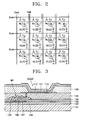
- FIG. 2 is a circuit diagram of pixels of an Active-Matrix (AM) organic light emitting display, which is an example of a display area of FIG. 1;
- AM Active-Matrix
- FIG. 3 is a cross-sectional view of an example of a portion of the AM organic light emitting display of FIG. 2;
- FIG. 4 is a plan view of a flexible flat panel display according to another embodiment of the present invention.
- FIG. 5 is a plan view of a flexible flat panel display according to another embodiment of the present invention.
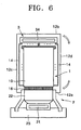
- FIG. 6 is a plan view of a flexible flat panel display according to another embodiment of the present invention.
- FIG. 7 is a plan view of a flexible flat panel display according to another embodiment of the present invention.
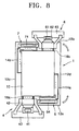
- FIG. 8 is a plan view of a flexible flat panel display according to another embodiment of the present invention.
- region' is used to denote a field adjacent a side of some other component. This is intended to denote general proximity.
- the regions do not have predetermined boundaries and can vary in size and overlap.
- FIG. 1 is a plan view of a flexible flat panel display according to an embodiment of the present invention.
- the flexible flat panel display includes a flexible display unit 1, and a first electronic unit 2 and a second electronic unit 3 bonded to the display unit 1.
- the flexible display unit 1, as shown in FIG. 1, can have a rectangular shape, and includes a first side 12a and a second side 12b, which are short sides parallel to each other, and a third side 12c and a fourth side 12d which are long sides parallel to each other.
- the flexible display unit 1 can be bent in at least one direction.
- the flexible display unit 1 can be bent in the arrow directions indicated in FIG. 1. That is, the first side 12a through the fourth side 12d of the flexible display unit 1 can be bent, and the flexible display unit 1 can be used in a state in which the long sides, i.e., the third and fourth sides 12c and 12d, are bent.
- a display area 10 is formed in the center of the flexible display unit 1.
- the display area 10 can be formed using an Active-Matrix (AM) organic light emitting device, as shown in FIG. 2.
- AM Active-Matrix
- each pixel of the AM organic light emitting device includes at least two Thin Film Transistors (TFTs), that is, a driving TFT M 1 and a switching TFT M 2 , a storage capacitor C st and an Organic Light Emitting Diode (OLED).
- TFTs Thin Film Transistors
- the switching TFT M 2 is turned on or off in response to a scan signal supplied to a scan line Scan, and transmits a data signal supplied to a data line Data to the storage capacitor C st and the driving TFT M 1 .
- the driving TFT M 1 determines a current flowing into the OLED from a Vdd line in response to the data signal supplied through the switching TFT M 2 .
- the storage capacitor C st stores the data signal transmitted through the switching TFT M 2 for one frame.
- the driving TFT M 1 and the switching TFT M 2 are P type Metal Oxide Semiconductor (PMOS) TFTs, but the present invention is not limited thereto. At least one of the driving TFT M 1 and the switching TFT M 2 can be an N type Metal Oxide Semiconductor (NMOS) TFT. Moreover, the number of thin film transistors and capacitors is not limited to the above description, and more thin film transistors and capacitors can be included in each pixel.
- PMOS Metal Oxide Semiconductor
- NMOS N type Metal Oxide Semiconductor
- FIG. 3 is a cross-sectional view of an example of a portion of the AM organic light emitting display of FIG. 2.
- the driving TFT M 1 and the OELD are formed on a substrate 101.
- the switching TFT M 2 and the storage capacitor C st are not illustrated in FIG. 3, they can be formed by the same processes used to form the driving TFT M 1 .
- the substrate 101 can be made of acryl, polyimide, polycarbonate, polyester, mylar, or an other plastic material, but the present invention is not limited thereto.
- the substrate 101 can be made of a metal foil, such as Stainless Steel (SUS) or tungsten, or a thin glass.
- SUS Stainless Steel
- the substrate 101 is flexible.
- An insulating layer 102 such as a barrier layer and/or a buffer layer, can be formed on the substrate 101 to prevent diffusion of impurity ions and penetration of moisture or air and to planarize a surface of the substrate 101.
- An active layer 107 of the driving TFT M 1 is formed of a semiconductor material on the insulating layer 102, and a gate insulating layer 103 is formed to cover the active layer 107.
- the active layer 107 can be formed of an inorganic semiconductor, such as amorphous silicon or poly silicon, or an organic semiconductor.
- a gate electrode 108 is disposed on the gate insulating layer 103, and an interlayer insulating layer 104 is formed to cover the gate electrode 108. Then, source/drain electrodes 109 are formed on the interlayer layer 104, and a passivation layer 105 and a pixel defining layer 106 are sequentially formed to cover the source/drain electrodes 109.
- the gate electrode 108 and the source/drain electrodes 109 can be formed of a metal, such as Al, Mo, Au, Ag, Pt/Pd, or Cu, but the present invention is not limited thereto.
- the gate electrode 108 and the source/drain electrodes 109 can be coated with a resin paste including a metal powder, or can be formed of a conductive polymer.
- the gate insulating layer 103, the interlayer layer 104, the passivation layer 105, and the pixel defining layer 106 can be formed as insulators having a single layer or multiple layers formed of an organic material, an inorganic material, or a compound of organic and inorganic materials.
- the layer structure of the driving TFT M 1 is not limited to that described above, and the driving TFT M 1 can have a variety of layer structures.
- a pixel electrode 110 that is, one electrode of the OLED, is formed on the passivation layer 105, and the pixel defining layer 106 is formed on the pixel electrode 110. Then, a predetermined opening portion is formed on the pixel defining layer 106 to exposed the pixel electrode 110, and an organic light emitting layer 111 of the OLED is formed in the open portion.
- the OLED displays a predetermined image by emitting red, green, and blue light according to a current flow, and includes the pixel electrode 110 connected one of the source/drain electrodes 109 of the driving TFT M 1 , a counter electrode 112 covering all of the pixels, and the organic light emitting layer 111 that is interposed between the pixel electrode 110 and the counter electrode 112 and emits light.
- the pixel electrode 110 and the counter electrode 112 are insulated from each other by the organic light emitting layer 111, and the organic light emitting layer 111 emits light by applying voltages of different polarities.
- the organic light emitting layer 111 can be a small molecule organic layer or a polymeric organic layer.
- the organic layer can be formed by a structure of a Hole Injection Layer (HIL), a Hole Transport Layer (HTL), an EMission Layer (EML), a Electron Transport Layer (ETL), an Electron Injection Layer (EIL), or the like, and an available organic material can be copper phthalocyanine (CuPc), N,N'-Di(naphthalene-1-yl)-N,N'-diphenyl-benzidine (NPB), tris-8hydroxyquinoline aluminium (Alq3), or the like.
- the small molecule organic layer is formed by a vapor deposition method.
- the organic layer is formed by an HTL and an EML
- the HTL is made of polyethylenedioxythiophene (PEDOT)
- the EML is made of a polymeric organic material, such as poly-phenylenevinylene (PPV) group or a polyfluorene group, and is formed by a screen printing or an inkjet printing method.
- the organic layer is not limited to the above description, and can be formed in various ways.
- the pixel electrode 110 acts as an anode electrode
- the counter electrode 112 acts as a cathode electrode.
- the functions of the pixel electrode 110 and the counter electrode 112 can be reversed.
- the pixel electrode 110 can be a transparent electrode
- the counter electrode 112 can be a reflective layer.
- the transparent electrode can be made of ITO, IZO, In 2 O 3 , or ZnO, which is transparent and has a high work function
- the reflective layer can be made of a metal, such as Ag, Mg, Al, Pt, Pd, Au, Ni, Nd, Ir, Cr, Li, Ca, or a compound of these metals, which has a low work function.
- the pixel electrode 110 can be a reflective electrode, and the counter electrode 112 can be a transparent electrode.
- the reflective electrode that is, the pixel electrode 110, is fabricated by forming a reflective layer made of Ag, Mg, Al, Pt, Pd, Au, Ni, Nd, Ir, Cr, Li, Ca, or a compound of these metals and then forming a layer made of ITO, IZO, ZnO, or In 2 O 3 , which has a high work function, on the reflective layer.
- the transparent electrode that is, the counter electrode 112 is formed in a thin film, by depositing metal with a low work function, that is, Ag, Mg, Al, Pt, Pd, Au, Ni, Nd, Ir, Cr, Li, Ca, or a compound of these metals, and then forming an auxiliary electrode layer or a bus electrode line with a transparent conductive material, such as ITO, IZO, ZnO, or In 2 O 3 .
- both the pixel electrode 110 and the counter electrode 112 can be transparent electrodes.
- the material of the pixel electrode 110 and the counter electrode 112 is not limited to that described above.
- the pixel electrode 110 and the counter electrode 112 can be made of a conductive material or conductive paste containing conductive particles, such as Ag, Mg, or Cu.
- the conductive paste can be printed using a inkjet printing method, and after printing, an electrode can be formed by plasticizing the paste.
- the top of the OLED is sealed to protect it from air.
- the scan lines Scan shown in FIG. 2 extend toward the outside of the display area 10 and are connected to scan wires 14, and the data line Data extends toward the outside of the display area 10 and are connected to data wires 16.
- the scan wires 14 and the data wires 16 extend in a bending direction of the flexible display unit 1, that is in wire regions running along bent sides of the flexible display unit 1. Specifically, the scan wires 14 extend from the display area 10 towards the third side 12c and the fourth side 12d, extend along wire regions situated adjacent the third side 12c and the fourth side 12d, and form a scan pad on the second side 12b.
- the data wires 16 extend within a wire region situated adjacent the first side 12a and form a data pad in that region.
- the first electronic unit 2 is situated in a region situated adjacent the second side 12b and is connected to the data pad formed at the first side 12a, and the second electronic unit 3 is connected to the scan pad formed at the second side 12b.
- the first electronic unit 2 can include a data driving IC 21, a flexible printed circuit board 22 on which the data driving IC 21 is mounted, and a printed circuit board 23 connected to the flexible printed circuit board 22.
- the flexible printed circuit board 22 can be bonded to the data pad.
- the second electronic unit 3 includes a scan driving IC 31, a flexible printed circuit board 32 on which the scan driving IC 31 is mounted, and a printed circuit board 33 connected to the flexible printed circuit board 32.
- the flexible printed circuit board 32 is bonded to the scan pad.
- the signal wires extend in a bending direction, that is, along the bent side regions, and form pads at the first side 12a and the second side 12b. Moreover, the signal wires are connected to the first electronic unit 2 and the second electrode unit 3, or an additional electronic unit and provides them with a signal and current.
- the third side 12c and the fourth side 12d are not connected to any electronic units. Therefore, even when the flexible display unit 1 is bent, the first electronic unit 2 and the second electronic unit 3 are not affected by a bending stress, and the first and second electronic units 2 and 3 are prevented from being separated from the flexible display unit 1.
- FIG. 4 is a plan view of a flexible flat panel display according to another embodiment of the present invention.
- the flexible flat panel display of FIG. 4 solves a problem where the pixel response speeds can be different due to the long scan wires 14.
- a scan section of the display area 10 is divided into two sections, and a first scan section extends to the first side 12a via first scan wires 14a and is connected to a first scan driving IC 51 of a fourth electronic unit 5, and a second scan section extends to the second side 12b via second wires 14b and is connected to a second scan driving IC 71 of a sixth electronic unit 7.
- a distance difference between the farthest pixel and the closest pixel from each of the scan driving IC can be somewhat reduced, and therefore, voltage drop in the scan lines and differences between response speeds can be reduced.
- a part of the data line extends to the first side 12a and is connected to a first data driving IC 41 of a third electronic unit 4, and the other part extends to the second side 12b and is connected to a second driving IC 61 of a fifth electronic unit 6.
- the third, fourth, fifth, and sixth electronic units 4, 5, 6, and 7 includes flexible printed circuit boards 42, 52, 62, and 72 and printed circuit board 43, 53, 63, and 73, respectively.
- the present embodiment is not limited to the above-described electronic units including the flexible printed circuit board on which a scan driving IC or a data driving IC are mounted, and/or the printed circuit board.
- the electronic units can include a scan driving unit having a scan diving circuit or a data driving unit having a data driving circuit, wherein the scan driving circuit and the data driving circuit are formed by a deposition and patterning method.
- the first electronic unit 2 is in the form of a data driving unit 24 including a data driving circuit.
- the second electronic unit 3 is in the form of a scan driving unit 34 including a scan driving circuit.
- the data driving unit 24 and the scan driving unit 34 can be a data driving IC and a scan driving IC.
- the data driving unit 24 and the scan driving unit 34 can include a plurality of PMOS TFTs, NMOS TFTs, or CMOS TFTs.
- the data driving unit 24 and scan driving unit 34 are distinguished from the previous embodiments in that they are mounted in regions adjacent the first and second sides which are directly on the flexible display unit 1.
- both of the first electronic unit and the second electronic unit can be so mounted in the same embodiment.
- FIG. 7 is a plan view of a flexible flat panel display according to another embodiment of the present invention.
- the third electronic unit 4 and the fifth electronic unit 6 are respectively in the form of a first data driving unit 44 and a second data driving unit 64, each of which includes a data driving circuit and each of which is mounted directly on the flexible display unit 1.
- the fourth electronic unit 5 and the sixth electronic unit 7 are formed by a first scan driving unit 54 and a second scan driving unit 74, each of which includes a scan driving circuit mounted on a flexible printed circuitboard.
- each of the third through sixth electronic units 4, 5, 6, and 7 can be mounted directly on the flexible display unit 1.
- the present invention is therefore applied not only to a structure in which a scan driving IC and a data driving IC are mounted on a flexible printed circuit board and the flexible printed circuit board is connected to the flexible display unit, but also to a structure in which the scan driving IC and the data driving IC are directly mounted on the first side and/or the second side of the flexible display unit.
- a flexible printed circuit board according to the present invention is applied not only to the organic light emitting display described above, but also to any flexible flat panel display.
- electronic units such as a flexible printed circuit board and a driving IC are not mounted on sides of a flexible display unit which are to be bent, but are mounted on sides perpendicular to the bent sides, and thus the electronic units are not affected by bending and the electronic units are thus prevented from being separated from the flexible display unit.
Landscapes
- Engineering & Computer Science (AREA)
- Microelectronics & Electronic Packaging (AREA)
- Electroluminescent Light Sources (AREA)
- Devices For Indicating Variable Information By Combining Individual Elements (AREA)
- Structure Of Printed Boards (AREA)
Applications Claiming Priority (1)
| Application Number | Priority Date | Filing Date | Title |
|---|---|---|---|
| KR1020050096939A KR100730152B1 (ko) | 2005-10-14 | 2005-10-14 | 플렉시블 평판 표시장치 |
Publications (3)
| Publication Number | Publication Date |
|---|---|
| EP1775773A2 true EP1775773A2 (de) | 2007-04-18 |
| EP1775773A3 EP1775773A3 (de) | 2010-09-15 |
| EP1775773B1 EP1775773B1 (de) | 2017-11-22 |
Family
ID=37685216
Family Applications (1)
| Application Number | Title | Priority Date | Filing Date |
|---|---|---|---|
| EP06255303.7A Active EP1775773B1 (de) | 2005-10-14 | 2006-10-16 | Flexible Bildanzeigevorrichtung |
Country Status (5)
| Country | Link |
|---|---|
| US (1) | US7593086B2 (de) |
| EP (1) | EP1775773B1 (de) |
| JP (1) | JP2007108674A (de) |
| KR (1) | KR100730152B1 (de) |
| CN (1) | CN1949309B (de) |
Cited By (1)
| Publication number | Priority date | Publication date | Assignee | Title |
|---|---|---|---|---|
| US11215858B2 (en) | 2009-05-02 | 2022-01-04 | Semiconductor Energy Laboratory Co., Ltd. | Display device |
Families Citing this family (37)
| Publication number | Priority date | Publication date | Assignee | Title |
|---|---|---|---|---|
| WO2008149874A1 (en) * | 2007-06-08 | 2008-12-11 | Semiconductor Energy Laboratory Co., Ltd. | Display device |
| CN101681579B (zh) * | 2007-06-15 | 2014-10-29 | 株式会社半导体能源研究所 | 显示装置 |
| EP2220547B1 (de) * | 2007-11-29 | 2020-04-15 | Samsung Electronics Co., Ltd. | Elektronische vorrichtung mit einem zusammenklappbaren display mit nichtdeformierbaren aktiven bereichen |
| US8372726B2 (en) | 2008-10-07 | 2013-02-12 | Mc10, Inc. | Methods and applications of non-planar imaging arrays |
| US8886334B2 (en) | 2008-10-07 | 2014-11-11 | Mc10, Inc. | Systems, methods, and devices using stretchable or flexible electronics for medical applications |
| US8389862B2 (en) | 2008-10-07 | 2013-03-05 | Mc10, Inc. | Extremely stretchable electronics |
| US9123614B2 (en) | 2008-10-07 | 2015-09-01 | Mc10, Inc. | Methods and applications of non-planar imaging arrays |
| JP5646492B2 (ja) | 2008-10-07 | 2014-12-24 | エムシー10 インコーポレイテッドMc10,Inc. | 伸縮可能な集積回路およびセンサアレイを有する装置 |
| US8097926B2 (en) | 2008-10-07 | 2012-01-17 | Mc10, Inc. | Systems, methods, and devices having stretchable integrated circuitry for sensing and delivering therapy |
| KR101259727B1 (ko) * | 2008-10-24 | 2013-04-30 | 가부시키가이샤 한도오따이 에네루기 켄큐쇼 | 반도체 장치 |
| WO2011041727A1 (en) | 2009-10-01 | 2011-04-07 | Mc10, Inc. | Protective cases with integrated electronics |
| KR101078899B1 (ko) * | 2010-01-29 | 2011-11-01 | 주식회사 팬택 | 플렉서블 디스플레이의 영상 출력 위치 제어 장치 |
| KR101243922B1 (ko) | 2010-05-07 | 2013-03-14 | 삼성디스플레이 주식회사 | 디스플레이 장치 및 이의 제조 방법 |
| US8716932B2 (en) | 2011-02-28 | 2014-05-06 | Apple Inc. | Displays with minimized borders |
| KR102000302B1 (ko) | 2011-05-27 | 2019-07-15 | 엠씨10, 인크 | 전자, 광학, 및/또는 기계 장치 및 시스템, 그리고 이를 제조하기 위한 방법 |
| US8804347B2 (en) | 2011-09-09 | 2014-08-12 | Apple Inc. | Reducing the border area of a device |
| US9711752B2 (en) | 2011-12-19 | 2017-07-18 | Lg Electronics Inc. | Display apparatus |
| US9110320B2 (en) | 2012-08-14 | 2015-08-18 | Apple Inc. | Display with bent inactive edge regions |
| US9195108B2 (en) | 2012-08-21 | 2015-11-24 | Apple Inc. | Displays with bent signal lines |
| US9171794B2 (en) | 2012-10-09 | 2015-10-27 | Mc10, Inc. | Embedding thin chips in polymer |
| US9601557B2 (en) | 2012-11-16 | 2017-03-21 | Apple Inc. | Flexible display |
| US9209207B2 (en) | 2013-04-09 | 2015-12-08 | Apple Inc. | Flexible display with bent edge regions |
| USD735715S1 (en) | 2013-07-18 | 2015-08-04 | Samsung Display Co., Ltd. | Portable display device |
| US9575382B2 (en) * | 2013-08-20 | 2017-02-21 | Apple Inc. | Electronic device having display with split driver ledges |
| CN105023513A (zh) * | 2014-04-16 | 2015-11-04 | 宏碁股份有限公司 | 可挠式显示装置及其显示方法 |
| KR102192589B1 (ko) | 2014-08-08 | 2020-12-18 | 삼성디스플레이 주식회사 | 플렉서블 디스플레이 장치 |
| US9600112B2 (en) | 2014-10-10 | 2017-03-21 | Apple Inc. | Signal trace patterns for flexible substrates |
| EP3242324A4 (de) | 2014-12-31 | 2018-09-19 | Shenzhen Royole Technologies Co., Ltd | Flexible anzeigevorrichtung und elektronische vorrichtung |
| US9689844B2 (en) | 2015-07-27 | 2017-06-27 | The Boeing Company | Ultrasonic inspection using flexible two-dimensional array applied on surface of article |
| KR20180000771A (ko) * | 2016-06-23 | 2018-01-04 | 삼성디스플레이 주식회사 | 표시 장치 |
| TWI574094B (zh) * | 2016-07-28 | 2017-03-11 | 友達光電股份有限公司 | 顯示面板 |
| KR102708773B1 (ko) | 2016-12-26 | 2024-09-23 | 엘지디스플레이 주식회사 | 플렉서블 표시장치 |
| WO2018120136A1 (zh) * | 2016-12-30 | 2018-07-05 | 深圳市柔宇科技有限公司 | 柔性显示面板 |
| US10916221B2 (en) * | 2017-05-03 | 2021-02-09 | Innolux Corporation | Display device |
| KR102343794B1 (ko) * | 2017-05-24 | 2021-12-28 | 삼성디스플레이 주식회사 | 표시 장치 |
| JP6820526B2 (ja) * | 2017-07-14 | 2021-01-27 | 日本電信電話株式会社 | 透過型ディスプレイ |
| CN114823716B (zh) * | 2021-01-29 | 2024-08-13 | 京东方科技集团股份有限公司 | 一种驱动背板、显示面板及显示装置 |
Citations (6)
| Publication number | Priority date | Publication date | Assignee | Title |
|---|---|---|---|---|
| JPS63106628A (ja) | 1986-10-23 | 1988-05-11 | Toshiba Corp | 液晶表示装置 |
| US20040041520A1 (en) | 2002-08-27 | 2004-03-04 | Ritdisplay Corporation | Panel for organic electroluminescent device |
| JP2004252178A (ja) | 2003-02-20 | 2004-09-09 | Seiko Epson Corp | 電気光学パネル、電気光学パネルの製造方法、電気光学装置および電子機器 |
| US20050179378A1 (en) | 2004-02-17 | 2005-08-18 | Hiroshi Oooka | Organic electroluminescent display device |
| JP2005251845A (ja) | 2004-03-02 | 2005-09-15 | Seiko Epson Corp | 非線形素子の製造方法、非線形素子、電気光学装置、電子機器 |
| EP1584971A1 (de) | 2004-03-29 | 2005-10-12 | Samsung SDI Co., Ltd. | Flachbildschirmanzeige |
Family Cites Families (15)
| Publication number | Priority date | Publication date | Assignee | Title |
|---|---|---|---|---|
| JPS61203485A (ja) * | 1985-03-05 | 1986-09-09 | シャープ株式会社 | ドツトマトリツクス液晶表示装置 |
| JP3152397B2 (ja) * | 1990-11-14 | 2001-04-03 | 日本電信電話株式会社 | 小型の端末装置および小型のコンピュータ |
| JP3276557B2 (ja) * | 1996-05-23 | 2002-04-22 | 三菱電機株式会社 | 液晶表示装置 |
| JPH11272205A (ja) * | 1998-03-19 | 1999-10-08 | Toshiba Corp | 表示装置 |
| KR100284342B1 (ko) * | 1998-05-30 | 2001-03-02 | 김순택 | 플렉시블한액정표시소자를구비한휴대용액정표시장치 |
| JP2001228489A (ja) * | 2000-02-18 | 2001-08-24 | Seiko Epson Corp | 電気光学装置および電子機器 |
| WO2002056284A1 (en) * | 2001-01-15 | 2002-07-18 | Matsushita Electric Industrial Co., Ltd. | Electronic paper file and mark setting system |
| JP2003142875A (ja) * | 2001-11-07 | 2003-05-16 | Matsushita Electric Ind Co Ltd | シールド付きのフレキシブル基板及びこれを用いた表示装置 |
| JP2003280546A (ja) | 2002-03-27 | 2003-10-02 | Matsushita Electric Ind Co Ltd | 自己変形型フレキシブルディスプレイ及びそれを用いた情報処理端末 |
| JP3963772B2 (ja) | 2002-05-07 | 2007-08-22 | 関西電力株式会社 | フレキシブル表示ユニットおよびフレキシブル電光表示板 |
| JP2003337541A (ja) * | 2002-05-17 | 2003-11-28 | Toshiba Matsushita Display Technology Co Ltd | 着用型表示装置 |
| KR101049240B1 (ko) * | 2002-11-21 | 2011-07-14 | 코닌클리케 필립스 일렉트로닉스 엔.브이. | 플렉서블 디스플레이 |
| JP3896542B2 (ja) * | 2002-11-29 | 2007-03-22 | 日本テキサス・インスツルメンツ株式会社 | 走査駆動用集積回路 |
| KR20040085779A (ko) * | 2003-04-01 | 2004-10-08 | 주식회사 엘리아테크 | 유기 el 모듈 |
| JP2005234335A (ja) * | 2004-02-20 | 2005-09-02 | Advanced Display Inc | 液晶表示装置 |
-
2005
- 2005-10-14 KR KR1020050096939A patent/KR100730152B1/ko not_active Expired - Lifetime
-
2006
- 2006-07-06 JP JP2006187174A patent/JP2007108674A/ja active Pending
- 2006-09-20 US US11/523,607 patent/US7593086B2/en active Active
- 2006-10-13 CN CN2006101359286A patent/CN1949309B/zh active Active
- 2006-10-16 EP EP06255303.7A patent/EP1775773B1/de active Active
Patent Citations (6)
| Publication number | Priority date | Publication date | Assignee | Title |
|---|---|---|---|---|
| JPS63106628A (ja) | 1986-10-23 | 1988-05-11 | Toshiba Corp | 液晶表示装置 |
| US20040041520A1 (en) | 2002-08-27 | 2004-03-04 | Ritdisplay Corporation | Panel for organic electroluminescent device |
| JP2004252178A (ja) | 2003-02-20 | 2004-09-09 | Seiko Epson Corp | 電気光学パネル、電気光学パネルの製造方法、電気光学装置および電子機器 |
| US20050179378A1 (en) | 2004-02-17 | 2005-08-18 | Hiroshi Oooka | Organic electroluminescent display device |
| JP2005251845A (ja) | 2004-03-02 | 2005-09-15 | Seiko Epson Corp | 非線形素子の製造方法、非線形素子、電気光学装置、電子機器 |
| EP1584971A1 (de) | 2004-03-29 | 2005-10-12 | Samsung SDI Co., Ltd. | Flachbildschirmanzeige |
Cited By (5)
| Publication number | Priority date | Publication date | Assignee | Title |
|---|---|---|---|---|
| US11215858B2 (en) | 2009-05-02 | 2022-01-04 | Semiconductor Energy Laboratory Co., Ltd. | Display device |
| US11598982B2 (en) | 2009-05-02 | 2023-03-07 | Semiconductor Energy Laboratory Co., Ltd. | Display device |
| US11809030B2 (en) | 2009-05-02 | 2023-11-07 | Semiconductor Energy Laboratory Co., Ltd. | Display device |
| US12248210B2 (en) | 2009-05-02 | 2025-03-11 | Semiconductor Energy Laboratory Co., Ltd. | Display device |
| US12535701B2 (en) | 2009-05-02 | 2026-01-27 | Semiconductor Energy Laboratory Co., Ltd. | Display device |
Also Published As
| Publication number | Publication date |
|---|---|
| JP2007108674A (ja) | 2007-04-26 |
| US7593086B2 (en) | 2009-09-22 |
| EP1775773B1 (de) | 2017-11-22 |
| CN1949309A (zh) | 2007-04-18 |
| KR20070041130A (ko) | 2007-04-18 |
| US20070085961A1 (en) | 2007-04-19 |
| KR100730152B1 (ko) | 2007-06-19 |
| EP1775773A3 (de) | 2010-09-15 |
| CN1949309B (zh) | 2010-12-22 |
Similar Documents
| Publication | Publication Date | Title |
|---|---|---|
| US7593086B2 (en) | Flexible flat panel display | |
| CN110364549B (zh) | 显示设备 | |
| CN1964062B (zh) | 有机发光显示设备 | |
| KR100730151B1 (ko) | 평판 표시 장치 | |
| EP1796171B1 (de) | Flachbildschirm und Herstellungsverfahren dafür | |
| US7397179B2 (en) | Flat panel display having reduced line resistance | |
| KR102384650B1 (ko) | 유기발광 디스플레이 장치 및 그 제조방법 | |
| CN108735099B (zh) | 显示装置 | |
| CN114093316B (zh) | 显示装置 | |
| US20070134830A1 (en) | Drive film, drive package for organic light emitting diode display, method of manufacturing thereof, and organic light emitting diode display including the same | |
| KR100922762B1 (ko) | 평판 디스플레이 장치 및 유기 발광 디스플레이 장치 | |
| KR100813840B1 (ko) | 유기 발광 표시 장치 | |
| JP4409482B2 (ja) | 平板表示パネル及びこれを備える平板表示装置 | |
| KR102867455B1 (ko) | 표시 장치 | |
| KR20220088596A (ko) | 표시 장치 | |
| KR100647611B1 (ko) | 평판 표시장치 | |
| KR100719556B1 (ko) | 플렉시블 인쇄회로기판 및 이를 구비한 평판 표시장치 | |
| US20250024706A1 (en) | Display apparatus and method of manufacturing the same | |
| US20250057031A1 (en) | Display apparatus and method of manufacturing the same | |
| KR20250175770A (ko) | 표시 장치 | |
| KR100683745B1 (ko) | 평판 디스플레이 장치 | |
| CN112490267A (zh) | 显示装置 | |
| KR100741101B1 (ko) | 평판 표시 장치 | |
| KR100719568B1 (ko) | 유기 발광 표시 장치 및 그 제조방법 |
Legal Events
| Date | Code | Title | Description |
|---|---|---|---|
| PUAI | Public reference made under article 153(3) epc to a published international application that has entered the european phase |
Free format text: ORIGINAL CODE: 0009012 |
|
| 17P | Request for examination filed |
Effective date: 20061020 |
|
| AK | Designated contracting states |
Kind code of ref document: A2 Designated state(s): AT BE BG CH CY CZ DE DK EE ES FI FR GB GR HU IE IS IT LI LT LU LV MC NL PL PT RO SE SI SK TR |
|
| AX | Request for extension of the european patent |
Extension state: AL BA HR MK YU |
|
| RAP1 | Party data changed (applicant data changed or rights of an application transferred) |
Owner name: SAMSUNG MOBILE DISPLAY CO., LTD. |
|
| PUAL | Search report despatched |
Free format text: ORIGINAL CODE: 0009013 |
|
| AK | Designated contracting states |
Kind code of ref document: A3 Designated state(s): AT BE BG CH CY CZ DE DK EE ES FI FR GB GR HU IE IS IT LI LT LU LV MC NL PL PT RO SE SI SK TR |
|
| AX | Request for extension of the european patent |
Extension state: AL BA HR MK RS |
|
| AKX | Designation fees paid |
Designated state(s): DE FR GB |
|
| RAP1 | Party data changed (applicant data changed or rights of an application transferred) |
Owner name: SAMSUNG DISPLAY CO., LTD. |
|
| 17Q | First examination report despatched |
Effective date: 20130604 |
|
| RAP1 | Party data changed (applicant data changed or rights of an application transferred) |
Owner name: SAMSUNG DISPLAY CO., LTD. |
|
| REG | Reference to a national code |
Ref country code: DE Ref legal event code: R079 Ref document number: 602006054165 Country of ref document: DE Free format text: PREVIOUS MAIN CLASS: H01L0027320000 Ipc: G09G0003326600 |
|
| RIC1 | Information provided on ipc code assigned before grant |
Ipc: G09G 3/3266 20160101AFI20170313BHEP Ipc: H01L 27/32 20060101ALI20170313BHEP |
|
| GRAP | Despatch of communication of intention to grant a patent |
Free format text: ORIGINAL CODE: EPIDOSNIGR1 |
|
| INTG | Intention to grant announced |
Effective date: 20170509 |
|
| RIN1 | Information on inventor provided before grant (corrected) |
Inventor name: JEONG, JAE KYEONG Inventor name: KOO, JAE BON Inventor name: KWON, SEO YEOUL Inventor name: SHIN, HYUN SOO Inventor name: MO, YEON GON |
|
| GRAS | Grant fee paid |
Free format text: ORIGINAL CODE: EPIDOSNIGR3 |
|
| GRAA | (expected) grant |
Free format text: ORIGINAL CODE: 0009210 |
|
| AK | Designated contracting states |
Kind code of ref document: B1 Designated state(s): DE FR GB |
|
| REG | Reference to a national code |
Ref country code: GB Ref legal event code: FG4D |
|
| REG | Reference to a national code |
Ref country code: DE Ref legal event code: R096 Ref document number: 602006054165 Country of ref document: DE |
|
| REG | Reference to a national code |
Ref country code: DE Ref legal event code: R097 Ref document number: 602006054165 Country of ref document: DE |
|
| PLBE | No opposition filed within time limit |
Free format text: ORIGINAL CODE: 0009261 |
|
| STAA | Information on the status of an ep patent application or granted ep patent |
Free format text: STATUS: NO OPPOSITION FILED WITHIN TIME LIMIT |
|
| 26N | No opposition filed |
Effective date: 20180823 |
|
| PG25 | Lapsed in a contracting state [announced via postgrant information from national office to epo] |
Ref country code: FR Free format text: LAPSE BECAUSE OF NON-PAYMENT OF DUE FEES Effective date: 20181031 |
|
| P01 | Opt-out of the competence of the unified patent court (upc) registered |
Effective date: 20230515 |
|
| PGFP | Annual fee paid to national office [announced via postgrant information from national office to epo] |
Ref country code: GB Payment date: 20250922 Year of fee payment: 20 |
|
| PGFP | Annual fee paid to national office [announced via postgrant information from national office to epo] |
Ref country code: DE Payment date: 20250922 Year of fee payment: 20 |