EP1777496B1 - Détecteur de niveau - Google Patents
Détecteur de niveau Download PDFInfo
- Publication number
- EP1777496B1 EP1777496B1 EP06021852.6A EP06021852A EP1777496B1 EP 1777496 B1 EP1777496 B1 EP 1777496B1 EP 06021852 A EP06021852 A EP 06021852A EP 1777496 B1 EP1777496 B1 EP 1777496B1
- Authority
- EP
- European Patent Office
- Prior art keywords
- light receiving
- amplifier
- gain
- gain switching
- receiving element
- Prior art date
- Legal status (The legal status is an assumption and is not a legal conclusion. Google has not performed a legal analysis and makes no representation as to the accuracy of the status listed.)
- Active
Links
Images

Classifications
-
- G—PHYSICS
- G01—MEASURING; TESTING
- G01C—MEASURING DISTANCES, LEVELS OR BEARINGS; SURVEYING; NAVIGATION; GYROSCOPIC INSTRUMENTS; PHOTOGRAMMETRY OR VIDEOGRAMMETRY
- G01C15/00—Surveying instruments or accessories not provided for in groups G01C1/00 - G01C13/00
- G01C15/002—Active optical surveying means
- G01C15/004—Reference lines, planes or sectors
- G01C15/006—Detectors therefor
Definitions
- the present invention relates to a level detector which is configured to analyze a light receiving position of laser light received by a light receiving unit.
- a distance measurement device or a level detector which is configured such that: for measuring a distance from a position to another position, or a level to another position, etc., for example, laser light for the measurement is emitted from the position toward another position, and the laser light is received by a light receiving unit provided at the another position, is well-known.
- JP-A-2004-309440 discloses a level detector configured such that a plurality of light receiving elements are arranged in parallel up and down to form a light receiving element unit, a light receiving position of laser light received by the light receiving element unit is obtained based on a light receiving signal of the light receiving element.
- the level detector according to JP-A-2004-309440 includes: a plurality of amplifiers configured to amplify the light receiving signals output from each light receiving element respectively; a plurality of comparators configured to compare signals output from each amplifier with thresholds respectively; and a microprocessor configured to detect a center position of the laser beam received by the light receiving element unit, based on compared signals output from each comparator.
- a level detector comprising: a first amplifier circuit configured to amplify a light receiving signal output from one terminal of a light receiving element unit; a first peak hold circuit configured to hold a peak value of the light receiving signal output from the first amplifier circuit; a second amplifier circuit configured to amplify a light receiving signal output from another terminal of the light receiving element unit; a second peak hold circuit configured to hold a peak value of the light receiving signal output from the second amplifier circuit; and an arithmetic control device configured to detect a light receiving position of laser light received by the light receiving element unit from the peak values held in the first and the second peak hold circuits.
- the proposed level detector receives the laser light emitted from a rotation laser device, and the level detector is used in such a range that a distance between the level detector and the rotation laser device is within a relative wide range, i.e. 3-500m.
- a measurement is performed with a large distance between the level detector and the rotation laser device, an amount of light received by the light receiving element is low due to influence of air or divergence of laser beam, and the light receiving signals output from the light receiving element are extremely small. Therefore, it is necessary to set gains of the first and the second amplifier circuits to be great.
- the gains of the first and the second amplifier circuits are set to be great, when the measurement is performed with a small distance between the level detector and the rotation laser device, the light receiving signals output from the light receiving element are too big and saturation generates in the first and the second amplifier circuits.
- the gain is switched according to largeness of light receiving signals output from the light receiving element, for example, in a case that the power supply voltage is large, such as 15V, for example when the distance between the level detector and the rotation laser device is 250m or less, the gain is 100 times, and when the distance between the level detector and the rotation laser device is more than 250m, a large gain such as 1000 times can be obtained, and then switching of the gain can be achieved by two stages.
- the power supply voltage is large, such as 15V
- the gain is 100 times
- a large gain such as 1000 times can be obtained, and then switching of the gain can be achieved by two stages.
- the range of the gain is small, for example, when the distance is 50m, due to the light receiving signals output from the light receiving element being large, the saturation generates when the gain is 100 times, and therefore it is necessary to set the gain for example to be 50 times, accordingly.
- the saturation generates when the gain is 50 times, so that it is necessary to set the gain for example to be 10 times, accordingly.
- each gain switching circuit which switches the gain of the first and the second amplifier circuits (amplifier devices) respectively is complex.
- US 6,750,953 B1 discloses a position detecting laser receiver having two channels providing an amplified logarithmic output signal each. In a processor, these signals are used to calculate the position to be detected.
- each of the channels comprises two amplifiers followed by a peak hold device.
- US 6,462,326 B1 discloses a single, two-dimensionally extended light receiving element.
- JP 61-110002 A equally shows a single light receiving element.
- the purpose of the present invention is to provide a level detector having a gain switching device configured to switch a gain of an amplifier device with a simple structure, even if a power supply voltage is lowered.
- a level detector according to the present invention is claimed in claim 1.
- the arithmetic control device analyzes the light receiving position of laser light received by the position detection device, based on a signal output from the second amplifier device.
- the structure of the gain switching device which is configured to switch the gain of the amplifier device can be made simply, even if the power supply voltage is lowered.
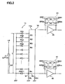
- FIG. 1 illustrates a structure of a level detector 10.
- the level detector 10 comprises: a light receiving element unit (a position detection device) 11; a first amplifier circuit (a first amplifier device) 20 configured to amplify a light receiving signal output from one terminal 11a of the light receiving element unit 11; a first gain switching circuit (a first gain switching device) 21 configured to switch and set a gain of the first amplifier circuit 20; a first peak hold circuit (a first peak hold device) 12 configured to hold a peak value of an amplified signal output from the first amplifier circuit 20; a second amplifier circuit (a second amplifier device) 30 configured to amplify the peak value held by the first peak hold circuit 12; a second gain switching circuit (a second gain switching device) 31 configured to switch and set a gain of the second amplifier circuit 30; a third amplifier circuit (a third amplifier device) 40 configured to amplify a light receiving signal output from another terminal 11b of the light receiving element unit 11; a third gain switching circuit (a third gain switching device) 41 configured to switch and set a
- the light receiving element unit 11 includes a plurality of light receiving elements PD1-PDn+1 which for example consist of photodiodes or the like.
- the plurality of light receiving elements PD1-PDn+1 are arranged in parallel with each other up and down (in vertical direction), and resistances R1-Rn are connected between anodes of the light receiving elements PD1-PDn+1 respectively.
- the anode of the light receiving element PD 1 is grounded through the resistance RH, and the anode of the light receiving element PDn+1 is grounded through the resistance RL.
- the first gain switching circuit 21 includes: a plurality of resistances 22R1-22Rm with different resistance values; and a plurality of switching circuits 22S1-22Sm connected in series with the resistances 22R1-22Rm respectively. Then a gain is switched by switching ON of the switching circuits 22S1-22Sm, and the gain is set according to the resistances 22R1-22Rm corresponding to the switching circuits 22S1-22Sm which is ON.
- the second gain switching circuit 31, the third gain switching circuit 41 and the fourth gain switching circuit 51 include the similar structures with the first gain switching circuit 21, therefore the explanation about these circuits are omitted.
- the arithmetic control device 60 includes a digital conversion circuit unit 61 which is configured to convert the peak value signals output from the second amplifier circuit 30 and the fourth amplifier circuit 50 to digital values; and an arithmetic analysis control unit 62 which is configured to analyze and detect a light receiving position of laser light received by the light receiving element unit 11, based on the digital values converted by the digital conversion circuit unit 61.
- the arithmetic control device 60 transmits gain controlling signals for turning on each of the switching circuits 22S1-52Sq of the first to the fourth gain switching circuits 21-51. Operations of the level detector 10 with such a structure will be described below.
- the light receiving position Lp a position irradiated by laser light (a light receiving position) is Lp, to detect the light receiving position effectively, it is preferable that such a condition ⁇ R»RH (RL) is satisfied, where ⁇ R being the summation of R1 to Rn.
- the light receiving position may be obtained by the following equation.
- Lp Vh - V ⁇ 1 / Vh + V ⁇ 1 ⁇ L ⁇ ⁇
- the light receiving element includes photodiode, and it is able to utilize PIN type photodiode when a high speed is required.
- the light receiving elements are arranged at equal spaces.
- the equally spaced arrangement is not necessary, a state similar with the equally spaced arrangement may be obtained by adjusting values of the resistances between the light receiving elements.
- it is not necessary to utilize the light receiving elements with similar performances for example area, amount of photoelectric conversion). In any event, it is easy to obtain the height position Lp by the ratio of the voltages Vh and Vl.
- the voltages Vh and Vl are amplified by the first amplifier circuit 20 and the third amplifier circuit 40 respectively.
- the gains of the first amplifier circuit 20 and the third amplifier circuit 40 are set respectively by the switching circuits (22S1 ⁇ 22Sm) and (42S1 ⁇ 42Sm) respectively which are turned on by the gain controlling signals output from the control device 60.
- Peak values of the voltages of the light receiving signals amplified by the first amplifier circuit 20 and the third amplifier circuit 40 are held by the first peak hold circuit 12 and the second peak hold circuit 13 respectively, and the held voltages of the light receiving signals are further amplified by the second amplifier circuit 30 and the fourth amplifier circuit 50.
- the first amplifier circuit 20 and the third amplifier circuit 40 amplify the voltages which are changed with time, so that it is unable to make the amplification degree large.
- the signals past the first peak hold circuit 12 and the second peak hold circuit 13 are held peak values, and the band (frequency band of input signals) is narrow, so that it is able to make the amplification degree of the second amplifier circuit 30 and the fourth amplifier circuit 50 large.
- simplified values are to be dealt with, so that in the arithmetic processing, the analysis is able to be performed easily.
- the gains of the second amplifier circuit 30 and the fourth amplifier circuit 50 are amplified by predetermined gains respectively, with predetermined switching circuits being turned on.
- the voltages of the light receiving signals amplified by the second amplifier circuit 30 and the fourth amplifier circuit 50 are converted to digital values by the digital conversion unit 61 of the arithmetic control device 60, and the arithmetic analysis control unit 62 analyzes and detects the light receiving position of laser light of the light receiving element unit 11, based on the digital values.
- the arithmetic control device 60 transmits the gain controlling signals to perform switching ON of the switching circuits 21 to 51 of the first to the fourth gain switching circuits and then the gains are switched, so that the voltages of the light receiving signals become proper values.
- the gains of the first amplifier circuit 20 and the third amplifier circuit 40 are set large, it is possible that the upper limits of the hold voltages of the first peak hold circuit 12 and the second peak hold circuit 13 are exceeded, therefore, by setting the gains of the first amplifier circuit 20 and the third amplifier circuit 40 to be low first, and then switching the gains of the second amplifier circuit 30 and the fourth amplifier circuit 50 to obtain proper signal voltages, consequently it is possible to analyze and obtain the light receiving position of laser light efficiently and rapidly.
- gains of the second gain switching circuit 31 and the fourth gain switching circuit 51 are two values for example 1 time and 5 times, and comparing signals output by the second and the fourth amplifier circuits 30, 50 when the gain is 1 time with signals output by the second and the fourth amplifier circuits 30, 50 when the gain is 5 times, determining if the signals are of proper largeness and then performing the analysis of the light receiving position, it is possible to analyze and obtain the light receiving position of laser light more efficiently and rapidly.
Landscapes
- Physics & Mathematics (AREA)
- Engineering & Computer Science (AREA)
- General Physics & Mathematics (AREA)
- Radar, Positioning & Navigation (AREA)
- Remote Sensing (AREA)
- Optical Radar Systems And Details Thereof (AREA)
- Length Measuring Devices By Optical Means (AREA)
- Optical Communication System (AREA)
Claims (2)
- Détecteur de niveau, comprenant :un dispositif de détection de position (11) comprenant une pluralité d'éléments de réception de lumière agencés parallèlement les uns aux autres ;un premier dispositif d'amplification (20) configuré pour amplifier un signal de réception de lumière délivré à partir d'une borne (11 a) du dispositif de détection de position (11) ;un premier dispositif de commutation de gain (21) connecté au premier dispositif d'amplification (20) et configuré pour commuter et fixer un gain du premier dispositif d'amplification (20) ;un premier dispositif de maintien de valeur crête (12) configuré pour maintenir une valeur crête d'un signal amplifié délivré par le premier dispositif d'amplification (20) ;un troisième dispositif d'amplification (40) configuré pour amplifier un signal de réception de lumière délivré à partir d'une autre borne (11 b) du dispositif de détection de position (11) ;un troisième dispositif de commutation de gain (41) connecté au troisième dispositif d'amplification (40) et configuré pour commuter et fixer un gain du troisième dispositif d'amplification (40) ;un deuxième dispositif de maintien de valeur crête (13) configuré pour maintenir une valeur crête d'une sortie amplifiée du troisième dispositif d'amplification (40) ;un dispositif de commande arithmétique (60) configuré pour analyser une position de réception de lumière de la lumière laser reçue par le dispositif de détection de position (11) ;un deuxième dispositif d'amplification (30) connecté au premier dispositif de maintien de valeur crête (12) et configuré pour amplifier la valeur crête maintenue par le premier dispositif de maintien de valeur crête (12) ;un deuxième dispositif de commutation de gain (31) connecté au deuxième dispositif d'amplification (30) et configuré pour commuter et fixer un gain du deuxième dispositif d'amplification (30) ;un quatrième dispositif d'ampüfication (50) connecté au deuxième dispositif de maintien de valeur crête (13) et configuré pour amplifier la valeur crête maintenue par le deuxième dispositif de maintien de valeur crête (13) ; etun quatrième dispositif de commutation de gain (51) connecté au quatrième dispositif d'amplification (50) et configuré pour commuter et fixer un gain du quatrième dispositif d'amplification (50) ;dans lequel le dispositif de commande arithmétique (60) est configuré pour analyser la position de réception de lumière de la lumière laser reçue par le dispositif de détection de position (11), sur la base de signaux délivrés par les premier à quatrième dispositifs d'amplification (20, 30, 40, 50), etdans lequel la commutation du premier dispositif de commutation de gain (21) et du deuxième dispositif de commutation de gain (31) est effectuée par un signal de commande provenant du dispositif de commande arithmétique (60).
- Détecteur de niveau selon la revendication 1, dans lequel, lorsque le signal appliqué au dispositif de commande arithmétique (60) est à l'extérieur d'une plage de détection, le dispositif de commande arithmétique (60) transmet le signal de commande au premier dispositif de commutation de gain (21) pour ajuster le signal amplifié du premier dispositif d'amplification (20), et transmet le signal de commande au deuxième dispositif de commutation de gain (31) pour ajuster le signal amplifié du deuxième dispositif d'amplification (30), par une procédure prédéterminée.
Applications Claiming Priority (1)
| Application Number | Priority Date | Filing Date | Title |
|---|---|---|---|
| JP2005304307A JP4912660B2 (ja) | 2005-10-19 | 2005-10-19 | レベル検出装置 |
Publications (3)
| Publication Number | Publication Date |
|---|---|
| EP1777496A2 EP1777496A2 (fr) | 2007-04-25 |
| EP1777496A3 EP1777496A3 (fr) | 2011-06-01 |
| EP1777496B1 true EP1777496B1 (fr) | 2014-11-05 |
Family
ID=37657609
Family Applications (1)
| Application Number | Title | Priority Date | Filing Date |
|---|---|---|---|
| EP06021852.6A Active EP1777496B1 (fr) | 2005-10-19 | 2006-10-18 | Détecteur de niveau |
Country Status (4)
| Country | Link |
|---|---|
| US (1) | US7339154B2 (fr) |
| EP (1) | EP1777496B1 (fr) |
| JP (1) | JP4912660B2 (fr) |
| CN (1) | CN1952600B (fr) |
Families Citing this family (7)
| Publication number | Priority date | Publication date | Assignee | Title |
|---|---|---|---|---|
| JP5128835B2 (ja) * | 2007-03-20 | 2013-01-23 | 株式会社トプコン | レーザ光受光位置検出センサ及びこれを用いたレベル装置 |
| EP2559967A1 (fr) | 2011-08-16 | 2013-02-20 | Leica Geosystems AG | Circuit de détection de lumière |
| CN103733025B (zh) | 2011-08-16 | 2017-09-29 | 莱卡地球系统公开股份有限公司 | 多psd布置和电路 |
| WO2014106074A1 (fr) * | 2012-12-29 | 2014-07-03 | Robert Bosch Gmbh | Niveau à laser rotatif et à détection laser |
| CN112414386B (zh) * | 2020-10-28 | 2022-07-01 | 武汉天宇光电仪器有限公司 | 一种数字化调平控制方法、控制器及控制系统 |
| EP4323722A4 (fr) | 2021-04-12 | 2025-03-05 | Milwaukee Electric Tool Corporation | Système de niveau laser à alignement de détecteur automatique |
| DE112022004570T5 (de) | 2021-12-29 | 2024-07-18 | Milwaukee Electric Tool Corporation | Lasernivellier mit innerer verstellbarer plattform |
Citations (2)
| Publication number | Priority date | Publication date | Assignee | Title |
|---|---|---|---|---|
| JPS61110002A (ja) * | 1984-11-02 | 1986-05-28 | Dainippon Printing Co Ltd | 光学濃度/網点面積率測定装置における自動レンジ制御方法 |
| US6462326B1 (en) * | 2000-05-08 | 2002-10-08 | The United States Of America As Represented By The Secretary Of The Air Force | Circuit for deriving the position of a fast pulsing laser on a silicon position sensing detector |
Family Cites Families (14)
| Publication number | Priority date | Publication date | Assignee | Title |
|---|---|---|---|---|
| US5177560A (en) * | 1991-11-06 | 1993-01-05 | Hewlett-Packard Company | Optical spectrum analyzer having adjustable sensitivity |
| US5206500A (en) * | 1992-05-28 | 1993-04-27 | Cincinnati Microwave, Inc. | Pulsed-laser detection with pulse stretcher and noise averaging |
| AU652513B2 (en) * | 1992-06-29 | 1994-08-25 | Nohmi Bosai Ltd | Smoke detecting apparatus for fire alarm |
| US5457310A (en) * | 1993-10-20 | 1995-10-10 | Varo Inc. | Method and system for automatically correcting boresight errors in a laser beam guidance system |
| JPH09196664A (ja) * | 1996-01-19 | 1997-07-31 | Seikosha Co Ltd | カメラ用測距装置 |
| JP3351946B2 (ja) * | 1996-01-30 | 2002-12-03 | 三洋電機株式会社 | 受光位置検出回路及びこれを用いた距離検出装置 |
| JP3827764B2 (ja) * | 1996-03-19 | 2006-09-27 | 株式会社トプコン | 建設機械用レーザー光検出表示装置 |
| US5952883A (en) * | 1996-10-25 | 1999-09-14 | Nec Corporation | Circuit arrangement for amplifying an electrical signal converted from an optical signal |
| US5923427A (en) * | 1997-07-10 | 1999-07-13 | Banner Engineering Corporation | Optical triangulation distance sensing system and method using a position sensitive detector and an automatic power controlled light source |
| JP3479835B2 (ja) * | 2000-09-13 | 2003-12-15 | 日本電気株式会社 | ベースバンド利得制御方法及びベースバンド利得制御回路 |
| JP2003347873A (ja) * | 2002-05-24 | 2003-12-05 | Hitachi Ltd | 多段アンプのゲイン制御方法及び装置 |
| JP4201180B2 (ja) | 2003-04-10 | 2008-12-24 | 株式会社ニコン・トリンブル | ビーム中心検出装置 |
| US6750953B1 (en) * | 2003-04-30 | 2004-06-15 | Trimble Navigation Limited | Position detecting laser receiver |
| US7265626B2 (en) * | 2005-12-20 | 2007-09-04 | Avago Technologies Ecbu Ip (Singapore) Pte. Ltd. | Fast-setting digital automatic gain control |
-
2005
- 2005-10-19 JP JP2005304307A patent/JP4912660B2/ja not_active Expired - Fee Related
-
2006
- 2006-10-18 CN CN2006101400789A patent/CN1952600B/zh not_active Expired - Fee Related
- 2006-10-18 US US11/583,655 patent/US7339154B2/en active Active
- 2006-10-18 EP EP06021852.6A patent/EP1777496B1/fr active Active
Patent Citations (2)
| Publication number | Priority date | Publication date | Assignee | Title |
|---|---|---|---|---|
| JPS61110002A (ja) * | 1984-11-02 | 1986-05-28 | Dainippon Printing Co Ltd | 光学濃度/網点面積率測定装置における自動レンジ制御方法 |
| US6462326B1 (en) * | 2000-05-08 | 2002-10-08 | The United States Of America As Represented By The Secretary Of The Air Force | Circuit for deriving the position of a fast pulsing laser on a silicon position sensing detector |
Also Published As
| Publication number | Publication date |
|---|---|
| JP4912660B2 (ja) | 2012-04-11 |
| US7339154B2 (en) | 2008-03-04 |
| CN1952600A (zh) | 2007-04-25 |
| US20070084988A1 (en) | 2007-04-19 |
| CN1952600B (zh) | 2010-11-17 |
| EP1777496A2 (fr) | 2007-04-25 |
| EP1777496A3 (fr) | 2011-06-01 |
| JP2007113999A (ja) | 2007-05-10 |
Similar Documents
| Publication | Publication Date | Title |
|---|---|---|
| US9576769B2 (en) | Weak signal detection system and electron microscope equipped with same | |
| US8797522B2 (en) | Light quantity detection method and device therefor | |
| US5471049A (en) | Light detecting apparatus having low noise automatic gain control circuit | |
| JP5889152B2 (ja) | 受光回路、レーザレーダ | |
| US6188473B1 (en) | Method and system for photodetection of photon-counting and current operation | |
| EP1777496B1 (fr) | Détecteur de niveau | |
| US20250093153A1 (en) | Laser Level System with Automatic Detector Alignment | |
| EP2910981A2 (fr) | Capteur photo-électrique | |
| EP3379224B1 (fr) | Dispositif de mesure de caractéristique optique | |
| JPH0212215A (ja) | カメラ用距離検出装置 | |
| JP4756614B2 (ja) | 信号検出装置 | |
| US10859495B2 (en) | Fluorescence sensing system | |
| JP2006180175A (ja) | 光電センサ | |
| EP1956340A1 (fr) | Capteur de niveau | |
| US9228891B2 (en) | Light to frequency converter optical sensor with electronic bias and adjustable gain | |
| JP4201180B2 (ja) | ビーム中心検出装置 | |
| JP6292759B2 (ja) | マークセンサ及び光検出素子によるマーク判定方法 | |
| US20150145539A1 (en) | Readout device, dual-function readout device, and detecting circuit thereof | |
| JP3165255B2 (ja) | 測距センサ | |
| JP2008203075A (ja) | 荷電粒子ビーム装置の吸収電流検出装置 | |
| JP2005207955A (ja) | 光検出用回路及び光検出器 | |
| JP2674468B2 (ja) | 距離検出装置 | |
| JP2918738B2 (ja) | 測距装置用光電変換回路 | |
| JP2018044838A (ja) | 測距装置 | |
| KR20030053732A (ko) | 대기 풍속 자동 측정장치 |
Legal Events
| Date | Code | Title | Description |
|---|---|---|---|
| PUAI | Public reference made under article 153(3) epc to a published international application that has entered the european phase |
Free format text: ORIGINAL CODE: 0009012 |
|
| 17P | Request for examination filed |
Effective date: 20061018 |
|
| AK | Designated contracting states |
Kind code of ref document: A2 Designated state(s): AT BE BG CH CY CZ DE DK EE ES FI FR GB GR HU IE IS IT LI LT LU LV MC NL PL PT RO SE SI SK TR |
|
| AX | Request for extension of the european patent |
Extension state: AL BA HR MK YU |
|
| PUAL | Search report despatched |
Free format text: ORIGINAL CODE: 0009013 |
|
| AK | Designated contracting states |
Kind code of ref document: A3 Designated state(s): AT BE BG CH CY CZ DE DK EE ES FI FR GB GR HU IE IS IT LI LT LU LV MC NL PL PT RO SE SI SK TR |
|
| AX | Request for extension of the european patent |
Extension state: AL BA HR MK RS |
|
| AKX | Designation fees paid |
Designated state(s): CH DE LI SE |
|
| 17Q | First examination report despatched |
Effective date: 20130410 |
|
| GRAP | Despatch of communication of intention to grant a patent |
Free format text: ORIGINAL CODE: EPIDOSNIGR1 |
|
| INTG | Intention to grant announced |
Effective date: 20140521 |
|
| GRAS | Grant fee paid |
Free format text: ORIGINAL CODE: EPIDOSNIGR3 |
|
| GRAA | (expected) grant |
Free format text: ORIGINAL CODE: 0009210 |
|
| RIN1 | Information on inventor provided before grant (corrected) |
Inventor name: KATAYAMA, YASUTAKA |
|
| AK | Designated contracting states |
Kind code of ref document: B1 Designated state(s): CH DE LI SE |
|
| REG | Reference to a national code |
Ref country code: CH Ref legal event code: EP |
|
| REG | Reference to a national code |
Ref country code: DE Ref legal event code: R096 Ref document number: 602006043554 Country of ref document: DE Effective date: 20141218 |
|
| REG | Reference to a national code |
Ref country code: CH Ref legal event code: NV Representative=s name: BRAUNPAT BRAUN EDER AG, CH |
|
| REG | Reference to a national code |
Ref country code: SE Ref legal event code: TRGR |
|
| REG | Reference to a national code |
Ref country code: DE Ref legal event code: R097 Ref document number: 602006043554 Country of ref document: DE |
|
| PLBE | No opposition filed within time limit |
Free format text: ORIGINAL CODE: 0009261 |
|
| STAA | Information on the status of an ep patent application or granted ep patent |
Free format text: STATUS: NO OPPOSITION FILED WITHIN TIME LIMIT |
|
| 26N | No opposition filed |
Effective date: 20150806 |
|
| PGFP | Annual fee paid to national office [announced via postgrant information from national office to epo] |
Ref country code: SE Payment date: 20151022 Year of fee payment: 10 |
|
| PG25 | Lapsed in a contracting state [announced via postgrant information from national office to epo] |
Ref country code: SE Free format text: LAPSE BECAUSE OF NON-PAYMENT OF DUE FEES Effective date: 20161019 |
|
| REG | Reference to a national code |
Ref country code: CH Ref legal event code: PCAR Free format text: NEW ADDRESS: HOLEESTRASSE 87, 4054 BASEL (CH) |
|
| PGFP | Annual fee paid to national office [announced via postgrant information from national office to epo] |
Ref country code: DE Payment date: 20230830 Year of fee payment: 18 Ref country code: CH Payment date: 20231102 Year of fee payment: 18 |
|
| REG | Reference to a national code |
Ref country code: DE Ref legal event code: R119 Ref document number: 602006043554 Country of ref document: DE |
|
| REG | Reference to a national code |
Ref country code: CH Ref legal event code: PL |
|
| PG25 | Lapsed in a contracting state [announced via postgrant information from national office to epo] |
Ref country code: DE Free format text: LAPSE BECAUSE OF NON-PAYMENT OF DUE FEES Effective date: 20250501 |
|
| PG25 | Lapsed in a contracting state [announced via postgrant information from national office to epo] |
Ref country code: CH Free format text: LAPSE BECAUSE OF NON-PAYMENT OF DUE FEES Effective date: 20241031 |