EP1783471A1 - Detecteur de distortion - Google Patents
Detecteur de distortion Download PDFInfo
- Publication number
- EP1783471A1 EP1783471A1 EP05788246A EP05788246A EP1783471A1 EP 1783471 A1 EP1783471 A1 EP 1783471A1 EP 05788246 A EP05788246 A EP 05788246A EP 05788246 A EP05788246 A EP 05788246A EP 1783471 A1 EP1783471 A1 EP 1783471A1
- Authority
- EP
- European Patent Office
- Prior art keywords
- substrate
- fixed member
- fixed
- strain
- resistance elements
- Prior art date
- Legal status (The legal status is an assumption and is not a legal conclusion. Google has not performed a legal analysis and makes no representation as to the accuracy of the status listed.)
- Granted
Links
Images


Classifications
-
- G—PHYSICS
- G01—MEASURING; TESTING
- G01L—MEASURING FORCE, STRESS, TORQUE, WORK, MECHANICAL POWER, MECHANICAL EFFICIENCY, OR FLUID PRESSURE
- G01L5/00—Apparatus for, or methods of, measuring force, work, mechanical power, or torque, specially adapted for specific purposes
- G01L5/04—Apparatus for, or methods of, measuring force, work, mechanical power, or torque, specially adapted for specific purposes for measuring tension in flexible members, e.g. ropes, cables, wires, threads, belts or bands
- G01L5/10—Apparatus for, or methods of, measuring force, work, mechanical power, or torque, specially adapted for specific purposes for measuring tension in flexible members, e.g. ropes, cables, wires, threads, belts or bands using electrical means
- G01L5/101—Apparatus for, or methods of, measuring force, work, mechanical power, or torque, specially adapted for specific purposes for measuring tension in flexible members, e.g. ropes, cables, wires, threads, belts or bands using electrical means using sensors inserted into the flexible member
-
- G—PHYSICS
- G01—MEASURING; TESTING
- G01L—MEASURING FORCE, STRESS, TORQUE, WORK, MECHANICAL POWER, MECHANICAL EFFICIENCY, OR FLUID PRESSURE
- G01L1/00—Measuring force or stress, in general
- G01L1/20—Measuring force or stress, in general by measuring variations in ohmic resistance of solid materials or of electrically-conductive fluids; by making use of electrokinetic cells, i.e. liquid-containing cells wherein an electrical potential is produced or varied upon the application of stress
- G01L1/22—Measuring force or stress, in general by measuring variations in ohmic resistance of solid materials or of electrically-conductive fluids; by making use of electrokinetic cells, i.e. liquid-containing cells wherein an electrical potential is produced or varied upon the application of stress using resistance strain gauges
- G01L1/2206—Special supports with preselected places to mount the resistance strain gauges; Mounting of supports
- G01L1/2231—Special supports with preselected places to mount the resistance strain gauges; Mounting of supports the supports being disc- or ring-shaped, adapted for measuring a force along a single direction
Definitions
- the present invention relates to a strain detector for detecting strain generated by applying a load.
- a conventional strain detector is disclosed in, for example, Japanese Patent Unexamined Publication No. H8-87375 .
- Fig. 12 is a bottom view showing a conventional strain detector
- Fig. 13 is a perspective view showing the strain detector
- Fig. 14 is a cross sectional view showing a state, in which the strain detector is mounted.
- Insulating substrate (hereinafter referred to as substrate) 1 includes an elastic member and an insulating layer formed on the surface thereof. Insulating substrate 1 is fixed to a lower surface of push member 2.
- Four strain resistance elements (hereinafter referred to as elements) 3 are provided on a lower surface of insulating substrate 1.
- Four strain resistance elements 3 are electrically connected to a pair of source electrodes 4, a pair of output electrodes 5, and a pair of earthed electrodes 6. Thereby, a bridge circuit is constituted.
- the strain detector is fixed to fixed member 7 by screws 8 in use.
- the push force When a push force is applied to an upper surface substantially centrally of insulating substrate 1 through push member 2, the push force generates bending moment on insulating substrate 1.
- the bending moment generates bending moment also on four elements 3 provided on the lower surface of insulating substrate 1.
- elements 3 are varied in value of resistance. Such variation in value of resistance is output from pair of output electrodes 5 to an external computer (not shown), and a push force applied to substrate 1 is calculated.
- substrate 1 is clamped and fixed to fixed member 7 by screws 8. Therefore, a fixed position is displaced when a shock is applied, so that a fixed length constructed as a beam is varied and the strain detector is degraded in characteristics such as sensitivity and 0-point voltage.
- the strain detector according to the invention includes a bridge circuit having at least two strain resistance elements, a substrate, a first fixed member, and a second fixed member.
- the substrate has a circuit portion electrically connected to the strain resistance elements.
- the strain resistance elements are arranged on the substrate.
- the first fixed member is fixed to a center of an area, where an outer periphery of the area is set at a position at which the strain resistance elements are arranged.
- the second fixed member is fixed outside the position, where the strain resistance elements are arranged, at the substrate.
- a center of an axis of the first fixed member, a center of an axis of the second fixed member, and the center of the area are positioned on a straight line, and the first fixed member and the second fixed member are arranged on two mutually opposed surfaces of the substrate.
- the first fixedmember and the second fixedmember form a beam on the substrate.
- a fixed position is not displaced even when a shock is applied, so that a fixed length constructed as a beam is not varied. Therefore, the strain detector is hard to vary in characteristics such as sensitivity and O-point voltage.
- Fig. 1 is a perspective view showing a strain detector according to Embodiment 1 of the invention
- Fig. 2 is an exploded perspective view showing the strain detector
- Figs. 3A to 3E are views illustrating a process of fabricating a substrate in the strain detector.
- first fixed member (hereinafter referred to as fixed member) 21 is fixed to a first surface which is an upper surface of substrate 11 made of stainless steel.
- Second fixed member (hereinafter referred to as fixed member) 31 is fixed to a lower surface which is a second surface opposed to the first surface in a position, in which an axis thereof corresponds to an axis of fixed member 21.
- Connector 41 is mounted to an end of substrate 11 to cover circuit portion 11N and to take out a signal.
- insulating layer 11A is formed on the first surface of substrate 11.
- wiring electrode 11B and strain resistance elements 11C are provided on insulating layer 11A.
- protective film 11D is laminated and formed on the strain resistance element. Strain resistance elements 11C are arranged on substrate 11 to be connected to circuit portion 11N.
- fixed member 21 includes columnar portion 21A and threaded portion 21B, a center of an axis of which substantially corresponds to a center of an axis of columnar portion 21A.
- Fixed member 31 includes ring-shaped convex portion 31A and threaded portion 31B, a center of an axis of which corresponds substantially to a center of an axis of convex portion 31A.
- Connector 41 is molded from, for example, a polybutylene terephthalate (PBT) resin, which contains glass fibers.
- Connector 41 includes at least frame 41C and three terminals 41A provided in frame 41C and is provided with mount holes 41B.
- insulating layer 11A is printed on the upper surface of substrate 11 shown in Fig. 3A to be baked.
- wiring electrode 11B is printed on insulating layer 11A to be baked.
- four strain resistance elements 11C are printed and baked so as to constitute a bridge circuit with the use of wiring electrode 11B.
- protective film 11D is printed and baked so as to cover a portion except a land portion for mounting of circuit parts such as IC, and connecting electrodes 11M.
- Protective film 11D is provided to protect the respective layers as printed and baked from moisture or the like.
- substrate 11 and fixed member 21 are fixed integrally so that a center of area 11E for fixation, on substrate 11 substantially corresponds to a center of an axis of fixed member 21.
- Fixed member 21 is fixed to a central portion of area 11E on an upper surface side. At this time, for example, laser is used to weld corner portions defined by area 11E and columnar portion 21A.
- Strain resistance elements 11C are arranged on an outer periphery of area 11E.
- fixed member 31 is arranged and fixed integrally in area 11G for fixation, on a lower surface side of substrate 11 so that an the center of axis of fixed member 21 corresponds to a center of an axis of fixed member 31.
- laser is used to weld area 11G and convex portion 31A.
- Fixed member 31 is fixed outside those positions on substrate 11, in which strain resistance elements 11C are arranged. In this manner, the center of an axis of fixed member 21, the center of an axis of fixed member 31, a center of area 11E are positioned on a straight line.
- Fixed member 21 and fixed member 31, respectively, are arranged on two mutually opposed surfaces of substrate 11. An outer periphery of columnar portion 21A of fixed member 21 and convex portion 31A of fixed member 31, which are fixed in this manner, constitute a beam on substrate 11.
- Connector 41 is fixed to hole 11H of substrate 11 through mount holes 41B by screws 51.
- Connecting electrodes 11M on substrate 11 are electrically joined to terminals 41A by soldering or the like.
- a silicon resin preferably covers an interior of frame 41C in order to protect circuit portion 11N.
- Fixed members 21, 31 may be arranged upside down on substrate 11. In this case, as shown in Fig. 4, it is necessary to provide notch portion 31C on fixed member 31 in a position facing circuit portion 11N in order to avoid interference with wiring electrode 11B provided on substrate 11 and protective film 11D. In a word, notch portion 31C prevents fixed member 31 from getting on wiring electrode 11B and protective film 11D.
- Substrate 11 and fixed members 21, 31 desirably correspond to each other in coefficient of thermal expansion. That is, fixed members 21, 31 are also preferably made of stainless steel. Thereby, welded portions of fixed members 21, 31 and substrate 11 are hard to break due to thermal expansion. IC may be provided on circuit portion 11N to correct variation of strain resistance elements 11C in value of resistance. By using this, accuracy in calculation of load (strain) is improved.
- fixed member 31 is mounted to a mount member (not shown) by threaded portion 31B.
- a beam which is provided on substrate 11, bends by an outer periphery of a bottom surface of columnar portion 21A and an inner periphery of convex portion 31A. Strain by such bending causes strain resistance elements 11C to vary in value of resistance. Since strain resistance elements 11C constitutes a bridge circuit with wiring electrode 11B, output is varied according to strain. In this manner, a load from a measuring object is obtained as a change in output. The change in output, which is thus obtained, is subjected to arithmetic processing by a processing circuit (not shown) to be converted into a load.
- fixed members 21, 31 are fixed integrally to substrate 11. Thereby, any displacement in the fixed position is not caused even when a shock is applied, so that a fixed length constructed as a beam is not varied. Thereby, the strain detector is hard to vary in characteristics such as sensitivity and O-point voltage, so that stable characteristics are maintained.
- a bridge circuit may be constituted by the use of at least two strain resistance elements 11C and a fixed resistance. Threaded portions 21B, 31B are not necessary in case of mounting fixed members 21, 31 to a mount member or a measuring object by other methods.
- Fig. 5 is an exploded perspective view showing a strain detector according to Embodiment 2 of the invention.
- the present embodiment is different from Embodiment 1 in that hole 11J is provided centrally of area 11E for fixation of substrate 11.
- Fixed member 21 is provided with threaded portion 21C at a bottom of columnar portion 21A.
- An inside diameter of hole 11J is larger than an outside diameter of threaded portion 21C but smaller than an outside diameter of columnar portion 21A.
- Fixed member 31 is provided with concave portion 31F inside convex portion 31A.
- Fastening member 61A for engaging with threaded portion 21C is fitted into concave portion 31F.
- the present embodiment is the same as Embodiment 1 except the matter described above.
- Threaded portion 21C is inserted through hole 11J and threaded portion 21C as inserted is clamped and fixed to substrate 11 by fastening member 61A. Thereafter, substrate 11 and fixed member 21 are fixed integrally so that an axis of fixed member 21 and a center of area 11E substantially correspond to each other. At this time, laser is used to weld a corner portion defined by area 11E and columnar portion 21A.
- Fixed member 31 is fixed integrally to substrate 11 so that fastening member 61A is accommodated (covered) by concave portion 31F. At this time, the fastening member is arranged so that a center of an axis of fixed member 21 and a center of an axis of fixed member 31 correspond to each other.
- This construction lessens a load on fixed member 21 in strength, and a fracture limit value in a fixed position in a case of applying a shock is increased.
- Clamping and fixation by fastening member 61A may be performed after welding. Looseness of fastening member 61A is prevented by integrally fixing fastening member 61A to substrate 11 by, for example, laser welding, so that the fracture limit value is increased.
- fixed members 21, 31 may be fixed and fixed member 21 may be clamped and fixed to substrate 11 by providing a female thread at a center of fixed member 31 and clamping threaded portion 21C to the female thread.
- fixed member 21 and substrate 11 may be fixed together by providing a female thread in place of hole 11J and clamping threaded portion 21C to the female thread.
- first fixed member 21 and fastening member are arranged upside down.
- Fixed member 21 is provided with flange portion 21D and threaded portion 21E.
- flange portion 21D of fixed member 21 and area 11G of substrate 11 are fixed together by, for example, laser welding.
- Threaded portion 21E is clamped and fixed to substrate 11 by fastening member 61B.
- Flange portion 21D is dimensioned to be accommodated in (covered by) concave portion 31F.
- Fig. 7 is an exploded perspective view showing a strain detector according to Embodiment 3 of the invention.
- Fig. 8 is a perspective view showing an arrangement of a substrate and a second fixed member in the strain detector shown in Fig. 7.
- insulating layer 11A formed on an upper surface (i.e., the first surface of substrate 11) or the like is omitted.
- the present embodiment is different from Embodiment 1 in that guide portions 31D are provided in two symmetrical locations on convex portion 31A of fixed member 31.
- the present embodiment is the same as Embodiment 1 except the matter described above.
- substrate 11 is inserted into guide portions 31D, and fixed member 31 and substrate 11 are fixed integrally by, for example, laser welding. With such construction, even when welds of fixed member 31 and substrate 11 are broken, fixed member 31 is held mechanically on substrate 11.
- guide portions 31D may be provided outside convex portion 31A instead of being provided on convex portion 31A of fixed member 31.
- Guide portions 31D may be not necessarily provided in two symmetrical locations on convex portion 31A. It suffices that guide portions 31D, into which substrate 11 is inserted, be provided on the side, where substrate 11 is fixed, of fixed member 31.
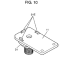
- Fig. 9 is an exploded perspective view showing a strain detector according to Embodiment 4 of the invention.
- Fig. 10 is a perspective view showing an arrangement of a substrate and a second fixed member in the strain detector shown in Fig. 9.
- insulating layer 11A formed on an upper surface (i.e., the first surface of substrate 11) or the like is omitted.
- the present embodiment is different from Embodiment 2 in that insertion holes 11K are provided on substrate 11 and hook portions 31E are provided on convex portion 31A of fixed member 31.
- the present embodiment is the same as Embodiment 2 except the matter described above.
- fixed member 31 By inserting hook portions 31E into insertion holes 11K and rotating it, fixed member 31 is suspended from substrate 11 as shown in Fig. 10. After fixed member 31 is thus assembled to substrate 11, it is fixed integrally to substrate 11 by, for example, laser welding. With such construction, even when welds of fixed member 31 and substrate 11 are broken, fixed member 31 is held mechanically on substrate 11.
- hook portions 31E may be provided outside convex portion 31A instead of being provided on convex portion 31A. That is, it suffices that the hook portions be provided on the side to be fixed to substrate 11.
- the construction may be applied to the construction of Embodiment 1.
- substrate 11 as welded and fixed member 21 agree substantially with each other in coefficient of thermal expansion.
- Fig. 11 is an exploded perspective view showing a strain detector according to Embodiment 5 of the invention.
- the present embodiment is different from Embodiment 1 in that mount 11L for fixed members 21, 31 at substrate 11 is formed to have the same external shape as that of fixedmember 31.
- fixed member 31 and mount 11L are configured to butt against each other at the time of, for example, laser welding, so that weld depth can be obtained efficiently. Therefore, fixed member 31 and substrate 11 are improved in weld strength, and a fracture limit value in a fixed position in a case of applying a shock is increased.
- the present construction may be applied to the construction of Embodiments 2 to 4.
- the strain detector With the strain detector according to the invention, a beam constructed at the time of assembly is hard to vary in length. Therefore, the strain detector is stable in characteristics and useful in application to a strain detector, in which accuracy in output signal is needed, or the like.
Landscapes
- Physics & Mathematics (AREA)
- General Physics & Mathematics (AREA)
- Chemical & Material Sciences (AREA)
- Analytical Chemistry (AREA)
- Measurement Of Force In General (AREA)
Applications Claiming Priority (2)
| Application Number | Priority Date | Filing Date | Title |
|---|---|---|---|
| JP2004292224A JP4779333B2 (ja) | 2004-10-05 | 2004-10-05 | 歪検出装置 |
| PCT/JP2005/018110 WO2006038553A1 (fr) | 2004-10-05 | 2005-09-30 | Detecteur de distortion |
Publications (3)
| Publication Number | Publication Date |
|---|---|
| EP1783471A1 true EP1783471A1 (fr) | 2007-05-09 |
| EP1783471A4 EP1783471A4 (fr) | 2010-07-07 |
| EP1783471B1 EP1783471B1 (fr) | 2015-12-09 |
Family
ID=36142628
Family Applications (1)
| Application Number | Title | Priority Date | Filing Date |
|---|---|---|---|
| EP05788246.6A Expired - Lifetime EP1783471B1 (fr) | 2004-10-05 | 2005-09-30 | Detecteur de distortion |
Country Status (5)
| Country | Link |
|---|---|
| US (1) | US7658118B2 (fr) |
| EP (1) | EP1783471B1 (fr) |
| JP (1) | JP4779333B2 (fr) |
| CN (1) | CN100582703C (fr) |
| WO (1) | WO2006038553A1 (fr) |
Families Citing this family (5)
| Publication number | Priority date | Publication date | Assignee | Title |
|---|---|---|---|---|
| JP4816157B2 (ja) * | 2005-05-19 | 2011-11-16 | パナソニック株式会社 | 歪検出装置 |
| JP4816158B2 (ja) * | 2005-05-19 | 2011-11-16 | パナソニック株式会社 | 歪検出装置 |
| WO2006123708A1 (fr) * | 2005-05-19 | 2006-11-23 | Matsushita Electric Industrial Co., Ltd. | Détecteur de contrainte |
| US9297687B2 (en) * | 2013-05-17 | 2016-03-29 | Sensata Technologies, Inc. | Sense element having a stud fitted within the sense element |
| JP6794293B2 (ja) | 2017-02-24 | 2020-12-02 | 日本電産コパル電子株式会社 | 起歪体およびその起歪体を備えた力覚センサ |
Family Cites Families (19)
| Publication number | Priority date | Publication date | Assignee | Title |
|---|---|---|---|---|
| US3915015A (en) * | 1974-03-18 | 1975-10-28 | Stanford Research Inst | Strain gauge transducer system |
| CA1259816A (fr) * | 1984-09-29 | 1989-09-26 | Kazuo Asakawa | Dispositif detecteur de forces |
| JPS6183929A (ja) * | 1984-09-29 | 1986-04-28 | Fujitsu Ltd | 力検出装置 |
| JP2584201B2 (ja) * | 1994-01-14 | 1997-02-26 | インターナショナル・ビジネス・マシーンズ・コーポレイション | 力変換器、コンピュータ・システムおよびキーボード |
| JP3243124B2 (ja) * | 1994-06-21 | 2002-01-07 | 本田技研工業株式会社 | 円輪板 |
| JPH0887375A (ja) * | 1994-09-16 | 1996-04-02 | Fujitsu Ltd | ポインティングデバイス |
| US5991676A (en) * | 1996-11-22 | 1999-11-23 | Breed Automotive Technology, Inc. | Seat occupant sensing system |
| JP3713391B2 (ja) * | 1998-10-12 | 2005-11-09 | アルプス電気株式会社 | 入力装置 |
| WO2002103367A1 (fr) * | 2001-06-18 | 2002-12-27 | Thomas P. Kicher & Co. | Transducteur d'acceleration et procede associe |
| US6578432B2 (en) * | 2001-06-19 | 2003-06-17 | Cts Corporation | Seat belt tension sensor |
| US20040145577A1 (en) * | 2001-07-27 | 2004-07-29 | Hiroshi Yajima | Input device and its manufacturing method |
| US6916997B2 (en) * | 2001-12-07 | 2005-07-12 | Robert Bosch Corporation | Weight sensors having centralized loose tolerance universal force and Mx/My moments overload stops |
| CA2366030A1 (fr) * | 2001-12-20 | 2003-06-20 | Global E Bang Inc. | Systeme de profilage |
| JP2002257655A (ja) * | 2002-03-06 | 2002-09-11 | Nitta Ind Corp | 静電容量式力センサー |
| JP2004069535A (ja) * | 2002-08-07 | 2004-03-04 | Matsushita Electric Ind Co Ltd | 歪センサ |
| JP2004152107A (ja) * | 2002-10-31 | 2004-05-27 | Alps Electric Co Ltd | 座標入力装置 |
| JP2004205410A (ja) * | 2002-12-26 | 2004-07-22 | Takata Corp | 荷重センサ及びシート重量計測装置 |
| US7255015B2 (en) * | 2003-07-31 | 2007-08-14 | Sensata Technologies, Inc. | Occupant weight sensor for vehicular seats, method for making and system therefor |
| US6969809B2 (en) * | 2003-09-22 | 2005-11-29 | Cts Corporation | Vehicle seat weight sensor |
-
2004
- 2004-10-05 JP JP2004292224A patent/JP4779333B2/ja not_active Expired - Fee Related
-
2005
- 2005-09-30 US US11/663,284 patent/US7658118B2/en not_active Expired - Fee Related
- 2005-09-30 EP EP05788246.6A patent/EP1783471B1/fr not_active Expired - Lifetime
- 2005-09-30 WO PCT/JP2005/018110 patent/WO2006038553A1/fr not_active Ceased
- 2005-09-30 CN CN200580034016A patent/CN100582703C/zh not_active Expired - Fee Related
Also Published As
| Publication number | Publication date |
|---|---|
| JP4779333B2 (ja) | 2011-09-28 |
| US7658118B2 (en) | 2010-02-09 |
| EP1783471B1 (fr) | 2015-12-09 |
| JP2006105758A (ja) | 2006-04-20 |
| CN101036040A (zh) | 2007-09-12 |
| WO2006038553A1 (fr) | 2006-04-13 |
| EP1783471A4 (fr) | 2010-07-07 |
| US20080245157A1 (en) | 2008-10-09 |
| CN100582703C (zh) | 2010-01-20 |
Similar Documents
| Publication | Publication Date | Title |
|---|---|---|
| JP5036764B2 (ja) | 電流センサー | |
| JP6964063B2 (ja) | センサアッシーおよび物理量測定装置 | |
| US8050055B2 (en) | Electronic apparatus | |
| JP5107779B2 (ja) | 電流センサ | |
| US20200182914A1 (en) | Current measuring device | |
| EP1783471B1 (fr) | Detecteur de distortion | |
| JP7063107B2 (ja) | 光コネクタケーブル及び金属部材 | |
| JP3440629B2 (ja) | 圧力センサ | |
| JPH11211749A (ja) | 半導体加速度センサ | |
| JPH11304606A (ja) | ロードセル | |
| JP2004069535A (ja) | 歪センサ | |
| CN110383024A (zh) | 力传感器 | |
| JP6999842B2 (ja) | 薄膜歪センサとそれを用いたトルクセンサ | |
| JPH01262431A (ja) | 力覚センサ | |
| JP2005106800A5 (fr) | ||
| JP2005106800A (ja) | 歪検出装置 | |
| JPH1114485A (ja) | 圧力センサ | |
| JP2011133314A (ja) | 電流センサの製造方法、及び、電流センサ | |
| US6021673A (en) | Semiconductor pressure detecting device | |
| JP6320064B2 (ja) | 加速度センサ | |
| JP2982679B2 (ja) | 圧力検出器 | |
| JP2001124648A (ja) | 圧力測定装置 | |
| JP2000304763A (ja) | 加速度センサユニット | |
| JPH10284973A (ja) | 気密端子 | |
| JPH0843433A (ja) | 加速度センサーとその製造方法 |
Legal Events
| Date | Code | Title | Description |
|---|---|---|---|
| PUAI | Public reference made under article 153(3) epc to a published international application that has entered the european phase |
Free format text: ORIGINAL CODE: 0009012 |
|
| 17P | Request for examination filed |
Effective date: 20070216 |
|
| AK | Designated contracting states |
Kind code of ref document: A1 Designated state(s): DE FR GB IT |
|
| DAX | Request for extension of the european patent (deleted) | ||
| RBV | Designated contracting states (corrected) |
Designated state(s): DE FR GB IT |
|
| RAP1 | Party data changed (applicant data changed or rights of an application transferred) |
Owner name: PANASONIC CORPORATION |
|
| A4 | Supplementary search report drawn up and despatched |
Effective date: 20100607 |
|
| RAP1 | Party data changed (applicant data changed or rights of an application transferred) |
Owner name: PANASONIC INTELLECTUAL PROPERTY MANAGEMENT CO., LT |
|
| RAP1 | Party data changed (applicant data changed or rights of an application transferred) |
Owner name: PANASONIC INTELLECTUAL PROPERTY MANAGEMENT CO., LT |
|
| REG | Reference to a national code |
Ref country code: DE Ref legal event code: R079 Ref document number: 602005048070 Country of ref document: DE Free format text: PREVIOUS MAIN CLASS: G01L0001220000 Ipc: G01L0005100000 |
|
| RIC1 | Information provided on ipc code assigned before grant |
Ipc: G01L 5/10 20060101AFI20150416BHEP Ipc: G01L 1/22 20060101ALI20150416BHEP |
|
| GRAJ | Information related to disapproval of communication of intention to grant by the applicant or resumption of examination proceedings by the epo deleted |
Free format text: ORIGINAL CODE: EPIDOSDIGR1 |
|
| GRAP | Despatch of communication of intention to grant a patent |
Free format text: ORIGINAL CODE: EPIDOSNIGR1 |
|
| INTG | Intention to grant announced |
Effective date: 20150630 |
|
| GRAS | Grant fee paid |
Free format text: ORIGINAL CODE: EPIDOSNIGR3 |
|
| GRAA | (expected) grant |
Free format text: ORIGINAL CODE: 0009210 |
|
| AK | Designated contracting states |
Kind code of ref document: B1 Designated state(s): DE FR GB IT |
|
| REG | Reference to a national code |
Ref country code: GB Ref legal event code: FG4D |
|
| REG | Reference to a national code |
Ref country code: DE Ref legal event code: R096 Ref document number: 602005048070 Country of ref document: DE |
|
| REG | Reference to a national code |
Ref country code: DE Ref legal event code: R097 Ref document number: 602005048070 Country of ref document: DE |
|
| PLBE | No opposition filed within time limit |
Free format text: ORIGINAL CODE: 0009261 |
|
| STAA | Information on the status of an ep patent application or granted ep patent |
Free format text: STATUS: NO OPPOSITION FILED WITHIN TIME LIMIT |
|
| 26N | No opposition filed |
Effective date: 20160912 |
|
| REG | Reference to a national code |
Ref country code: DE Ref legal event code: R119 Ref document number: 602005048070 Country of ref document: DE |
|
| GBPC | Gb: european patent ceased through non-payment of renewal fee |
Effective date: 20160930 |
|
| REG | Reference to a national code |
Ref country code: FR Ref legal event code: ST Effective date: 20170531 |
|
| PG25 | Lapsed in a contracting state [announced via postgrant information from national office to epo] |
Ref country code: GB Free format text: LAPSE BECAUSE OF NON-PAYMENT OF DUE FEES Effective date: 20160930 Ref country code: DE Free format text: LAPSE BECAUSE OF NON-PAYMENT OF DUE FEES Effective date: 20170401 Ref country code: FR Free format text: LAPSE BECAUSE OF NON-PAYMENT OF DUE FEES Effective date: 20160930 |
|
| PG25 | Lapsed in a contracting state [announced via postgrant information from national office to epo] |
Ref country code: IT Free format text: LAPSE BECAUSE OF NON-PAYMENT OF DUE FEES Effective date: 20160930 |