EP1783841A2 - Lichtemittierende Vorrichtung und deren Herstellung - Google Patents
Lichtemittierende Vorrichtung und deren Herstellung Download PDFInfo
- Publication number
- EP1783841A2 EP1783841A2 EP07003971A EP07003971A EP1783841A2 EP 1783841 A2 EP1783841 A2 EP 1783841A2 EP 07003971 A EP07003971 A EP 07003971A EP 07003971 A EP07003971 A EP 07003971A EP 1783841 A2 EP1783841 A2 EP 1783841A2
- Authority
- EP
- European Patent Office
- Prior art keywords
- light emitting
- film
- emitting structures
- devices
- etching
- Prior art date
- Legal status (The legal status is an assumption and is not a legal conclusion. Google has not performed a legal analysis and makes no representation as to the accuracy of the status listed.)
- Ceased
Links
Images






Classifications
-
- H—ELECTRICITY
- H10—SEMICONDUCTOR DEVICES; ELECTRIC SOLID-STATE DEVICES NOT OTHERWISE PROVIDED FOR
- H10H—INORGANIC LIGHT-EMITTING SEMICONDUCTOR DEVICES HAVING POTENTIAL BARRIERS
- H10H20/00—Individual inorganic light-emitting semiconductor devices having potential barriers, e.g. light-emitting diodes [LED]
- H10H20/01—Manufacture or treatment
- H10H20/011—Manufacture or treatment of bodies, e.g. forming semiconductor layers
- H10H20/018—Bonding of wafers
Definitions
- the present invention relates to light emitting devices and a method for fabricating the same.
- a light emitting device is fabricated by growing gallium nitride (GaN) crystals into a thin film.
- GaN gallium nitride
- the best choice of growing the GaN crystals is a GaN substrate.
- the GaN substrate is very expensive due to difficulty in growing GaN crystals, and the like.
- heterogeneous substrates include sapphire (A1203), silicone carbide (SiC), gallium arsenide (GaAs) and the like. Recently, a sapphire substrate among the heterogeneous substrates has been widely used.
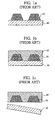
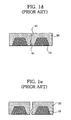
- FIGS. 1a to 1e are sectional views illustrating a conventional method for fabricating GaN-based light emitting devices. As shown in FIG. 1a, a plurality of light emitting structures (10) is formed on a sapphire substrate (20), each structure being spaced apart from one another.
- each of the plurality of light emitting structures (10) includes an active layer for generating light.
- a P-electrode is deposited on each of the plurality of light emitting structures such that the P-electrode is in ohmic contact therewith, thereby stably supplying an external current to the light emitting structure.
- a metallic film (30) is formed to wrap the plurality of light emitting structures (10) by means of plating or the like (FIG. 1b).
- the metallic film (30) holds the light emitting structures (10), the sapphire substrate (20) can be easily removed in a subsequent process.
- the sapphire substrate (20) is separated from each bottom of the light emitting structures (10) (FIG. 1c) .
- the sapphire substrate (20) may be removed using a laser lift off process.
- the laser lift off process is a process of separating and removing the sapphire substrate from the plurality of light emitting structures (10) wrapped by the metallic film (30), by irradiating a laser beam from below the sapphire substrate (20).
- a scribing process is performed to form a cutting groove (40) on the metallic film between adjacent light emitting structures (10), each structure spaced apart from each other.
- the rigidity of metal itself may cause a crack (41) under the cutting groove (40). Further, the crack (41) may propagate to the light emitting structures, resulting in degradation of the quality of light emitting devices.
- an expanding and breaking process is carried out, wherein a physical force is exerted on the adjacent light emitting structures wrapped by the metallic film (30) so as to individually divide the light emitting structures.
- the groove is formed on the metallic film to divide the light emitting structures and then used to perform the breaking process.
- a lower portion of the metallic film may not be cut occasionally, there is a problem in that all the light emitting structures cannot be completely divided.
- the metallic film is formed of a material with high ductility such as copper, the metallic film is easily stretched, causing difficulty in dividing the light emitting structures.
- An object of the present invention is to provide light emitting devices and a method for fabricating the same, wherein an etching film is removed to separate respective lateral surfaces of light emitting structures from one another, and a substrate is removed to separate lower portions of the devices from each other, further facilitating division of the devices.
- Another object of the present invention is to provide light emitting devices and a method for fabricating the same, wherein the devices are divided without carrying out a scribing process so that the occurrence of defects such as cracking or bending can be reduced, and spacing between the devices for the scribing process need not be maintained, thereby increasing the degree of integration of devices.
- a method for fabricating light emitting devices comprising: forming a plurality of light emitting structures on a heterogeneous substrate such that each structure is spaced apart from one another; forming an etching film out of a selectively etchable material between adjacent light emitting structures each spaced apart; forming a metallic film wrapping the plurality of light emitting structures and the etching film; separating the heterogeneous substrate from the plurality light emitting structures and the etching film wrapped by the metallic film; removing the etching film; and individually dividing the plurality of light emitting structures wrapped by the metallic film.
- a method for fabricating light emitting devices comprising: forming a plurality of light emitting structures on a heterogeneous substrate such that each structure is spaced apart from one another; forming an etching film, which has a height larger than that of each light emitting structure and is made of a selectively etchable material, between adjacent light emitting structures each spaced apart; forming a metallic film wrapping the plurality of light emitting structures and lateral surfaces of the etching film while exposing the top of the etching film; removing the etching film; and separating the heterogeneous substrate from the plurality light emitting structures wrapped by the metallic film.
- a method for fabricating light emitting devices comprising: forming a plurality of light emitting structures on a heterogeneous substrate such that the each structure is spaced apart from one another; forming an etching film, which is taller than each light emitting structure and is made of a selectively etchable material, between adjacent light emitting structures spaced apart from each other, the etching film; forming a metallic film wrapping the etching film and the plurality of light emitting structures; removing an upper portion of the metallic film to expose the top of the etching film; removing the etching film; and separating the heterogeneous substrate from the plurality light emitting structures wrapped by the metallic film.
- a method for fabricating light emitting devices comprising: forming a plurality of GaN-based light emitting structures on a heterogeneous substrate such that each structure is spaced apart from one another; forming an electrode on each of the plurality of GaN-based light emitting structures; forming an insulation film wrapping lateral surfaces of the plurality of GaN-based light emitting structures and lateral surfaces of the electrodes while isolating the plurality of GaN-based light emitting structures from one another; forming a seed layer wrapping the top of the electrode and an outer surface of the insulation film; forming an etching film out of a selectively etchable material on the seed layer between the spaced-apart GaN-based light emitting structures; forming a metallic film wrapping the top of the seed layer and the etching film; separating the heterogeneous substrate from the plurality of GaN-based light emitting structures; removing the etching film; and individually dividing the plurality of
- a light emitting device comprising: a light emitting structure including a first semiconductor layer with a first polarity, an active layer and a second semiconductor layer with a second polarity, which are sequentially stacked; a highly reflective film with an insulating property formed on lateral surfaces of the light emitting structure; a first electrode formed on the second semiconductor layer with the second polarity; and a second electrode formed under the first semiconductor layer with the first polarity.
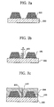
- a plurality of light emitting structures (100) is formed on a heterogeneous substrate (200) such that they are spaced apart from one another (FIG. 2a).
- each of the plurality of light emitting structures (100) includes an n-semiconductor layer (110a), an active layer (110b) and a p-semiconductor layer (110c), which are sequentially stacked as shown in FIG. 7.
- An insulation film (130) is formed on lateral surfaces of the n-semiconductor layer (110a), the active layer (110b) and the p-semiconductor (110c).
- the insulation film (130) is preferably a highly reflective film.
- a p-electrode be deposited on each of the plurality of light emitting structures (100) such that the p-electrode is in ohmic contact therewith.
- the heterogeneous substrate is preferably a sapphire substrate.
- an etching film (400) made of a material that can be selectively etched is formed between adjacent light emitting structures (100) spaced apart from each other.
- the material that can be selectively etched is preferably photo-resist or polyimide.
- the etching film (400) has a width of 5 to 50Dm and a height 5 to 100 ⁇ m.
- a metallic film (300) is formed to wrap the plurality of light emitting structures (100) and the etching film (400).
- the metallic film (300) is formed on the heterogeneous substrate (200) while wrapping the plurality of light emitting structures (100) and lateral surfaces and a portion of the top of the etching film (400).
- the metallic film (300) is not formed on a portion of the top of the etching film (400) so that an empty space (410) is formed above the etching film (400). That is, it is preferred that the metallic film (300) be divided by structures respectively, including the light emitting structures (100).
- the heterogeneous substrate (200) is separated from the plurality of light emitting structures (100) and the etching film (400) wrapped by the metallic film (300) (FIG. 2d).
- the separation of the heterogeneous substrate (200) is preferably made by performing a laser lift off process in which a laser beam is irradiated from below the heterogeneous substrate (200).
- the heterogeneous substrate (200) is separated from the light emitting structures (100), the metallic film (300) and the etching film (400). Thereafter, the etching film (400) is removed.
- the etching film (400) is preferably removed by means of etching using an organic solvent such as acetone, or using organic solvent spray.
- the removal of the etching film (400) provides an empty space 401 between adjacent light emitting structures (100).
- the etching film (400) existing between the plurality of light emitting structures (100) is removed to result in the empty space and the metallic film (300) is divided above the etching film (400), the metallic film can be easily divided with only a slight physical force into individual pieces of the metallic films respectively containing the light emitting structures (100).
- the division is achieved through an expanding and breaking process in which a physical force is applied while expanding the metallic film (300) so that the metallic film can be divided.
- an etching film (410) which has a height H2 taller than that H1 of the light emitting structures (100) and is made of a selectively etchable material, is formed between the plurality of light emitting structures (100) spaced apart from one another.
- a metallic film (300) is formed to expose the top of the etching film (410) and wrap the plurality of light emitting structures (100) and lateral surfaces of the etching film (410) (FIG. 3b). Thereafter, the etching film (410) is removed (FIG. 3c).
- an empty space (411) is formed between adjacent pieces of the metallic film (300), which wrap the respective light emitting structures (100), by means of the removal of the etching film (410).
- the plurality of light emitting structures (100) wrapped by the metallic film (300) are divided to fall within individual regions.
- heterogeneous substrate (200) is separated from the plurality of light emitting structures (100) wrapped by the metallic film (300) (FIG. 3d).
- the devices can be easily divided by removing the etching film (410) to separate the lateral side surfaces of the devices and subsequently removing the substrate to separate the bottom surfaces of the devices.
- an etching film is taller than each light emitting structure as compared with the process of FIG. 2b.
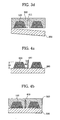
- An etching film (410) which has a height H2 taller than that H1 of the light emitting structures (100) and is made of a selectively etchable material, is formed between the plurality of light emitting structures (110) spaced apart from one another (FIG. 4a).
- a metallic film (300) is formed to wrap the etching film (410) and the plurality of light emitting structures (100) (FIG. 4b).
- heterogeneous substrate (200) is separated from the plurality of light emitting structures (100) wrapped by the metallic film (300) (FIG. 4e).
- the devices are divided by forming the metallic film to wrap the top of the etching film, removing the upper portion of the metallic film to expose the top of the etching film, and removing the etching film and the substrate.
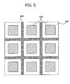
- FIG. 5 is a plan view showing an etching film formed between light emitting structures according to the present invention.
- Light emitting structures (100) each structure spaced apart from one another are formed on a heterogeneous substrate (200), and an etching film (400) is formed between the light emitting structures (100).
- the etching film (400) is formed in a grid pattern to separate respective lateral surfaces of the light emitting structures (100).
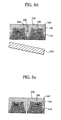
- a plurality of GaN-based light emitting structures (110) are formed on a heterogeneous substrate such that they are spaced apart from one another.
- An electrode (120) is formed on each of the GaN-based light emitting structures (110).
- Insulation films (130) are formed respectively to wrap lateral surfaces of the GaN-based light emitting structures (110) and lateral surfaces of the electrodes (120) and to isolate the plurality of GaN-based light emitting structures (110) from one another.
- a seed layer (140) is deposited to wrap the top of the electrode (120) and an entire outer surface of the insulation film (130).
- each of the plurality of GaN-based light emitting structures comprise a first semiconductor layer with a first polarity, an active layer, and a second semiconductor layer with a second polarity opposite to the first polarity. If the first polarity is an N-type, the second polarity is a P-type.
- the electrode (120) is preferably configured to be in ohmic contact with the p-semiconductor layer.
- the insulation film (130) may be formed of a highly reflective film with an insulating property. If such a highly reflective film wraps lateral surfaces of each of the light emitting structures (110), it reflects light emitted through the lateral surfaces of each of the light emitting structures (100), thereby improving light output.
- the seed layer (140) is used to allow a metal to be deposited thereon and is generally formed of a UBM (under bump metallization) layer.
- heterogeneous substrate (210) is preferably a sapphire (A1203) substrate.
- an etching film (450) is formed of a selectively etchable material on the seed layer (140) between adjacent GaN-based light emitting structures (110) each structure spaced apart from one another (FIG. 6b).
- the selectively etchable material preferably includes a photo-resist or a polyimide.
- the etching film (450) have a width of 5 to 50 ⁇ m and a height of 5 to 100 ⁇ m.
- a metallic film (310) is formed to wrap the top of the seed layer (140) and the etching film (450) (FIG. 6c).
- the metallic film (310) is preferably formed through a plating process.
- an incompletely bonded interface area (460) is formed from the top of the etching film (450) to the surface of the metallic film.
- the heterogeneous substrate (210) is separated from the plurality of GaN-based light emitting structures (110) (FIG. 6d).
- the separation of the heterogeneous substrate is preferably performed using a laser lift off process in which laser beam is irradiated from below the heterogeneous substrate. Thereafter, the etching film (450) is removed.
- the etching film (450) is removed by means of etching with an organic solvent such as acetone, or by using organic solvent spray.
- the removal of the etching film (450) provides an empty space (451) formed between adjacent GaN-based light emitting structures (100).
- the etching film (450) existing between the plurality of light emitting structures (100) is removed to result in the empty space and the metallic film (310) is divided above the etching film (450), the metallic film (130) and the seed layer (140) can be easily broken and divided with only a slight physical force into individual pieces of the metallic films (310) respectively containing the light emitting structures (100).
- the dividing process of FIG. 6e is performed using an expanding and breaking process.
- the thicknesses of the insulation film (130) and the seed layer (140), which are disposed under the etching layer (450), are small enough to be easily broken and thus do not disturb the division of the devices.
- FIG. 8 is a sectional view of a light emitting device according to the present invention.
- the light emitting device comprises a light emitting structure (170) having slant lateral side surfaces, and including a first semiconductor layer (171) with a first polarity, an active layer (172) and a second semiconductor layer (173) with a second polarity, which are stacked sequentially; a highly reflective film (180) with an insulating property formed on lateral side surfaces of the light emitting structure (170); a first electrode (350) wrapping and the second semiconductor layer (173) with a second polarity; and a second electrode (351) formed below the first semiconductor layer (171) with a first polarity.
- each lateral surface of the light emitting structure (170) is inclined at a certain angle ( ⁇ )
- light emitted from the active layer (172) is reflected on the highly reflective film (180) and passes through the first semiconductor layer (171) with the first polarity, resulting in an increased amount of light to be emitted downwardly of the light emitting structure (170).
- width of the first semiconductor layer (171) with a first polarity in the light emitting structure (170) is wider than that of the second semiconductor layer (173) with a second polarity.
- the light emitting structure (170) be tapered off as it goes from a lower end to an upper end thereof.
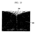
- FIG. 9 is an electron microscopic photograph showing a case where an etching film (500) is formed of photoresist between spaced-apart GaN-based light emitting structures, and a metallic film (600) made of copper is then plated thereon.
- an incompletely bonded interface area (510) is formed from the top of the etching film (500) to the surface of the metallic film (600).
- FIG. 10 is an enlarged photograph of the interface area (510) of FIG. 9.
- an etching film is removed to separate respective lateral surfaces of light emitting structures from one another, and a substrate is removed to separate lower portions of the devices from each other, thereby further facilitating division of the devices.
- the devices are divided without carrying out a scribing process so that the occurrence of defects such as cracking or bending can be reduced, and spacing between the devices for the scribing process need not be maintained, thereby increasing the degree of integration of devices.
Landscapes
- Led Devices (AREA)
Applications Claiming Priority (2)
| Application Number | Priority Date | Filing Date | Title |
|---|---|---|---|
| KR1020050060091A KR100606551B1 (ko) | 2005-07-05 | 2005-07-05 | 발광소자 제조방법 |
| EP06291110A EP1748499B1 (de) | 2005-07-05 | 2006-07-05 | Lichtemittierende Vorrichtung und deren Herstellung |
Related Parent Applications (1)
| Application Number | Title | Priority Date | Filing Date |
|---|---|---|---|
| EP06291110A Division EP1748499B1 (de) | 2005-07-05 | 2006-07-05 | Lichtemittierende Vorrichtung und deren Herstellung |
Publications (2)
| Publication Number | Publication Date |
|---|---|
| EP1783841A2 true EP1783841A2 (de) | 2007-05-09 |
| EP1783841A3 EP1783841A3 (de) | 2007-05-23 |
Family
ID=37074609
Family Applications (2)
| Application Number | Title | Priority Date | Filing Date |
|---|---|---|---|
| EP06291110A Ceased EP1748499B1 (de) | 2005-07-05 | 2006-07-05 | Lichtemittierende Vorrichtung und deren Herstellung |
| EP07003971A Ceased EP1783841A3 (de) | 2005-07-05 | 2006-07-05 | Lichtemittierende Vorrichtung und deren Herstellung |
Family Applications Before (1)
| Application Number | Title | Priority Date | Filing Date |
|---|---|---|---|
| EP06291110A Ceased EP1748499B1 (de) | 2005-07-05 | 2006-07-05 | Lichtemittierende Vorrichtung und deren Herstellung |
Country Status (6)
| Country | Link |
|---|---|
| US (1) | US7435606B2 (de) |
| EP (2) | EP1748499B1 (de) |
| JP (1) | JP5095143B2 (de) |
| KR (1) | KR100606551B1 (de) |
| CN (1) | CN100448043C (de) |
| DE (1) | DE602006005867D1 (de) |
Families Citing this family (21)
| Publication number | Priority date | Publication date | Assignee | Title |
|---|---|---|---|---|
| KR20070047114A (ko) * | 2005-11-01 | 2007-05-04 | 주식회사 엘지화학 | 플렉서블 기판을 구비한 소자의 제조방법 및 이에 의해제조된 플렉서블 기판을 구비한 소자 |
| KR100752717B1 (ko) | 2006-09-20 | 2007-08-29 | 삼성전기주식회사 | 수직구조 질화갈륨계 발광 다이오드 소자의 제조방법 |
| WO2009004980A1 (ja) * | 2007-06-29 | 2009-01-08 | Showa Denko K.K. | 発光ダイオードの製造方法 |
| DE102007043902A1 (de) | 2007-09-14 | 2009-03-19 | Osram Opto Semiconductors Gmbh | Verfahren zum Vereinzeln metallisierter Halbleiterbauelemente |
| JPWO2009119847A1 (ja) * | 2008-03-28 | 2011-07-28 | 京セラ株式会社 | 光学デバイスおよび光学デバイスの製造方法 |
| US10147843B2 (en) | 2008-07-24 | 2018-12-04 | Lumileds Llc | Semiconductor light emitting device including a window layer and a light-directing structure |
| US8236582B2 (en) | 2008-07-24 | 2012-08-07 | Philips Lumileds Lighting Company, Llc | Controlling edge emission in package-free LED die |
| DE102008049535A1 (de) * | 2008-09-29 | 2010-04-08 | Osram Opto Semiconductors Gmbh | LED-Modul und Herstellungsverfahren |
| JP4799606B2 (ja) * | 2008-12-08 | 2011-10-26 | 株式会社東芝 | 光半導体装置及び光半導体装置の製造方法 |
| JP4994401B2 (ja) | 2009-02-04 | 2012-08-08 | エンパイア テクノロジー ディベロップメント エルエルシー | 半導体デバイスの製造方法 |
| WO2011069242A1 (en) * | 2009-12-09 | 2011-06-16 | Cooledge Lighting Inc. | Semiconductor dice transfer-enabling apparatus and method for manufacturing transfer-enabling apparatus |
| US20110151588A1 (en) * | 2009-12-17 | 2011-06-23 | Cooledge Lighting, Inc. | Method and magnetic transfer stamp for transferring semiconductor dice using magnetic transfer printing techniques |
| US8334152B2 (en) * | 2009-12-18 | 2012-12-18 | Cooledge Lighting, Inc. | Method of manufacturing transferable elements incorporating radiation enabled lift off for allowing transfer from host substrate |
| US8652860B2 (en) | 2011-01-09 | 2014-02-18 | Bridgelux, Inc. | Packaging photon building blocks having only top side connections in a molded interconnect structure |
| US9461023B2 (en) * | 2011-10-28 | 2016-10-04 | Bridgelux, Inc. | Jetting a highly reflective layer onto an LED assembly |
| JP5985322B2 (ja) | 2012-03-23 | 2016-09-06 | 株式会社東芝 | 半導体発光装置及びその製造方法 |
| TWI528578B (zh) * | 2012-03-28 | 2016-04-01 | 鴻海精密工業股份有限公司 | 發光二極體製造方法 |
| US9608016B2 (en) | 2012-05-17 | 2017-03-28 | Koninklijke Philips N.V. | Method of separating a wafer of semiconductor devices |
| KR102301870B1 (ko) * | 2014-12-26 | 2021-09-15 | 쑤저우 레킨 세미컨덕터 컴퍼니 리미티드 | 발광 소자 및 발광 소자 패키지 |
| CN112582509B (zh) * | 2019-09-30 | 2022-07-08 | 成都辰显光电有限公司 | 微发光二极管芯片及显示面板 |
| KR20220068059A (ko) | 2020-11-18 | 2022-05-25 | 에스케이하이닉스 주식회사 | 반도체 메모리 장치 및 그 제조방법 |
Family Cites Families (24)
| Publication number | Priority date | Publication date | Assignee | Title |
|---|---|---|---|---|
| JPH01115174A (ja) * | 1987-10-28 | 1989-05-08 | Nec Corp | 発光ダイオードアレイ |
| JPH02251181A (ja) * | 1989-03-24 | 1990-10-08 | Oki Electric Ind Co Ltd | 発光ダイオード装置 |
| JP2720635B2 (ja) * | 1991-06-27 | 1998-03-04 | 日本電気株式会社 | 半導体発光素子の製造方法 |
| JPH06318731A (ja) * | 1993-03-12 | 1994-11-15 | Sharp Corp | 半導体発光装置 |
| JP3724834B2 (ja) * | 1995-03-09 | 2005-12-07 | 三菱電機株式会社 | 半導体レーザ装置の製造方法 |
| DE19629920B4 (de) * | 1995-08-10 | 2006-02-02 | LumiLeds Lighting, U.S., LLC, San Jose | Licht-emittierende Diode mit einem nicht-absorbierenden verteilten Braggreflektor |
| JPH10275936A (ja) | 1997-03-28 | 1998-10-13 | Rohm Co Ltd | 半導体発光素子の製法 |
| JPH11220165A (ja) | 1998-01-30 | 1999-08-10 | Toshiba Corp | 半導体発光素子の製造方法 |
| JP2000260760A (ja) | 1999-03-11 | 2000-09-22 | Toshiba Corp | ウェーハ及び半導体装置の製造方法 |
| US6355497B1 (en) * | 2000-01-18 | 2002-03-12 | Xerox Corporation | Removable large area, low defect density films for led and laser diode growth |
| US7053413B2 (en) * | 2000-10-23 | 2006-05-30 | General Electric Company | Homoepitaxial gallium-nitride-based light emitting device and method for producing |
| DE10221858A1 (de) * | 2002-02-25 | 2003-09-11 | Osram Opto Semiconductors Gmbh | Strahlungsemittierendes Halbleiterbauelement und Verfahren zur Herstellung desselben |
| US20030189215A1 (en) * | 2002-04-09 | 2003-10-09 | Jong-Lam Lee | Method of fabricating vertical structure leds |
| US6818532B2 (en) * | 2002-04-09 | 2004-11-16 | Oriol, Inc. | Method of etching substrates |
| US8294172B2 (en) * | 2002-04-09 | 2012-10-23 | Lg Electronics Inc. | Method of fabricating vertical devices using a metal support film |
| JP2004165226A (ja) * | 2002-11-08 | 2004-06-10 | Toyoda Gosei Co Ltd | Iii族窒化物系化合物半導体発光素子の製造方法 |
| DE10253911A1 (de) * | 2002-09-30 | 2004-04-08 | Osram Opto Semiconductors Gmbh | Strahlungsemittierendes Halbleiterbauelement und Verfahren zu dessen Herstellung |
| JP4143732B2 (ja) * | 2002-10-16 | 2008-09-03 | スタンレー電気株式会社 | 車載用波長変換素子 |
| JP4295669B2 (ja) * | 2003-05-22 | 2009-07-15 | パナソニック株式会社 | 半導体素子の製造方法 |
| US7019330B2 (en) * | 2003-08-28 | 2006-03-28 | Lumileds Lighting U.S., Llc | Resonant cavity light emitting device |
| JP4834951B2 (ja) * | 2003-09-29 | 2011-12-14 | ソニー株式会社 | Led素子形成方法 |
| US6884646B1 (en) * | 2004-03-10 | 2005-04-26 | Uni Light Technology Inc. | Method for forming an LED device with a metallic substrate |
| JP2007535804A (ja) * | 2004-03-15 | 2007-12-06 | ティンギ テクノロジーズ プライベート リミテッド | 半導体デバイスの製造 |
| US7064356B2 (en) * | 2004-04-16 | 2006-06-20 | Gelcore, Llc | Flip chip light emitting diode with micromesas and a conductive mesh |
-
2005
- 2005-07-05 KR KR1020050060091A patent/KR100606551B1/ko not_active Expired - Fee Related
-
2006
- 2006-07-05 EP EP06291110A patent/EP1748499B1/de not_active Ceased
- 2006-07-05 DE DE602006005867T patent/DE602006005867D1/de active Active
- 2006-07-05 EP EP07003971A patent/EP1783841A3/de not_active Ceased
- 2006-07-05 US US11/480,527 patent/US7435606B2/en active Active
- 2006-07-05 CN CNB200610103138XA patent/CN100448043C/zh active Active
- 2006-07-05 JP JP2006186054A patent/JP5095143B2/ja not_active Expired - Fee Related
Also Published As
| Publication number | Publication date |
|---|---|
| DE602006005867D1 (de) | 2009-05-07 |
| EP1748499A3 (de) | 2007-02-28 |
| JP2007019511A (ja) | 2007-01-25 |
| US7435606B2 (en) | 2008-10-14 |
| US20070020789A1 (en) | 2007-01-25 |
| KR100606551B1 (ko) | 2006-08-01 |
| EP1748499A2 (de) | 2007-01-31 |
| CN100448043C (zh) | 2008-12-31 |
| CN1933196A (zh) | 2007-03-21 |
| EP1783841A3 (de) | 2007-05-23 |
| JP5095143B2 (ja) | 2012-12-12 |
| EP1748499B1 (de) | 2009-03-25 |
Similar Documents
| Publication | Publication Date | Title |
|---|---|---|
| EP1748499B1 (de) | Lichtemittierende Vorrichtung und deren Herstellung | |
| US9012935B2 (en) | Vertically structured group III nitride semiconductor LED chip and method for manufacturing the same | |
| EP1662587B1 (de) | Licht emittierendes Bauelement und seine Herstellung | |
| KR100867541B1 (ko) | 수직형 발광 소자의 제조 방법 | |
| US9502603B2 (en) | Vertically structured group III nitride semiconductor LED chip and method for manufacturing the same | |
| US8587017B2 (en) | Light emitting device and method of fabricating a light emitting device | |
| JP5774712B2 (ja) | 半導体素子およびその製造方法 | |
| KR20070013273A (ko) | 반도체 장치의 제조 | |
| JP4940359B1 (ja) | 発光素子と発光素子および半導体素子の製造方法 | |
| EP2668674B1 (de) | Festkörperbeleuchtungsvorrichtungen mit kompakter grösse und herstellungsverfahren dafür | |
| EP2426741B1 (de) | Herstellungsverfahren für eine lichtemittierende Halbleitervorrichtung | |
| KR100978568B1 (ko) | 질화물 반도체 발광소자의 제조 방법 | |
| JPH11354841A (ja) | 半導体発光素子の製法 | |
| JP4542508B2 (ja) | 垂直型発光ダイオードおよびその製造方法 | |
| JP5723431B2 (ja) | Iii族窒化物半導体縦型構造ledチップ | |
| KR100657735B1 (ko) | 수직형 발광소자 제조방법 | |
| JP5763858B2 (ja) | Iii族窒化物半導体縦型構造ledチップの製造方法 |
Legal Events
| Date | Code | Title | Description |
|---|---|---|---|
| PUAI | Public reference made under article 153(3) epc to a published international application that has entered the european phase |
Free format text: ORIGINAL CODE: 0009012 |
|
| PUAL | Search report despatched |
Free format text: ORIGINAL CODE: 0009013 |
|
| AC | Divisional application: reference to earlier application |
Ref document number: 1748499 Country of ref document: EP Kind code of ref document: P |
|
| AK | Designated contracting states |
Kind code of ref document: A2 Designated state(s): AT BE BG CH CY CZ DE DK EE ES FI FR GB GR HU IE IS IT LI LT LU LV MC NL PL PT RO SE SI SK TR |
|
| AX | Request for extension of the european patent |
Extension state: AL BA HR MK YU |
|
| AK | Designated contracting states |
Kind code of ref document: A3 Designated state(s): AT BE BG CH CY CZ DE DK EE ES FI FR GB GR HU IE IS IT LI LT LU LV MC NL PL PT RO SE SI SK TR |
|
| AX | Request for extension of the european patent |
Extension state: AL BA HR MK YU |
|
| 17P | Request for examination filed |
Effective date: 20070910 |
|
| 17Q | First examination report despatched |
Effective date: 20071015 |
|
| AKX | Designation fees paid |
Designated state(s): DE FI GB NL |
|
| RAP1 | Party data changed (applicant data changed or rights of an application transferred) |
Owner name: LG INNOTEK CO., LTD. Owner name: LG ELECTRONICS, INC. |
|
| APBK | Appeal reference recorded |
Free format text: ORIGINAL CODE: EPIDOSNREFNE |
|
| APBN | Date of receipt of notice of appeal recorded |
Free format text: ORIGINAL CODE: EPIDOSNNOA2E |
|
| APBR | Date of receipt of statement of grounds of appeal recorded |
Free format text: ORIGINAL CODE: EPIDOSNNOA3E |
|
| APAF | Appeal reference modified |
Free format text: ORIGINAL CODE: EPIDOSCREFNE |
|
| RAP1 | Party data changed (applicant data changed or rights of an application transferred) |
Owner name: LG INNOTEK CO., LTD. Owner name: LG ELECTRONICS, INC. |
|
| RAP1 | Party data changed (applicant data changed or rights of an application transferred) |
Owner name: LG INNOTEK CO., LTD. Owner name: LG ELECTRONICS, INC. |
|
| APBT | Appeal procedure closed |
Free format text: ORIGINAL CODE: EPIDOSNNOA9E |
|
| STAA | Information on the status of an ep patent application or granted ep patent |
Free format text: STATUS: THE APPLICATION HAS BEEN REFUSED |
|
| 18R | Application refused |
Effective date: 20151006 |
|
| RIN1 | Information on inventor provided before grant (corrected) |
Inventor name: HA, JUNSEOK Inventor name: LEE, HYUNJAE |