EP1784065A1 - Substrat d'electrode - Google Patents
Substrat d'electrode Download PDFInfo
- Publication number
- EP1784065A1 EP1784065A1 EP05770814A EP05770814A EP1784065A1 EP 1784065 A1 EP1784065 A1 EP 1784065A1 EP 05770814 A EP05770814 A EP 05770814A EP 05770814 A EP05770814 A EP 05770814A EP 1784065 A1 EP1784065 A1 EP 1784065A1
- Authority
- EP
- European Patent Office
- Prior art keywords
- electrodes
- electrode
- wiring board
- substrate
- electronic
- Prior art date
- Legal status (The legal status is an assumption and is not a legal conclusion. Google has not performed a legal analysis and makes no representation as to the accuracy of the status listed.)
- Ceased
Links
Images






Classifications
-
- H—ELECTRICITY
- H05—ELECTRIC TECHNIQUES NOT OTHERWISE PROVIDED FOR
- H05K—PRINTED CIRCUITS; CASINGS OR CONSTRUCTIONAL DETAILS OF ELECTRIC APPARATUS; MANUFACTURE OF ASSEMBLAGES OF ELECTRICAL COMPONENTS
- H05K3/00—Apparatus or processes for manufacturing printed circuits
- H05K3/22—Secondary treatment of printed circuits
- H05K3/24—Reinforcing of the conductive pattern
- H05K3/243—Reinforcing of the conductive pattern characterised by selective plating, e.g. for finish plating of pads
-
- H—ELECTRICITY
- H10—SEMICONDUCTOR DEVICES; ELECTRIC SOLID-STATE DEVICES NOT OTHERWISE PROVIDED FOR
- H10W—GENERIC PACKAGES, INTERCONNECTIONS, CONNECTORS OR OTHER CONSTRUCTIONAL DETAILS OF DEVICES COVERED BY CLASS H10
- H10W70/00—Package substrates; Interposers; Redistribution layers [RDL]
- H10W70/01—Manufacture or treatment
- H10W70/05—Manufacture or treatment of insulating or insulated package substrates, or of interposers, or of redistribution layers
- H10W70/098—Applying pastes or inks, e.g. screen printing
-
- H—ELECTRICITY
- H10—SEMICONDUCTOR DEVICES; ELECTRIC SOLID-STATE DEVICES NOT OTHERWISE PROVIDED FOR
- H10W—GENERIC PACKAGES, INTERCONNECTIONS, CONNECTORS OR OTHER CONSTRUCTIONAL DETAILS OF DEVICES COVERED BY CLASS H10
- H10W70/00—Package substrates; Interposers; Redistribution layers [RDL]
- H10W70/60—Insulating or insulated package substrates; Interposers; Redistribution layers
-
- H—ELECTRICITY
- H10—SEMICONDUCTOR DEVICES; ELECTRIC SOLID-STATE DEVICES NOT OTHERWISE PROVIDED FOR
- H10W—GENERIC PACKAGES, INTERCONNECTIONS, CONNECTORS OR OTHER CONSTRUCTIONAL DETAILS OF DEVICES COVERED BY CLASS H10
- H10W70/00—Package substrates; Interposers; Redistribution layers [RDL]
- H10W70/60—Insulating or insulated package substrates; Interposers; Redistribution layers
- H10W70/67—Insulating or insulated package substrates; Interposers; Redistribution layers characterised by their insulating layers or insulating parts
- H10W70/69—Insulating materials thereof
-
- H—ELECTRICITY
- H10—SEMICONDUCTOR DEVICES; ELECTRIC SOLID-STATE DEVICES NOT OTHERWISE PROVIDED FOR
- H10W—GENERIC PACKAGES, INTERCONNECTIONS, CONNECTORS OR OTHER CONSTRUCTIONAL DETAILS OF DEVICES COVERED BY CLASS H10
- H10W74/00—Encapsulations, e.g. protective coatings
- H10W74/01—Manufacture or treatment
- H10W74/012—Manufacture or treatment of encapsulations on active surfaces of flip-chip devices, e.g. forming underfills
-
- H—ELECTRICITY
- H10—SEMICONDUCTOR DEVICES; ELECTRIC SOLID-STATE DEVICES NOT OTHERWISE PROVIDED FOR
- H10W—GENERIC PACKAGES, INTERCONNECTIONS, CONNECTORS OR OTHER CONSTRUCTIONAL DETAILS OF DEVICES COVERED BY CLASS H10
- H10W74/00—Encapsulations, e.g. protective coatings
- H10W74/10—Encapsulations, e.g. protective coatings characterised by their shape or disposition
- H10W74/15—Encapsulations, e.g. protective coatings characterised by their shape or disposition on active surfaces of flip-chip devices, e.g. underfills
-
- H—ELECTRICITY
- H05—ELECTRIC TECHNIQUES NOT OTHERWISE PROVIDED FOR
- H05K—PRINTED CIRCUITS; CASINGS OR CONSTRUCTIONAL DETAILS OF ELECTRIC APPARATUS; MANUFACTURE OF ASSEMBLAGES OF ELECTRICAL COMPONENTS
- H05K1/00—Printed circuits
- H05K1/02—Details
- H05K1/0266—Marks, test patterns or identification means
- H05K1/0268—Marks, test patterns or identification means for electrical inspection or testing
-
- H—ELECTRICITY
- H05—ELECTRIC TECHNIQUES NOT OTHERWISE PROVIDED FOR
- H05K—PRINTED CIRCUITS; CASINGS OR CONSTRUCTIONAL DETAILS OF ELECTRIC APPARATUS; MANUFACTURE OF ASSEMBLAGES OF ELECTRICAL COMPONENTS
- H05K2201/00—Indexing scheme relating to printed circuits covered by H05K1/00
- H05K2201/03—Conductive materials
- H05K2201/0332—Structure of the conductor
- H05K2201/0335—Layered conductors or foils
- H05K2201/0352—Differences between the conductors of different layers of a multilayer
-
- H—ELECTRICITY
- H05—ELECTRIC TECHNIQUES NOT OTHERWISE PROVIDED FOR
- H05K—PRINTED CIRCUITS; CASINGS OR CONSTRUCTIONAL DETAILS OF ELECTRIC APPARATUS; MANUFACTURE OF ASSEMBLAGES OF ELECTRICAL COMPONENTS
- H05K2201/00—Indexing scheme relating to printed circuits covered by H05K1/00
- H05K2201/03—Conductive materials
- H05K2201/0332—Structure of the conductor
- H05K2201/0388—Other aspects of conductors
- H05K2201/0391—Using different types of conductors
-
- H—ELECTRICITY
- H05—ELECTRIC TECHNIQUES NOT OTHERWISE PROVIDED FOR
- H05K—PRINTED CIRCUITS; CASINGS OR CONSTRUCTIONAL DETAILS OF ELECTRIC APPARATUS; MANUFACTURE OF ASSEMBLAGES OF ELECTRICAL COMPONENTS
- H05K2201/00—Indexing scheme relating to printed circuits covered by H05K1/00
- H05K2201/10—Details of components or other objects attached to or integrated in a printed circuit board
- H05K2201/10613—Details of electrical connections of non-printed components, e.g. special leads
- H05K2201/10621—Components characterised by their electrical contacts
- H05K2201/10674—Flip chip
-
- H—ELECTRICITY
- H05—ELECTRIC TECHNIQUES NOT OTHERWISE PROVIDED FOR
- H05K—PRINTED CIRCUITS; CASINGS OR CONSTRUCTIONAL DETAILS OF ELECTRIC APPARATUS; MANUFACTURE OF ASSEMBLAGES OF ELECTRICAL COMPONENTS
- H05K2203/00—Indexing scheme relating to apparatus or processes for manufacturing printed circuits covered by H05K3/00
- H05K2203/16—Inspection; Monitoring; Aligning
- H05K2203/162—Testing a finished product, e.g. heat cycle testing of solder joints
-
- H—ELECTRICITY
- H05—ELECTRIC TECHNIQUES NOT OTHERWISE PROVIDED FOR
- H05K—PRINTED CIRCUITS; CASINGS OR CONSTRUCTIONAL DETAILS OF ELECTRIC APPARATUS; MANUFACTURE OF ASSEMBLAGES OF ELECTRICAL COMPONENTS
- H05K3/00—Apparatus or processes for manufacturing printed circuits
- H05K3/22—Secondary treatment of printed circuits
- H05K3/28—Applying non-metallic protective coatings
- H05K3/282—Applying non-metallic protective coatings for inhibiting the corrosion of the circuit, e.g. for preserving the solderability
-
- H—ELECTRICITY
- H05—ELECTRIC TECHNIQUES NOT OTHERWISE PROVIDED FOR
- H05K—PRINTED CIRCUITS; CASINGS OR CONSTRUCTIONAL DETAILS OF ELECTRIC APPARATUS; MANUFACTURE OF ASSEMBLAGES OF ELECTRICAL COMPONENTS
- H05K3/00—Apparatus or processes for manufacturing printed circuits
- H05K3/30—Assembling printed circuits with electric components, e.g. with resistors
- H05K3/32—Assembling printed circuits with electric components, e.g. with resistors electrically connecting electric components or wires to printed circuits
- H05K3/328—Assembling printed circuits with electric components, e.g. with resistors electrically connecting electric components or wires to printed circuits by welding
-
- H—ELECTRICITY
- H05—ELECTRIC TECHNIQUES NOT OTHERWISE PROVIDED FOR
- H05K—PRINTED CIRCUITS; CASINGS OR CONSTRUCTIONAL DETAILS OF ELECTRIC APPARATUS; MANUFACTURE OF ASSEMBLAGES OF ELECTRICAL COMPONENTS
- H05K3/00—Apparatus or processes for manufacturing printed circuits
- H05K3/30—Assembling printed circuits with electric components, e.g. with resistors
- H05K3/32—Assembling printed circuits with electric components, e.g. with resistors electrically connecting electric components or wires to printed circuits
- H05K3/34—Assembling printed circuits with electric components, e.g. with resistors electrically connecting electric components or wires to printed circuits by soldering
- H05K3/341—Surface mounted components
-
- H—ELECTRICITY
- H10—SEMICONDUCTOR DEVICES; ELECTRIC SOLID-STATE DEVICES NOT OTHERWISE PROVIDED FOR
- H10W—GENERIC PACKAGES, INTERCONNECTIONS, CONNECTORS OR OTHER CONSTRUCTIONAL DETAILS OF DEVICES COVERED BY CLASS H10
- H10W72/00—Interconnections or connectors in packages
- H10W72/01—Manufacture or treatment
- H10W72/012—Manufacture or treatment of bump connectors, dummy bumps or thermal bumps
- H10W72/01251—Changing the shapes of bumps
- H10W72/01255—Changing the shapes of bumps by using masks
-
- H—ELECTRICITY
- H10—SEMICONDUCTOR DEVICES; ELECTRIC SOLID-STATE DEVICES NOT OTHERWISE PROVIDED FOR
- H10W—GENERIC PACKAGES, INTERCONNECTIONS, CONNECTORS OR OTHER CONSTRUCTIONAL DETAILS OF DEVICES COVERED BY CLASS H10
- H10W72/00—Interconnections or connectors in packages
- H10W72/071—Connecting or disconnecting
- H10W72/072—Connecting or disconnecting of bump connectors
-
- H—ELECTRICITY
- H10—SEMICONDUCTOR DEVICES; ELECTRIC SOLID-STATE DEVICES NOT OTHERWISE PROVIDED FOR
- H10W—GENERIC PACKAGES, INTERCONNECTIONS, CONNECTORS OR OTHER CONSTRUCTIONAL DETAILS OF DEVICES COVERED BY CLASS H10
- H10W72/00—Interconnections or connectors in packages
- H10W72/071—Connecting or disconnecting
- H10W72/072—Connecting or disconnecting of bump connectors
- H10W72/07211—Treating the bond pad before connecting, e.g. by applying flux or cleaning
-
- H—ELECTRICITY
- H10—SEMICONDUCTOR DEVICES; ELECTRIC SOLID-STATE DEVICES NOT OTHERWISE PROVIDED FOR
- H10W—GENERIC PACKAGES, INTERCONNECTIONS, CONNECTORS OR OTHER CONSTRUCTIONAL DETAILS OF DEVICES COVERED BY CLASS H10
- H10W72/00—Interconnections or connectors in packages
- H10W72/071—Connecting or disconnecting
- H10W72/072—Connecting or disconnecting of bump connectors
- H10W72/07231—Techniques
- H10W72/07234—Using a reflow oven
-
- H—ELECTRICITY
- H10—SEMICONDUCTOR DEVICES; ELECTRIC SOLID-STATE DEVICES NOT OTHERWISE PROVIDED FOR
- H10W—GENERIC PACKAGES, INTERCONNECTIONS, CONNECTORS OR OTHER CONSTRUCTIONAL DETAILS OF DEVICES COVERED BY CLASS H10
- H10W72/00—Interconnections or connectors in packages
- H10W72/071—Connecting or disconnecting
- H10W72/072—Connecting or disconnecting of bump connectors
- H10W72/07231—Techniques
- H10W72/07236—Soldering or alloying
-
- H—ELECTRICITY
- H10—SEMICONDUCTOR DEVICES; ELECTRIC SOLID-STATE DEVICES NOT OTHERWISE PROVIDED FOR
- H10W—GENERIC PACKAGES, INTERCONNECTIONS, CONNECTORS OR OTHER CONSTRUCTIONAL DETAILS OF DEVICES COVERED BY CLASS H10
- H10W72/00—Interconnections or connectors in packages
- H10W72/071—Connecting or disconnecting
- H10W72/073—Connecting or disconnecting of die-attach connectors
-
- H—ELECTRICITY
- H10—SEMICONDUCTOR DEVICES; ELECTRIC SOLID-STATE DEVICES NOT OTHERWISE PROVIDED FOR
- H10W—GENERIC PACKAGES, INTERCONNECTIONS, CONNECTORS OR OTHER CONSTRUCTIONAL DETAILS OF DEVICES COVERED BY CLASS H10
- H10W72/00—Interconnections or connectors in packages
- H10W72/20—Bump connectors, e.g. solder bumps or copper pillars; Dummy bumps; Thermal bumps
- H10W72/241—Dispositions, e.g. layouts
-
- H—ELECTRICITY
- H10—SEMICONDUCTOR DEVICES; ELECTRIC SOLID-STATE DEVICES NOT OTHERWISE PROVIDED FOR
- H10W—GENERIC PACKAGES, INTERCONNECTIONS, CONNECTORS OR OTHER CONSTRUCTIONAL DETAILS OF DEVICES COVERED BY CLASS H10
- H10W72/00—Interconnections or connectors in packages
- H10W72/20—Bump connectors, e.g. solder bumps or copper pillars; Dummy bumps; Thermal bumps
- H10W72/251—Materials
- H10W72/252—Materials comprising solid metals or solid metalloids, e.g. PbSn, Ag or Cu
-
- H—ELECTRICITY
- H10—SEMICONDUCTOR DEVICES; ELECTRIC SOLID-STATE DEVICES NOT OTHERWISE PROVIDED FOR
- H10W—GENERIC PACKAGES, INTERCONNECTIONS, CONNECTORS OR OTHER CONSTRUCTIONAL DETAILS OF DEVICES COVERED BY CLASS H10
- H10W72/00—Interconnections or connectors in packages
- H10W72/20—Bump connectors, e.g. solder bumps or copper pillars; Dummy bumps; Thermal bumps
- H10W72/29—Bond pads specially adapted therefor
-
- H—ELECTRICITY
- H10—SEMICONDUCTOR DEVICES; ELECTRIC SOLID-STATE DEVICES NOT OTHERWISE PROVIDED FOR
- H10W—GENERIC PACKAGES, INTERCONNECTIONS, CONNECTORS OR OTHER CONSTRUCTIONAL DETAILS OF DEVICES COVERED BY CLASS H10
- H10W72/00—Interconnections or connectors in packages
- H10W72/50—Bond wires
- H10W72/531—Shapes of wire connectors
- H10W72/536—Shapes of wire connectors the connected ends being ball-shaped
-
- H—ELECTRICITY
- H10—SEMICONDUCTOR DEVICES; ELECTRIC SOLID-STATE DEVICES NOT OTHERWISE PROVIDED FOR
- H10W—GENERIC PACKAGES, INTERCONNECTIONS, CONNECTORS OR OTHER CONSTRUCTIONAL DETAILS OF DEVICES COVERED BY CLASS H10
- H10W72/00—Interconnections or connectors in packages
- H10W72/50—Bond wires
- H10W72/531—Shapes of wire connectors
- H10W72/5363—Shapes of wire connectors the connected ends being wedge-shaped
-
- H—ELECTRICITY
- H10—SEMICONDUCTOR DEVICES; ELECTRIC SOLID-STATE DEVICES NOT OTHERWISE PROVIDED FOR
- H10W—GENERIC PACKAGES, INTERCONNECTIONS, CONNECTORS OR OTHER CONSTRUCTIONAL DETAILS OF DEVICES COVERED BY CLASS H10
- H10W72/00—Interconnections or connectors in packages
- H10W72/50—Bond wires
- H10W72/551—Materials of bond wires
- H10W72/552—Materials of bond wires comprising metals or metalloids, e.g. silver
- H10W72/5522—Materials of bond wires comprising metals or metalloids, e.g. silver comprising gold [Au]
-
- H—ELECTRICITY
- H10—SEMICONDUCTOR DEVICES; ELECTRIC SOLID-STATE DEVICES NOT OTHERWISE PROVIDED FOR
- H10W—GENERIC PACKAGES, INTERCONNECTIONS, CONNECTORS OR OTHER CONSTRUCTIONAL DETAILS OF DEVICES COVERED BY CLASS H10
- H10W72/00—Interconnections or connectors in packages
- H10W72/50—Bond wires
- H10W72/551—Materials of bond wires
- H10W72/552—Materials of bond wires comprising metals or metalloids, e.g. silver
- H10W72/5525—Materials of bond wires comprising metals or metalloids, e.g. silver comprising copper [Cu]
-
- H—ELECTRICITY
- H10—SEMICONDUCTOR DEVICES; ELECTRIC SOLID-STATE DEVICES NOT OTHERWISE PROVIDED FOR
- H10W—GENERIC PACKAGES, INTERCONNECTIONS, CONNECTORS OR OTHER CONSTRUCTIONAL DETAILS OF DEVICES COVERED BY CLASS H10
- H10W72/00—Interconnections or connectors in packages
- H10W72/50—Bond wires
- H10W72/59—Bond pads specially adapted therefor
-
- H—ELECTRICITY
- H10—SEMICONDUCTOR DEVICES; ELECTRIC SOLID-STATE DEVICES NOT OTHERWISE PROVIDED FOR
- H10W—GENERIC PACKAGES, INTERCONNECTIONS, CONNECTORS OR OTHER CONSTRUCTIONAL DETAILS OF DEVICES COVERED BY CLASS H10
- H10W72/00—Interconnections or connectors in packages
- H10W72/851—Dispositions of multiple connectors or interconnections
- H10W72/853—On the same surface
- H10W72/856—Bump connectors and die-attach connectors
-
- H—ELECTRICITY
- H10—SEMICONDUCTOR DEVICES; ELECTRIC SOLID-STATE DEVICES NOT OTHERWISE PROVIDED FOR
- H10W—GENERIC PACKAGES, INTERCONNECTIONS, CONNECTORS OR OTHER CONSTRUCTIONAL DETAILS OF DEVICES COVERED BY CLASS H10
- H10W72/00—Interconnections or connectors in packages
- H10W72/851—Dispositions of multiple connectors or interconnections
- H10W72/874—On different surfaces
- H10W72/884—Die-attach connectors and bond wires
-
- H—ELECTRICITY
- H10—SEMICONDUCTOR DEVICES; ELECTRIC SOLID-STATE DEVICES NOT OTHERWISE PROVIDED FOR
- H10W—GENERIC PACKAGES, INTERCONNECTIONS, CONNECTORS OR OTHER CONSTRUCTIONAL DETAILS OF DEVICES COVERED BY CLASS H10
- H10W72/00—Interconnections or connectors in packages
- H10W72/90—Bond pads, in general
- H10W72/951—Materials of bond pads
- H10W72/952—Materials of bond pads comprising metals or metalloids, e.g. PbSn, Ag or Cu
-
- H—ELECTRICITY
- H10—SEMICONDUCTOR DEVICES; ELECTRIC SOLID-STATE DEVICES NOT OTHERWISE PROVIDED FOR
- H10W—GENERIC PACKAGES, INTERCONNECTIONS, CONNECTORS OR OTHER CONSTRUCTIONAL DETAILS OF DEVICES COVERED BY CLASS H10
- H10W74/00—Encapsulations, e.g. protective coatings
-
- H—ELECTRICITY
- H10—SEMICONDUCTOR DEVICES; ELECTRIC SOLID-STATE DEVICES NOT OTHERWISE PROVIDED FOR
- H10W—GENERIC PACKAGES, INTERCONNECTIONS, CONNECTORS OR OTHER CONSTRUCTIONAL DETAILS OF DEVICES COVERED BY CLASS H10
- H10W90/00—Package configurations
- H10W90/701—Package configurations characterised by the relative positions of pads or connectors relative to package parts
- H10W90/721—Package configurations characterised by the relative positions of pads or connectors relative to package parts of bump connectors
- H10W90/724—Package configurations characterised by the relative positions of pads or connectors relative to package parts of bump connectors between a chip and a stacked insulating package substrate, interposer or RDL
-
- H—ELECTRICITY
- H10—SEMICONDUCTOR DEVICES; ELECTRIC SOLID-STATE DEVICES NOT OTHERWISE PROVIDED FOR
- H10W—GENERIC PACKAGES, INTERCONNECTIONS, CONNECTORS OR OTHER CONSTRUCTIONAL DETAILS OF DEVICES COVERED BY CLASS H10
- H10W90/00—Package configurations
- H10W90/701—Package configurations characterised by the relative positions of pads or connectors relative to package parts
- H10W90/731—Package configurations characterised by the relative positions of pads or connectors relative to package parts of die-attach connectors
- H10W90/734—Package configurations characterised by the relative positions of pads or connectors relative to package parts of die-attach connectors between a chip and a stacked insulating package substrate, interposer or RDL
-
- H—ELECTRICITY
- H10—SEMICONDUCTOR DEVICES; ELECTRIC SOLID-STATE DEVICES NOT OTHERWISE PROVIDED FOR
- H10W—GENERIC PACKAGES, INTERCONNECTIONS, CONNECTORS OR OTHER CONSTRUCTIONAL DETAILS OF DEVICES COVERED BY CLASS H10
- H10W90/00—Package configurations
- H10W90/701—Package configurations characterised by the relative positions of pads or connectors relative to package parts
- H10W90/731—Package configurations characterised by the relative positions of pads or connectors relative to package parts of die-attach connectors
- H10W90/736—Package configurations characterised by the relative positions of pads or connectors relative to package parts of die-attach connectors between a chip and a stacked lead frame, conducting package substrate or heat sink
-
- H—ELECTRICITY
- H10—SEMICONDUCTOR DEVICES; ELECTRIC SOLID-STATE DEVICES NOT OTHERWISE PROVIDED FOR
- H10W—GENERIC PACKAGES, INTERCONNECTIONS, CONNECTORS OR OTHER CONSTRUCTIONAL DETAILS OF DEVICES COVERED BY CLASS H10
- H10W90/00—Package configurations
- H10W90/701—Package configurations characterised by the relative positions of pads or connectors relative to package parts
- H10W90/751—Package configurations characterised by the relative positions of pads or connectors relative to package parts of bond wires
- H10W90/754—Package configurations characterised by the relative positions of pads or connectors relative to package parts of bond wires between a chip and a stacked insulating package substrate, interposer or RDL
-
- H—ELECTRICITY
- H10—SEMICONDUCTOR DEVICES; ELECTRIC SOLID-STATE DEVICES NOT OTHERWISE PROVIDED FOR
- H10W—GENERIC PACKAGES, INTERCONNECTIONS, CONNECTORS OR OTHER CONSTRUCTIONAL DETAILS OF DEVICES COVERED BY CLASS H10
- H10W90/00—Package configurations
- H10W90/701—Package configurations characterised by the relative positions of pads or connectors relative to package parts
- H10W90/751—Package configurations characterised by the relative positions of pads or connectors relative to package parts of bond wires
- H10W90/756—Package configurations characterised by the relative positions of pads or connectors relative to package parts of bond wires between a chip and a stacked lead frame, conducting package substrate or heat sink
Definitions
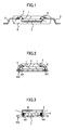
- FIG. 1 is a schematic structural view of a related art Quad Flat Package (QFP) as an IC chip.
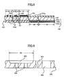
- FIG. 2 is a schematic structural view of a related art electronic circuit board manufactured by an old type Chip On Board (COB) process wherein a bare chip 2 as an IC ship is connected to a wiring board by wire bonding.
- FIG. 3 is a schematic structural view of a related art electronic circuit board manufactured by a new type Chip On Board (COB) process wherein the bare chip is mounted as a flip chip.
- COB Chip On Board
- the lead electrodes 3 project from a side surface of the package 4 in the shape of gull wings.
- the lead electrodes 3 lead electric input or output of the bare chip 2 provided in the package 4 to a wiring board not shown in FIG. 1.
- Such mounting of the bare chip 2 is done by a Surface Mount technology (SMT).
- SMT Surface Mount technology
- a solder paste lump is printed on the electrode 101 of the wiring board 100 by a mask printing method.
- a chip such as an IC chip or chip condenser is mounted on the wiring board 100 so that an electrode pad 1 formed on a lower surface of the chip part comes in contact with the printed solder paste lump.
- solder particles in the solder paste lump are melted then made solid, so that the electrode 101 of the wiring board 100 and the electrode pad of the chip are connected by the solder 6.
- the bare chip 2 is mounted on the wiring board without providing the wire used for the wired bonding. Under this structure, it is possible to make the mounting area smaller because the wire 5 is not provided to the outside of the bare chip 2.
- a gap is formed between the lower surface of the bare chip 2 and the surface of the wiring board 100.
- Such a gap is filled with an underfill material 7.
- An inventor of the present invention determined that the educed amount of gold against the solder 6 becomes smaller by reducing the thickness of the Au surface layer of the electrode 101.
- the thickness of the Au surface layer may be approximately 2 ⁇ m, it is not possible to prevent the solder 6 from becoming fragile.
- electroless plating since the thickness of the Au surface layer may be approximately several hundreds nm, it is possible to sufficiently prevent the solder 6 from becoming fragile.
- a wiring board including: a substrate made of an insulation material and wired by a conductive material; wherein a plurality of electrodes is formed on a surface of the substrate; and a non-Au electrode not having an Au surface layer and an Au electrode having the Au surface layer are formed as the electrodes.
- an electronic circuit board including: a wiring board where a plurality of electrodes is formed on a surface of a substrate which substrate is made of an insulation material and wired by a conductive material; and a plurality of electronic parts having contact electrodes configured to connect to the electrodes formed on the surface of the substrate, the electronic parts being surface-mounted on the wiring board; wherein the wiring board includes non-Au electrodes not having Au surface layers and Au electrodes having the Au surface layers as the electrodes; at least one of the electronic parts has the Au electrode having the Au surface layer as the contact electrode; the Au surface layer has a flat contact surface having an area greater than the area of a side surface of the Au surface layer; and the contact surface is soldered to the non-Au electrode of the wiring board.
- FIG. 6 is a plan view seen from a first surface side of a Printed Wiring Board (PWB) 150.
- PWB Printed Wiring Board
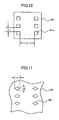
- plan areas of the non-Au electrodes 151 formed in at least the flip chip mounting area R3 are less than 0.049 mm 2 and all of the Au electrodes 152 have plan areas equal to or greater than 0.049 mm 2 .
- plan areas of the non-Au electrodes 151 formed in the flip chip mounting area R3 less than 0.049 mm 2 , it can be used for mounting a small size flip chip.
- all of the Au electrodes 152 having the plan areas equal to or greater than 0.049 mm 2 oxidation of all of the electrodes formed on the second surface of the substrate 153 can be prevented by the Au surface layer 152c.
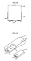
- the underfill material 502 jetted from the inclination part may come in contact with both the flip chip 301 and the module board 210.
- the underfill material 502 becomes solid based on evaporation of the solvent.
- All of or a part of the non-Au electrodes may have plan areas less than 0.049 mm 2 , and all of the Au electrodes may have plan areas equal to or greater than 0.049 mm 2 .
- the flip chip 301 is mounted on the PWB 150 so that the solder paste lumps 203 and the contact electrodes 301d are stacked.
- the present invention can be applied to a wiring board such as a printed wiring board where plural electrodes are formed on a surface of a substrate made of an insulation material for mounting an electronic part such as IC chip or a condenser, an electronic circuit board, an electronic apparatus and a manufacturing method of the electronic circuit board.
- a wiring board such as a printed wiring board where plural electrodes are formed on a surface of a substrate made of an insulation material for mounting an electronic part such as IC chip or a condenser, an electronic circuit board, an electronic apparatus and a manufacturing method of the electronic circuit board.
Landscapes
- Engineering & Computer Science (AREA)
- Manufacturing & Machinery (AREA)
- Microelectronics & Electronic Packaging (AREA)
- Electric Connection Of Electric Components To Printed Circuits (AREA)
- Wire Bonding (AREA)
- Parts Printed On Printed Circuit Boards (AREA)
- Non-Metallic Protective Coatings For Printed Circuits (AREA)
- Structures For Mounting Electric Components On Printed Circuit Boards (AREA)
Applications Claiming Priority (4)
| Application Number | Priority Date | Filing Date | Title |
|---|---|---|---|
| JP2004235448 | 2004-08-12 | ||
| JP2004235438 | 2004-08-12 | ||
| JP2005215800A JP2006080493A (ja) | 2004-08-12 | 2005-07-26 | 電極基板 |
| PCT/JP2005/014748 WO2006016650A1 (fr) | 2004-08-12 | 2005-08-11 | Substrat d’électrode |
Publications (2)
| Publication Number | Publication Date |
|---|---|
| EP1784065A1 true EP1784065A1 (fr) | 2007-05-09 |
| EP1784065A4 EP1784065A4 (fr) | 2009-07-22 |
Family
ID=35839410
Family Applications (1)
| Application Number | Title | Priority Date | Filing Date |
|---|---|---|---|
| EP05770814A Ceased EP1784065A4 (fr) | 2004-08-12 | 2005-08-11 | Substrat d'electrode |
Country Status (5)
| Country | Link |
|---|---|
| US (1) | US7732935B2 (fr) |
| EP (1) | EP1784065A4 (fr) |
| JP (1) | JP2006080493A (fr) |
| CN (1) | CN101023717B (fr) |
| WO (1) | WO2006016650A1 (fr) |
Families Citing this family (8)
| Publication number | Priority date | Publication date | Assignee | Title |
|---|---|---|---|---|
| KR100874588B1 (ko) * | 2007-09-05 | 2008-12-16 | 성균관대학교산학협력단 | 전기적 특성 평가가 가능한 플립칩 및 이것의 제조 방법 |
| USRE48422E1 (en) * | 2007-09-05 | 2021-02-02 | Research & Business Foundation Sungkyunkwan Univ. | Method of making flip chip |
| CN102646606B (zh) * | 2011-02-16 | 2014-12-24 | 中电智能卡有限责任公司 | Ic卡模块的封装方法 |
| JP6045436B2 (ja) * | 2013-05-02 | 2016-12-14 | ルネサスエレクトロニクス株式会社 | 電子装置 |
| US9425157B2 (en) | 2014-02-26 | 2016-08-23 | Taiwan Semiconductor Manufacturing Company Limited | Substrate and package structure |
| CN104308314A (zh) * | 2014-10-11 | 2015-01-28 | 昆山圆裕电子科技有限公司 | Dip通孔零件的回流焊接工艺 |
| JP6889399B2 (ja) * | 2017-08-08 | 2021-06-18 | 大日本印刷株式会社 | 貫通電極基板 |
| CN113921404A (zh) * | 2021-09-24 | 2022-01-11 | 青岛歌尔微电子研究院有限公司 | 一种系统级封装结构的封装方法 |
Family Cites Families (30)
| Publication number | Priority date | Publication date | Assignee | Title |
|---|---|---|---|---|
| US3394527A (en) * | 1967-07-24 | 1968-07-30 | American Cyanamid Co | Reinforcing anisotropic non-homogeneous engineering structures |
| JPS58192351A (ja) | 1982-05-06 | 1983-11-09 | Sharp Corp | 半導体装置の製造方法 |
| JPH02296336A (ja) | 1989-05-10 | 1990-12-06 | Seiko Epson Corp | 半導体回路バンプの製造方法 |
| JPH05167236A (ja) * | 1991-12-19 | 1993-07-02 | Sumitomo Bakelite Co Ltd | 回路等への半田付け方法 |
| JPH07193166A (ja) * | 1993-11-19 | 1995-07-28 | Citizen Watch Co Ltd | 半田バンプ付き半導体装置及びその製造方法 |
| FI940953A7 (fi) * | 1994-02-28 | 1995-08-29 | Optatech Oy | Polymeerikalvot ja menetelmä niiden valmistamiseksi |
| US6524644B1 (en) * | 1999-08-26 | 2003-02-25 | Enthone Inc. | Process for selective deposition of OSP coating on copper, excluding deposition on gold |
| US6534192B1 (en) * | 1999-09-24 | 2003-03-18 | Lucent Technologies Inc. | Multi-purpose finish for printed wiring boards and method of manufacture of such boards |
| JP3952434B2 (ja) | 2000-03-29 | 2007-08-01 | ローム株式会社 | 電池パックおよびその製造方法 |
| DE10018025A1 (de) * | 2000-04-04 | 2001-10-18 | Atotech Deutschland Gmbh | Verfahren zum Erzeugen von lötfähigen Oberflächen und funktionellen Oberflächen auf Schaltungsträgern |
| JP3855592B2 (ja) | 2000-04-19 | 2006-12-13 | 松下電器産業株式会社 | 小型モジュールの製造方法 |
| JP3477656B2 (ja) * | 2000-06-21 | 2003-12-10 | 三洋ジ−エスソフトエナジー株式会社 | 電池の外部端子とそれを用いた電池パック |
| TW511257B (en) * | 2000-12-11 | 2002-11-21 | Chino Excel Technology Corp | Flip-chip mounting method for decreasing conducting resistance in power transistor of charging battery protection circuit |
| US6494361B1 (en) * | 2001-01-26 | 2002-12-17 | Amkor Technology, Inc. | Semiconductor module package substrate fabrication method |
| US6515744B2 (en) * | 2001-02-08 | 2003-02-04 | Therma-Wave, Inc. | Small spot ellipsometer |
| JP3792129B2 (ja) * | 2001-03-01 | 2006-07-05 | 新光電気工業株式会社 | キャパシタ、キャパシタ内蔵回路基板及びそれらの製造方法 |
| US6744135B2 (en) * | 2001-05-22 | 2004-06-01 | Hitachi, Ltd. | Electronic apparatus |
| JP2002368038A (ja) * | 2001-06-07 | 2002-12-20 | Fuji Electric Co Ltd | フリップチップ実装方法 |
| JP3866591B2 (ja) | 2001-10-29 | 2007-01-10 | 富士通株式会社 | 電極間接続構造体の形成方法および電極間接続構造体 |
| US7130198B2 (en) * | 2001-12-06 | 2006-10-31 | Rohm Co., Ltd. | Resin-packaged protection circuit module for rechargeable batteries and method of making the same |
| JP3872995B2 (ja) | 2002-03-20 | 2007-01-24 | Tdk株式会社 | ベアチップ実装方法 |
| JP2003318308A (ja) * | 2002-04-18 | 2003-11-07 | Nippon Mektron Ltd | 可撓性回路基板のフリップチップic接続用回路パターン |
| JP2004165637A (ja) * | 2002-10-21 | 2004-06-10 | Matsushita Electric Ind Co Ltd | 半導体装置 |
| JP2004171964A (ja) * | 2002-11-20 | 2004-06-17 | Sony Corp | 回路基板、電池の接続方法、並びに電源装置 |
| CN100405881C (zh) * | 2003-03-18 | 2008-07-23 | 日本特殊陶业株式会社 | 接线板 |
| US7141874B2 (en) * | 2003-05-14 | 2006-11-28 | Matsushita Electric Industrial Co., Ltd. | Electronic component packaging structure and method for producing the same |
| JP4033811B2 (ja) | 2003-06-19 | 2008-01-16 | 株式会社リコー | フリップチップ実装体 |
| US7186645B2 (en) * | 2003-10-13 | 2007-03-06 | Intel Corporation | Selective plating of package terminals |
| WO2005069486A1 (fr) * | 2004-01-19 | 2005-07-28 | Murata Manufacturing Co., Ltd. | Dispositif a onde limite acoustique |
| JP4736451B2 (ja) * | 2005-02-03 | 2011-07-27 | パナソニック株式会社 | 多層配線基板とその製造方法、および多層配線基板を用いた半導体パッケージと電子機器 |
-
2005
- 2005-07-26 JP JP2005215800A patent/JP2006080493A/ja active Pending
- 2005-08-11 WO PCT/JP2005/014748 patent/WO2006016650A1/fr not_active Ceased
- 2005-08-11 EP EP05770814A patent/EP1784065A4/fr not_active Ceased
- 2005-08-11 CN CN2005800266184A patent/CN101023717B/zh not_active Expired - Fee Related
-
2006
- 2006-04-20 US US11/408,123 patent/US7732935B2/en not_active Expired - Fee Related
Also Published As
| Publication number | Publication date |
|---|---|
| CN101023717A (zh) | 2007-08-22 |
| US7732935B2 (en) | 2010-06-08 |
| EP1784065A4 (fr) | 2009-07-22 |
| JP2006080493A (ja) | 2006-03-23 |
| WO2006016650A1 (fr) | 2006-02-16 |
| CN101023717B (zh) | 2010-05-05 |
| US20060214297A1 (en) | 2006-09-28 |
Similar Documents
| Publication | Publication Date | Title |
|---|---|---|
| JP3565047B2 (ja) | 半田バンプの形成方法および半田バンプの実装方法 | |
| KR20080017431A (ko) | 프린트 배선판 및 프린트 배선판의 제조 방법 | |
| EP0889512A2 (fr) | Procédé de commande de la forme et de la hauteur d'une bosse de brasure | |
| JP2002208668A (ja) | 半導体装置およびその製造方法 | |
| US7732935B2 (en) | Wiring board, electronic circuit board, electronic apparatus and manufacturing method of electronic circuit board | |
| JP2018137276A (ja) | プリント回路板およびその製造方法、並びに電子機器 | |
| KR100432325B1 (ko) | 전극형성방법 및 그에 이용되는 범프 전극 피형성체 | |
| US6402012B1 (en) | Method for forming solder bumps using a solder jetting device | |
| JP2000040713A (ja) | 半導体パッケージの製造方法 | |
| JP2004200539A (ja) | 部品の接続端子及び電子機器 | |
| JP4159631B2 (ja) | 半導体パッケージの製造方法 | |
| JP2017130697A (ja) | 厚銅配線基板 | |
| JP2000151086A (ja) | プリント回路ユニット及びその製造方法 | |
| JPH11345826A (ja) | 半導体装置、半導体装置の製造方法及び半導体装置の実装方法 | |
| JP3582286B2 (ja) | 配線基板の製造方法 | |
| KR100746365B1 (ko) | 플립칩 실장용 기판의 제조방법 | |
| CN1450612A (zh) | 在单面柔性基板背面形成凸点的方法 | |
| JP3493999B2 (ja) | 半田バンプの形成方法および半田バンプの実装方法 | |
| JP2751897B2 (ja) | ボールグリッドアレイ実装構造及び実装方法 | |
| JP2526796B2 (ja) | テ―プキャリアパッケ―ジ | |
| JPH11150151A (ja) | 集積回路チップの実装構造および方法 | |
| JPH02165633A (ja) | 半導体装置の製造方法 | |
| JP2006093178A (ja) | 電子機器の製造方法 | |
| JPH11307215A (ja) | 半田付けされる端子を具備する電子部品の面実装方法、及びその面実装構造 | |
| US20070148950A1 (en) | Object and bonding method thereof |
Legal Events
| Date | Code | Title | Description |
|---|---|---|---|
| PUAI | Public reference made under article 153(3) epc to a published international application that has entered the european phase |
Free format text: ORIGINAL CODE: 0009012 |
|
| 17P | Request for examination filed |
Effective date: 20070117 |
|
| AK | Designated contracting states |
Kind code of ref document: A1 Designated state(s): DE FR GB |
|
| DAX | Request for extension of the european patent (deleted) | ||
| RBV | Designated contracting states (corrected) |
Designated state(s): DE FR GB |
|
| A4 | Supplementary search report drawn up and despatched |
Effective date: 20090618 |
|
| 17Q | First examination report despatched |
Effective date: 20130409 |
|
| REG | Reference to a national code |
Ref country code: DE Ref legal event code: R003 |
|
| STAA | Information on the status of an ep patent application or granted ep patent |
Free format text: STATUS: THE APPLICATION HAS BEEN REFUSED |
|
| 18R | Application refused |
Effective date: 20171008 |