EP1789849B1 - Verwendung von methanofullerenderivaten als resistmaterialien und verfahren zur bildung einer resistschicht - Google Patents
Verwendung von methanofullerenderivaten als resistmaterialien und verfahren zur bildung einer resistschicht Download PDFInfo
- Publication number
- EP1789849B1 EP1789849B1 EP05783725A EP05783725A EP1789849B1 EP 1789849 B1 EP1789849 B1 EP 1789849B1 EP 05783725 A EP05783725 A EP 05783725A EP 05783725 A EP05783725 A EP 05783725A EP 1789849 B1 EP1789849 B1 EP 1789849B1
- Authority
- EP
- European Patent Office
- Prior art keywords
- methanofullerene
- resist
- derivatives
- addend
- coating layer
- Prior art date
- Legal status (The legal status is an assumption and is not a legal conclusion. Google has not performed a legal analysis and makes no representation as to the accuracy of the status listed.)
- Expired - Lifetime
Links
Images


Classifications
-
- B—PERFORMING OPERATIONS; TRANSPORTING
- B82—NANOTECHNOLOGY
- B82Y—SPECIFIC USES OR APPLICATIONS OF NANOSTRUCTURES; MEASUREMENT OR ANALYSIS OF NANOSTRUCTURES; MANUFACTURE OR TREATMENT OF NANOSTRUCTURES
- B82Y30/00—Nanotechnology for materials or surface science, e.g. nanocomposites
-
- G—PHYSICS
- G03—PHOTOGRAPHY; CINEMATOGRAPHY; ANALOGOUS TECHNIQUES USING WAVES OTHER THAN OPTICAL WAVES; ELECTROGRAPHY; HOLOGRAPHY
- G03F—PHOTOMECHANICAL PRODUCTION OF TEXTURED OR PATTERNED SURFACES, e.g. FOR PRINTING, FOR PROCESSING OF SEMICONDUCTOR DEVICES; MATERIALS THEREFOR; ORIGINALS THEREFOR; APPARATUS SPECIALLY ADAPTED THEREFOR
- G03F7/00—Photomechanical, e.g. photolithographic, production of textured or patterned surfaces, e.g. printing surfaces; Materials therefor, e.g. comprising photoresists; Apparatus specially adapted therefor
- G03F7/004—Photosensitive materials
- G03F7/038—Macromolecular compounds which are rendered insoluble or differentially wettable
- G03F7/0382—Macromolecular compounds which are rendered insoluble or differentially wettable the macromolecular compound being present in a chemically amplified negative photoresist composition
-
- Y—GENERAL TAGGING OF NEW TECHNOLOGICAL DEVELOPMENTS; GENERAL TAGGING OF CROSS-SECTIONAL TECHNOLOGIES SPANNING OVER SEVERAL SECTIONS OF THE IPC; TECHNICAL SUBJECTS COVERED BY FORMER USPC CROSS-REFERENCE ART COLLECTIONS [XRACs] AND DIGESTS
- Y10—TECHNICAL SUBJECTS COVERED BY FORMER USPC
- Y10S—TECHNICAL SUBJECTS COVERED BY FORMER USPC CROSS-REFERENCE ART COLLECTIONS [XRACs] AND DIGESTS
- Y10S430/00—Radiation imagery chemistry: process, composition, or product thereof
- Y10S430/1053—Imaging affecting physical property or radiation sensitive material, or producing nonplanar or printing surface - process, composition, or product: radiation sensitive composition or product or process of making binder containing
- Y10S430/1055—Radiation sensitive composition or product or process of making
- Y10S430/114—Initiator containing
- Y10S430/115—Cationic or anionic
-
- Y—GENERAL TAGGING OF NEW TECHNOLOGICAL DEVELOPMENTS; GENERAL TAGGING OF CROSS-SECTIONAL TECHNOLOGIES SPANNING OVER SEVERAL SECTIONS OF THE IPC; TECHNICAL SUBJECTS COVERED BY FORMER USPC CROSS-REFERENCE ART COLLECTIONS [XRACs] AND DIGESTS
- Y10—TECHNICAL SUBJECTS COVERED BY FORMER USPC
- Y10S—TECHNICAL SUBJECTS COVERED BY FORMER USPC CROSS-REFERENCE ART COLLECTIONS [XRACs] AND DIGESTS
- Y10S430/00—Radiation imagery chemistry: process, composition, or product thereof
- Y10S430/1053—Imaging affecting physical property or radiation sensitive material, or producing nonplanar or printing surface - process, composition, or product: radiation sensitive composition or product or process of making binder containing
- Y10S430/1055—Radiation sensitive composition or product or process of making
- Y10S430/114—Initiator containing
- Y10S430/122—Sulfur compound containing
-
- Y—GENERAL TAGGING OF NEW TECHNOLOGICAL DEVELOPMENTS; GENERAL TAGGING OF CROSS-SECTIONAL TECHNOLOGIES SPANNING OVER SEVERAL SECTIONS OF THE IPC; TECHNICAL SUBJECTS COVERED BY FORMER USPC CROSS-REFERENCE ART COLLECTIONS [XRACs] AND DIGESTS
- Y10—TECHNICAL SUBJECTS COVERED BY FORMER USPC
- Y10S—TECHNICAL SUBJECTS COVERED BY FORMER USPC CROSS-REFERENCE ART COLLECTIONS [XRACs] AND DIGESTS
- Y10S430/00—Radiation imagery chemistry: process, composition, or product thereof
- Y10S430/1053—Imaging affecting physical property or radiation sensitive material, or producing nonplanar or printing surface - process, composition, or product: radiation sensitive composition or product or process of making binder containing
- Y10S430/1055—Radiation sensitive composition or product or process of making
- Y10S430/114—Initiator containing
- Y10S430/126—Halogen compound containing
Definitions
- the present invention relates to a resist material, particularly but not exclusively an electron beam resist material, and to a method for forming a finely patterned resist layer on a substrate surface using the resist material.
- the manufacturing process of various kinds of electronic or semiconductor devices involves a fine patterning of a resist layer on the surface of a substrate material such as a semiconductor silicon wafer.
- This fine patterning process has traditionally been conducted by the photolithographic method in which the substrate surface is uniformly coated with a positive or negative tone photoresist composition to form a thin layer of the photoresist composition and selectively irradiating with actinic rays (such as ultraviolet light) through a photomask followed by a development treatment to selectively dissolve away the photoresist layer in the areas exposed or unexposed, respectively, to the actinic rays leaving a patterned resist layer on the substrate surface.
- actinic rays such as ultraviolet light
- the thus obtained patterned resist layer is utilized as a mask in the subsequent treatment on the substrate surface such as etching.
- the fabrication of structures with dimensions of the order of nanometers is an area of considerable interest since it enables the realisation of electronic and optical devices which exploit novel phenomena such as quantum confinement effects and also allows greater component packing density.
- the resist layer is required to have an ever increasing fineness which can by accomplished only by using actinic rays having a shorter wavelength than the conventional ultraviolet light. Accordingly, it is now the case that, in place of the conventional ultraviolet light, electron beams (e-beams), excimer laser beams, EUV and X-rays are used as the short-wavelength actinic rays. Needless to say the minimum size obtainable is primarily determined by the performance of the resist material and the wavelength of the actinic rays.
- resist materials include organic resinous materials such as methacrylic resin-based, polystyrene-based and novolac resin based materials.
- organic resinous materials such as methacrylic resin-based, polystyrene-based and novolac resin based materials.
- a chemically amplified resist material is generally a multi-component formulation in which there is a main polymeric component, such as a novolac resin which contributes towards properties such as resistance of the material to etching and its mechanical stability and one or more additional components which impart desired properties to the resist and a sensitiser.
- the chemical amplification occurs through a catalytic process involving the sensitiser which results in a single irradiation event causing exposure of multiple resist molecules.
- the resist comprises a polymer and a photoacid generator (PAG) as sensitiser. The PAG releases a proton in the presence of radiation (light or e-beam).
- This proton then reacts with the polymer to cause it to lose a dissolution inhibiting functional group.
- a second proton is generated which can then react with a further molecule.
- the speed of the reaction can be controlled, for example, by heating the resist film to drive the reaction. After heating, the reacted polymer molecules are soluble in a developer whilst the unreacted polymer is not (i.e. positive tone resist). In thins way the sensitivity of the material to actinic radiation is greatly increased, as small numbers of irradiation events give rise to a large number of exposure events.
- irradiation results in cross-linking of the exposed resist material, thereby creating a negative tone resist.
- the polymeric resist material may be self cross-linking or a cross linking molecule may be included.
- Chemical amplification of polymeric-based resists is disclosed in US5,968,712 , US5,529,885 , US5,981,139 and US6,607,870 .
- C 60 fullerene
- Various methanofullerene derivatives were subsequently shown to be useful e-beam resist materials by the present inventors, Appl. Phys. Lett. volume 72, page 1302 (1998 ), Chem. Phys. Lett.
- the mono-adducts can be further subdivided into two groups: the open-ended addend group in which the addend forms a tail extending away from the fullerene cage (the tail may consist of a pair of addend side chains extending away from the methano-bridge (e.g. MAP 4, 5 or 7), or a macrocycle beginning and ending at the methano-bridge (e.g.
- the standard technique for forming a uniform film of the resist material on a substrate is by dissolution in a solvent and spin coating. Mention has already been made of the use of a developer to remove exposed (or unexposed) resist material after irradiation.
- Typical solvents used for these purposes are organic (e.g. esters, acetates, glycol ethers, xylene) and often halogenated (e.g. chloroform, moriochlorobenzene). Such solvents are unsatisfactory for cost, health and/or environmental considerations and there is a need to find safer alternatives.
- the present invention resides in the use as a resist material of a methanofullerene derivative having a plurality of open-ended addends.
- said methanofullerene derivatives comprise at least two methano-bridge atoms, and can be conveniently represented by the formula C 2x (CR 1 R 2 ) m where x is at least 10 (preferably 17), m is at least 2, and preferably no more than 10, each addend represented by CR1R2 may be the same or different, and wherein each R 1 and R 2 may each be a monovalent organic group or a divalent organic group which forms a ring structure by being joined to the fullerene shell, or where both R 1 and R 2 of an addend are divalent groups, they may be mutually joined to form a ring structure, save that at least two of R 1 or two of R 2 are monovalent, i.e. there are at least two open ended addends.
- fullerenes having any number of carbon-cage atoms (the theoretical minimum being 20).
- C 60 being the smallest stable fullerene, is preferred, although derivatives based on other fullerenes (e.g. C 50 or C 70 ) may prove acceptable as resist materials.
- the resist material may comprise a mixture of such methanofullerenes.
- the resist material may comprise a mixture of compounds which have the same addends but differ only in the number of addends per molecule (i.e. different m).
- R 1 and R 2 are the same, more preferably R 1 and R 2 are the same for all addends.
- at least one of R 1 and R 2 contains oxygen and more preferably a plurality of oxygen molecules.
- at least one of R 1 and R 2 contains a polyether moiety.
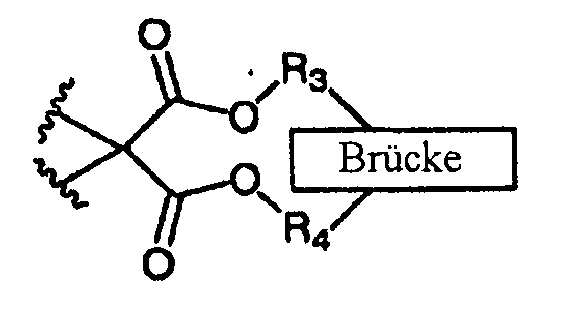
- methanofullerenes having one or more addends satisfying the formula:- in which R 3 and R 4 are independently selected from -[(CH 2 ) n O q ] p -R 5 in which n is preferably from 1 to 8 (most preferably 2), p is preferably 1 to 5 (most preferably 2 or 3), q is 0 or 1 and in which R 5 is preferably hydrogen, hydroxy, straight or branched alkyl (e.g. methyl or t-butyl), cycloalkyl (e.g. cyclohexyl), a heterocycle (e.g.
- an oxygen containing heterocycle such as tetrahydrofuranyl, tetrahydropyranyl), or a substituted or unsubstituted aromatic moiety (e.g. phenyl, naphthylen-yl, triphenylen-yl), said substituent(s) preferably being alkoxy).
- R 3 and R 4 may be linked via a bridging moiety, such as an ether moiety.
- a method for the formation of a patterned resist layer on a substrate surface by patternwise irradiation with actinic radiation comprising the steps of:-
- Step (i) may be achieved by application of the methanofullerene in solution, followed by removal of the solvent.
- Solvent may be removed by heating, a process which is commonly referred to as a soft pre-bake.
- Convenient coating techniques include spin coating (preferred) dipping and roller coating. Other conventional coating techniques include vacuum sublimation.
- spin coating it will be appreciated that the solids content of the coating solution can be adjusted to provide a desired film thickness based upon the specific spinning equipment utilized, and parameters such as the viscosity of the solution, the speed of the spinner and the amount of time allowed for spinning.
- the film thickness is not particularly limited and may be 10 nm or less to several hundred (e.g. 500) nanometers
- the substrate is not particularly limited, but in the preparation of electronic components, the substrate will normally be a silicon or silicon dioxide wafer for the production of microprocessors and other integrated circuit components.
- Aluminum-aluminum oxide, gallium arsenide and silicon nitride wafers can also serve as substrate.
- Solvents which may be used in step (i) include chloroform, chlorobenzene, dichlorobenzene, anisole, ethyl-3-ethoxy propionate and acetone.
- concentration of methanofullerene derivative is from about 1 to 10 mg/ml
- the solvent in step (i) is preferably anisole, ethyl-3-ethoxy propionate or acetone.
- Step (iii) is conveniently achieved by selectively dissolving the unirradiated areas of the coating layer in a second solvent (e.g. by immersion or spraying).
- Solvents which may be used in step (iii) include chloroform, chlorobenzene, dichlorobenzene, anisole, ethyl-3-ethoxy propionate, acetone, isopropyl alcohol:water.
- the solvent used in step (iii) is selected from anisole, 3-ethoxy propionate, isopropyl alcohol/water in a ratio of at least 1:1, preferably 7:3 and chlorobenzene/isopropyl alcohol, especially chlorobenzene/isopropyl alcohol in a ratio of 1:2 (increasing the ratio of isopropanol reduces the strength of the developer which in turn increases sensitivity at the cost of resolution.
- Step (ii) is preferably conducted using electron beam energy although excimer laser beams and X-rays may also be used.
- the patternwise irradiation may be achieved by scanning the actinic ray source according to the required pattern, or by using a mask formed to the pattern over the substrate.
- the method may include the additional step, between steps (ii) and (iii) of a post exposure bake, in which the substrate is heated to an elevated temperature (e.g. 50 to 150 °C, preferably about 100°C), for a predetermined period (e.g. 0.1 to 20 minutes, preferably about 1-2 minutes).
- an elevated temperature e.g. 50 to 150 °C, preferably about 100°C
- a predetermined period e.g. 0.1 to 20 minutes, preferably about 1-2 minutes.
- the methanofullerene is chemically amplified. That is, the coating layer formed in step (i) includes at least one additional component (sensitiser) which increases the sensitivity of the exposed layer to the actinic radiation of step (ii). It will be appreciated that when the coating layer is formed from solution, the additional component(s) are also in solution.
- the additional components are a photo acid generator and optionally a cross-linker.
- Suitable PAGs are described in US6,607,870 and include non-ionic, organic acid generators.
- Specific non-ionic organic acid generators include halogenated non-ionic compounds such as, for example, 1,1-bis[p-chlorophenyl]-2,2,2-trichloroethane (DDT); 1,1-bis[p-methoxyphenyl]-2,2,2-trichloroethane; 1,2,5,6,9,10-hexabromocyclododecane; 1,10-dibromodecane; 1,1-bis[p-chlorophenyl]2,2-dichloroethane; 4,4'-dichloro-2-(trichloromethyl)benzhydrol or 1,1-bis(chlorophenyl) 2-2,2-trichloroethanol; hexachlorodimethylsulfone; 2-chloro-6-(trichloromethyl)pyridine; 0,0-diethyl-O-(3,5,6-t
- Suitable photoacid generators are also disclosed in European Patent Application Nos. 0164248 and 0232972 . Especially preferred is triphenylsulphonium triflate. In addition to PAGs it is possible to use photoinitiators such as triarylsulfonium hexafluoroantiminate salts or triarylsulfonium hexafluorophosphate salts.
- Suitable amine-containing crosslinkers include urea-formaldehyde, melamine-formaldehyde, benzoguanamine-formaldehyde, glycoluril-formaldehyde resins and combinations thereof.
- Other suitable amine-based crosslinkers include the melamines manufactured by American Cyanamid Company such as Cymel(TM)300, 301, 303, 350, 370, 380, 1116 and 1130; benzoguanamine resins such as CymeI(TM)1123 and 1125; glycoluril resins CymeI(TM)1170, 1171, 1172; and urea-based resins BeetIe(TM)60, 65 and 80.
- polymeric amine-based resins may be prepared by the reaction of acrylamide or methacrylamide copolymers with formaldehyde in an alcohol-containing solution, or alternatively by the copolymerization of N-alkoxymethyl acrylamide or methacrylamide with other suitable monomers.
- epoxide crosslinkers may also be used, such as epoxy novolacs (e.g. DEN439 sold by Dow Chemicals).
- the melamines are preferred, and particularly preferred are hexaalkoxymethylmelamines such as the above identified CymeI(TM) resins, especially CymeI(TM) 300.
- a preferred mass ratio of methanofullerene to sensitiser is from about 1:0.1 to 1:1.
- a preferred ratio of methanofullerene by mass to cross linker by weight is from about 1:0.1 to 1:3.
- the developed substrate may be selectively processed on those substrate areas bared of the coating composition, for example by chemically etching or plating using procedures well known in the art.
- suitable etchants include a plasma gas etch and a hydrofluoric acid etching solution.
- the resist layer may be removed from the processed substrate using known stripping procedures.
- the historical background, types and processing of conventional photoresists are described by DeForest, Photoresist Materials and Processes, McGraw Hill Book Company, New York, ch.
- the invention further resides in a substrate treated in accordance with the process of the second aspect.
- reaction mixture was stirred for 24h and then filtered through a silica gel plug in a sintered glass filter funnel, eluting initially with toluene to remove excess C 60 and then eluting the products with CH 2 Cl 2 /MeOH (20/1).
- the second fraction was concentrated in vacuo yielding a dark brown solid, which was further purified by silica gel column chromatography (hexane/CH 2 Cl 2 , 1:1) to yield a mixture of ( MF02-01 ) as a brown solid (500mg, 69%).
- reaction mixture was stirred for 24h and then filtered through a silica gel plug in a sintered glass filter funnel, eluting initially with toluene to remove the excess C 60 and then eluting the products with CH 2 Cl 2 /MeOH (20/1).
- the second fraction was concentrated in vacuo yielding a dark brown solid, which was further purified by silica gel column chromatography (hexane/CH 2 Cl 2 , 1:1) to yielded a mixture of ( MF03-01 ) as a brown solid (78mg).
- reaction mixture was stirred for 24h and then filtered through a silica gel plug in a sintered glass filter funnel, eluting initially with toluene to remove excess C 60 and then eluting the products with CH 2 Cl 2 /MeOH (20/1).
- the second fraction was concentrated in vacuo yielding a dark brown solid, which was further purified by silica gel column chromatography (hexane/CH 2 Cl 2 , 1:1) to yield a mixture of ( MF03-04 ) as a brown solid (78mg).
- Example 1 Forming Films of a Fullerene Resist using a Safe Casting Solvent
- a solution of the multi-addend MF03-01 was prepared using the safe solvent anisole. 7.7 mg of the derivative was dissolved in 400 ⁇ l of the solvent. 50 ⁇ l of this solution was deposited on a square 4 cm 2 hydrogen terminated silicon substrate, which was then spun at 1000 RPM for 120 seconds, followed by 3000 RPM for 10 seconds. A smooth film with thickness 30 nm was created on the substrate.
- a further solution consisting of 2.7 mg of MF03-01, 0.85 mg of the crosslinker TMOM-BP (Honshu Chemicals) and 0.29 mg of the photoacid generator triphenylsulphonium triflate in 180 ⁇ l of anisole was used to prepare a chemically amplified film of fullerene derivative based resist on hydrogen terminated silicon (estimated thickness 50 nm), using the same conditions as mentioned above (with the exception that the first spin speed was held for 60 seconds instead of 120).
- the compound MF02-01 has been successfully spin coated from both anisole and ethyl-3-ethoxy propionate, which is also considered to be a safe solvent. So far it has been found that anisole or ethyl-3-ethoxy propionate can be substituted for the previously used chloroform for methanofullerenes used with or without chemical amplification. Preliminary data suggests that acetone can also be used.
- Example 2 Developing Films of a Fullerene Resist using a Safe Developer
- MF02-01 is a multiple addend derivative of C 60 prepared as a mixture of tetra, penta and hexa addend derivatives. Various different ratios of the three different adducts have been prepared. MF02-01A is mainly hexa-adduct whilst MF02-01D is approximately an equal mixture of the three derivatives. In terms of resist formation, the results for MFO2-01A and MF02-01D are similar, with only minor differences in the exact sensitivities. Results for MF02-01D are presented below.
- Films of pure MF02-01D and MF02-01D[CA] were prepared.
- the chemically amplified film incorporated PAG03-01 and CL03-01 in a ratio of 1mg MF02-01D: 0.28 mg PAG03-01: 3.125 ⁇ l CL03-01.
- a solution of this mixture, with a concentration of 10.6 mg/ml of MF02-01D in chloroform was prepared.
- Films were formed on hydrogen terminated silicon substrate by spin coating as described above (thickness 100nm). Shown in figure 2 is a graph of the response to irradiation of several different films of the chemically amplified and non amplified films for two different developers (monochlorobenzene and monochlorobenzene/isopropanol 1:2).
- MF03-01 is a multiple addend derivative of C 60 , somewhat smaller than MF02-01.
- the compound is again prepared as a mixture of tetra, penta and hexa adduct derivatives. In this case only one ratio of derivatives was investigated.
- the sensitivity of pure MF03-01 was found to be ⁇ 360 ⁇ C/cm 2 , using MCB as the developer.
- a wide range of derivative, photoacid generator and crosslinker ratios was then investigated. The best results were seen for a film with the proportions 1 mg MF03-01: 0.224 mg PAG03-01: 1.04 ⁇ l CL03-01.
- a film made with this mixture, exposed to electrons, and treated with a PEB of 100 °C for 60 seconds, before development with MCB was found to have a sensitivity of ⁇ 12 ⁇ C/cm 2 .
- the response curve for this film is shown in figure 3 .
- Example 5 Response to Electron Irradiation of MF03-04 and MF03-04[CA]
- MF03-04 is a multiple addend derivative of C 60 prepared as a mixture of tetra, penta and hexa addend derivatives.
- FIG. 5 Shown in figure 5 is a graph of the response to irradiation of a film of the chemically amplified and a non amplified film. It can be seen from figure 5 at the incorporation of the chemical amplification components substantially improves the sensitivity of the resist from about 650 ⁇ C/cm 2 to about 7.5 ⁇ C/cm 2 . The steepness of the response curves is similar, indicating that the contrast of the amplified resist material is comparable to that of the unamplified resist.
- Example 6 Response to Electron Irradiation of MF03-04[CA*] prepared using a different photoinitiator and crosslinkers to Example 6
- MF03-04 is a multiple addend derivative of C 60 prepared as a mixture of tetra, penta and hexa addend derivatives
- Films of pure MF03-04 and MF03-04[CA*] were prepared (thickness 100 nm in both cases).
- the chemically amplified film incorporated the photoinitiator (PI) Triarylsulfonium hexafluroantimonate salts (Dow) and the crosslinker (CL) DEN438 (Dow) in a ratio of 1mg MF03-04: 1 mg PI: 2 mg CL.
- Films were formed on hydrogen terminate silicon substrate by spin coating as described above. Shown in figure 6 is a graph of the response to irradiation of a film of the chemically amplified film (see figure 6 for a non amplified film).
- ECR Electron Cyclotron Resonance
- RF Power 20W
- DC Self Bias 110V
- Microwave Power 250W
- Etching Gas SF 6
- Etching Gas Flow Rate 5 sccm
- Chamber Pressure 0.001 Torr
- Etch Time 20 minutes.
- etch durability a square pattern of 100 microns on a side was defined in each of the resist films and the thickness of the film was measured with a surface profiler (height 1). The sample was then etched, and the height of the feature was again measured (height 2). Finally any remaining film was removed using plasma ashing as described above and the height was once again measured (height 3).
- the etch durability of the material in terms of the etch durability of the silicon substrate is then given by: hight 3
- fullerene derivatives are high resolution, high durability electron beam resists, but they suffer from unsafe processing solvents and low sensitivity.
- the inventors have expanded the range of useful fullerene resist materials and have demonstrated that by the process of chemical amplification it is possible to substantially increase the sensitivity of fullerene derivative resists (both those already known and those newly proposed), by one to two orders of magnitude, into the industrially useful sub-10 ⁇ C/cm 2 region. It has also been shown that several safe solvents exist for both the casting and the developing processes. It has also been shown that the etch ratio of the chemical amplified formulations is not substantially reduced over that of the pure derivatives. Finally, it has been demonstrated that the resists can be easily removed by oxygen plasma ashing.
Landscapes
- Physics & Mathematics (AREA)
- Chemical & Material Sciences (AREA)
- Engineering & Computer Science (AREA)
- Nanotechnology (AREA)
- Spectroscopy & Molecular Physics (AREA)
- General Physics & Mathematics (AREA)
- Condensed Matter Physics & Semiconductors (AREA)
- Crystallography & Structural Chemistry (AREA)
- Materials Engineering (AREA)
- Composite Materials (AREA)
- Materials For Photolithography (AREA)
- Organic Low-Molecular-Weight Compounds And Preparation Thereof (AREA)
- Macromolecular Compounds Obtained By Forming Nitrogen-Containing Linkages In General (AREA)
- Exposure Of Semiconductors, Excluding Electron Or Ion Beam Exposure (AREA)
- Photosensitive Polymer And Photoresist Processing (AREA)
- Exposure And Positioning Against Photoresist Photosensitive Materials (AREA)
Claims (15)
- Verwendung eines Methanfulleren-Derivats mit mehreren offenendigen Liganden, wobei Methanfulleren durch die Formel C2xCR1R2)m dargestellt wird, wobei x mindestens gleich 10 ist, m mindestens gleich 2 ist, wobei jeder durch CR1R2 dargestellte Ligand gleich oder unterschiedlich ist, und wobei jedes R1 und R2 eine einwertige organische Gruppe oder eine zweiwertige organische Gruppe ist, die eine Ringstruktur bildet, indem sie an die Fulleren-Schale gebunden wird, oder falls sowohl R1 als auch R2 eines Liganden zweiwertige Gruppen sind, diese aneinander gebunden sein können um eine Ringstruktur zu bilden, mit der Ausnahme, daß mindestens zwei R1 oder zwei R2 einwertig sind, oder eines Gemischs derartiger Derivate als Resistmaterial.
- Verwendung nach Anspruch 1, wobei das Resistmaterial ein Gemisch von Derivaten aufweist, wobei sich die Derivate nur in dem Wert von m unterscheiden.
- Verwendung nach Anspruch 1 oder 2, wobei R1 und R2 für jeden Liganden gleich sind.
- Verwendung nach einem der vorstehenden Ansprüche, wobei mindestens eine der Gruppen R1 und R2 eine Polymerkomponente enthält.
- Verwendung nach einem der vorstehenden Ansprüche, wobei das Methanfulleren-Derivat einen oder mehrere Liganden aufweist, die der folgenden Formel genügen:

- Verwendung nach einem der vorstehenden Ansprüche, wobei das Methanfulleren-Derivat einen oder mehrere Liganden aufweist, die der folgenden Formel genügen:
- Verwendung nach einem der Ansprüche 5 oder 6, wobei das Methanfulleren-Derivat einen oder mehrere der folgenden Liganden aufweist:


- Verfahren zur Bildung einer strukturierten Resistschicht auf einer Substratoberfläche durch strukturierte Bestrahlung mit aktinischer Strahlung, mit den folgenden Schritten:(i) Ausbilden einer Überzugsschicht, die ein Methanfulleren nach einem der vorstehenden Ansprüche aufweist, auf der Substratoberfläche,(ii) strukturierte Bestrahlung der Überzugsschicht, und(iii) Entfernen unbestrahlter Bereiche der Überzugsschicht.
- Verfahren nach Anspruch 8, wobei der Schritt (i) durch Auftragen des Methanfullerens in Lösung und anschließendes Entfernen des Lösungsmittels ausgeführt wird, wobei das Lösungsmittel unter Chloroform, Chlorbenzol, Dichlorbenzol, Anisol, Ethyl-3-ethoxypropionat und Aceton ausgewählt ist.
- Verfahren nach Anspruch 8 oder 9, wobei der Schritt (iii) durch selektives Auflösen, der unbestrahlten Bereiche der Überzugsschicht in einem zweiten Lösungsmittel ausgeführt wird, wobei das zweite Lösungsmittel unter Chloroform, Chlorbenzol, Dichlorbenzol, Anisol, Ethyl-3-ethoxypropionat, Aceton, Isopropylalkohol/Wasser und Chlorbenzol/Isopropylalkohol ausgewählt ist.
- Verfahren nach Anspruch 10, wobei das im Schritt (iii) verwendete Lösungsmittel unter Anisol, 3-Ethyoxypropionat, Isopropylalkohol/Wasser in einem Verhältnis von mindestens 1:1 und Chlorbenzol/Isopropylalkohol in einem Verhältnis von 1:2 ausgewählt ist.
- Verfahren nach einem der Ansprüche 8 bis 11, wobei das Methanfulleren chemisch verstärkt wird, indem in die im Schritt (i) gebildete Überzugsschicht mindestens eine zusätzliche Komponente eingebracht wird, welche die Empfindlichkeit der bestrahlten Schicht gegen die aktinische Strahlung im Schritt (ii) erhöht.
- Verfahren nach Anspruch 12, wobei die zusätzlichen Komponenten ein Photosäuregenerator und ein Vernetzungsmittel sind.
- Verfahren nach Anspruch 13, wobei der Photosäuregenerator Triphenylsulfoniumtriflat und das Vernetzungsmittel ein Hexaalkoxymethylamin ist.
- Substrat, das mit dem Verfahren nach einem der Ansprüche 8 bis 14 behandelt wird.
Applications Claiming Priority (2)
| Application Number | Priority Date | Filing Date | Title |
|---|---|---|---|
| GB0420702A GB0420702D0 (en) | 2004-09-17 | 2004-09-17 | Use of methanofullerene derivatives as resist materials and method for forming a resist layer |
| PCT/GB2005/003587 WO2006030234A2 (en) | 2004-09-17 | 2005-09-19 | Use of methanofullerene derivatives as resist materials and method for forming a resist layer |
Publications (2)
| Publication Number | Publication Date |
|---|---|
| EP1789849A2 EP1789849A2 (de) | 2007-05-30 |
| EP1789849B1 true EP1789849B1 (de) | 2009-05-06 |
Family
ID=33306753
Family Applications (1)
| Application Number | Title | Priority Date | Filing Date |
|---|---|---|---|
| EP05783725A Expired - Lifetime EP1789849B1 (de) | 2004-09-17 | 2005-09-19 | Verwendung von methanofullerenderivaten als resistmaterialien und verfahren zur bildung einer resistschicht |
Country Status (7)
| Country | Link |
|---|---|
| US (1) | US8034546B2 (de) |
| EP (1) | EP1789849B1 (de) |
| JP (1) | JP4980912B2 (de) |
| AT (1) | ATE430952T1 (de) |
| DE (1) | DE602005014369D1 (de) |
| GB (1) | GB0420702D0 (de) |
| WO (1) | WO2006030234A2 (de) |
Families Citing this family (19)
| Publication number | Priority date | Publication date | Assignee | Title |
|---|---|---|---|---|
| EP2087404A4 (de) * | 2006-11-20 | 2010-12-29 | Jsr Corp | Zusammensetzung zur resistunterschichtfilmbildung und verfahren zur strukturbildung |
| TWI366565B (en) * | 2007-06-06 | 2012-06-21 | Otsuka Pharma Co Ltd | Quinolone compound and pharmaceutical composition |
| GB0913919D0 (en) | 2009-08-10 | 2009-09-16 | Univ Birmingham | Method of forming an electrical circuit using fullerene derivatives |
| GB0920231D0 (en) | 2009-11-18 | 2010-01-06 | Univ Birmingham | Photoresist composition |
| JP5068831B2 (ja) * | 2010-02-05 | 2012-11-07 | 信越化学工業株式会社 | レジスト下層膜材料、レジスト下層膜形成方法、パターン形成方法 |
| JP5757286B2 (ja) * | 2010-03-01 | 2015-07-29 | 日産化学工業株式会社 | フラーレン誘導体を含むレジスト下層膜形成組成物 |
| KR101783729B1 (ko) * | 2010-09-16 | 2017-10-10 | 후지필름 가부시키가이샤 | 패턴 형성 방법, 화학증폭형 레지스트 조성물, 및 레지스트 막 |
| US20150010703A1 (en) * | 2012-02-10 | 2015-01-08 | The University Of Birmingham | Spin on Hard-Mask Material |
| JP5935651B2 (ja) * | 2012-10-18 | 2016-06-15 | 三菱商事株式会社 | 極紫外線光及び電子ビーム露光用レジスト組成物、並びにこれを用いたレジストパターン形成方法 |
| US9256126B2 (en) | 2012-11-14 | 2016-02-09 | Irresistible Materials Ltd | Methanofullerenes |
| US9220432B2 (en) * | 2013-03-02 | 2015-12-29 | C. R. Bard, Inc. | Method and system of utilizing ECG signal for central venous catheter tip positioning |
| US9323149B2 (en) * | 2013-03-05 | 2016-04-26 | Irresistible Materials Ltd | Methanofullerenes |
| WO2014190070A1 (en) * | 2013-05-22 | 2014-11-27 | Robinson Alex Philip Graaham | Fullerenes |
| EP3063592B1 (de) | 2013-10-30 | 2021-04-07 | California Institute of Technology | Direkte fotostrukturierung von robusten und unterschiedlichen materialien |
| US9229322B2 (en) * | 2013-10-31 | 2016-01-05 | Alex Phillip Graham Robinson | Composition of matter and molecular resist made therefrom |
| US10095112B2 (en) * | 2017-02-24 | 2018-10-09 | Irresistible Materials Ltd | Multiple trigger photoresist compositions and methods |
| KR20240040748A (ko) * | 2021-07-04 | 2024-03-28 | 알렉스 필립 그레이엄 로빈손 | 강화된 euv 포토레지스트 및 그 사용 방법 |
| US20250138420A1 (en) * | 2022-05-22 | 2025-05-01 | Irresistible Materials Ltd | Enhanced euv photoresists and methods of their use |
| KR20250113985A (ko) * | 2022-07-07 | 2025-07-28 | 알렉스 필립 그레이엄 로빈손 | 강화된 euv 물질, 포토레지스트 및 이의 사용 방법 |
Family Cites Families (9)
| Publication number | Priority date | Publication date | Assignee | Title |
|---|---|---|---|---|
| JP2814165B2 (ja) * | 1992-06-30 | 1998-10-22 | 日本石油株式会社 | 感光材料 |
| JP2860399B2 (ja) | 1996-01-31 | 1999-02-24 | 工業技術院長 | パターン形成方法 |
| JP3032833B2 (ja) * | 1997-09-22 | 2000-04-17 | ザ ユニバーシティ オブ バーミンガム | 電子線レジスト |
| JP3521710B2 (ja) | 1997-09-30 | 2004-04-19 | Jsr株式会社 | 感放射線性樹脂組成物 |
| JP3026188B2 (ja) | 1998-03-11 | 2000-03-27 | 工業技術院長 | 電子線レジスト、レジストパターンの形成方法及び微細パターンの形成方法 |
| US6800416B2 (en) * | 2002-01-09 | 2004-10-05 | Clariant Finance (Bvi) Ltd. | Negative deep ultraviolet photoresist |
| JP2005053832A (ja) * | 2003-08-04 | 2005-03-03 | Nippon Telegr & Teleph Corp <Ntt> | フラーレン誘導体およびフラーレン複合化レジスト |
| JP2005266798A (ja) * | 2004-02-19 | 2005-09-29 | Tokyo Ohka Kogyo Co Ltd | フォトレジスト組成物およびレジストパターン形成方法 |
| US20070190447A1 (en) * | 2004-02-19 | 2007-08-16 | Tokyo Ohkakogyo Co. Ltd. | Photoresist composition and method of forming resist pattern |
-
2004
- 2004-09-17 GB GB0420702A patent/GB0420702D0/en not_active Ceased
-
2005
- 2005-09-19 JP JP2007531833A patent/JP4980912B2/ja not_active Expired - Fee Related
- 2005-09-19 WO PCT/GB2005/003587 patent/WO2006030234A2/en not_active Ceased
- 2005-09-19 DE DE602005014369T patent/DE602005014369D1/de not_active Expired - Lifetime
- 2005-09-19 AT AT05783725T patent/ATE430952T1/de not_active IP Right Cessation
- 2005-09-19 EP EP05783725A patent/EP1789849B1/de not_active Expired - Lifetime
- 2005-09-19 US US11/662,904 patent/US8034546B2/en not_active Expired - Fee Related
Also Published As
| Publication number | Publication date |
|---|---|
| GB0420702D0 (en) | 2004-10-20 |
| WO2006030234A3 (en) | 2006-09-14 |
| EP1789849A2 (de) | 2007-05-30 |
| JP2008513820A (ja) | 2008-05-01 |
| ATE430952T1 (de) | 2009-05-15 |
| US20080118874A1 (en) | 2008-05-22 |
| DE602005014369D1 (de) | 2009-06-18 |
| JP4980912B2 (ja) | 2012-07-18 |
| US8034546B2 (en) | 2011-10-11 |
| WO2006030234A2 (en) | 2006-03-23 |
Similar Documents
| Publication | Publication Date | Title |
|---|---|---|
| US8034546B2 (en) | Use of methanofullerne derivatives as resist materials and method for forming a resist layer | |
| EP0811879B1 (de) | Entwickeltes Resistmaterial und sein Herstellungsverfahren | |
| US6753129B2 (en) | Method and apparatus for modification of chemically amplified photoresist by electron beam exposure | |
| JP3859353B2 (ja) | ネガ型レジスト組成物およびレジストパターンの形成方法 | |
| US20080032243A1 (en) | Photoresist Coating Composition and Method for Forming Fine Contact of Semiconductor Device | |
| JPS6363892B2 (de) | ||
| TW200403529A (en) | Resist composition suitable for short wavelength exposure and resist pattern forming method | |
| EP1238314A1 (de) | Modifikation von bei 193 nm empfindlichen photoresistmaterialien durch elektronenstrahlbelichtung | |
| EP0492256B1 (de) | Photolithographische Strukturerzeugung | |
| JP2013511502A (ja) | フォトレジスト組成物 | |
| JP3026188B2 (ja) | 電子線レジスト、レジストパターンの形成方法及び微細パターンの形成方法 | |
| US5776657A (en) | Wet-chemical developable, etch-stable photoresist for UV radiation with a wavelength below 200 NM | |
| US6451501B1 (en) | Acid sensitive copolymer, resist composition and resist pattern forming method | |
| JP3824288B2 (ja) | ポジ型感光性樹脂組成物 | |
| JPS5949536A (ja) | 微細パタ−ン形成方法 | |
| JP3607432B2 (ja) | 感光性組成物 | |
| US7670749B2 (en) | Resist material and method for forming a patterned resist layer on a substrate | |
| JP3249194B2 (ja) | 感光性レジスト組成物 | |
| US6989227B2 (en) | E-beam curable resist and process for e-beam curing the resist | |
| WO2006030240A2 (en) | Novel resist material | |
| US20020015917A1 (en) | Multi-oxygen containing compound for preventing acid diffusion, and photoresist composition containing the same | |
| JPH04212160A (ja) | 感光性樹脂組成物 | |
| JPH06194848A (ja) | 電子部品のパターン形成方法 | |
| JPH0980753A (ja) | 感光性組成物 | |
| JPH01241544A (ja) | 感光性組成物 |
Legal Events
| Date | Code | Title | Description |
|---|---|---|---|
| PUAI | Public reference made under article 153(3) epc to a published international application that has entered the european phase |
Free format text: ORIGINAL CODE: 0009012 |
|
| 17P | Request for examination filed |
Effective date: 20070313 |
|
| AK | Designated contracting states |
Kind code of ref document: A2 Designated state(s): AT BE BG CH CY CZ DE DK EE ES FI FR GB GR HU IE IS IT LI LT LU LV MC NL PL PT RO SE SI SK TR |
|
| DAX | Request for extension of the european patent (deleted) | ||
| 17Q | First examination report despatched |
Effective date: 20080102 |
|
| GRAP | Despatch of communication of intention to grant a patent |
Free format text: ORIGINAL CODE: EPIDOSNIGR1 |
|
| GRAS | Grant fee paid |
Free format text: ORIGINAL CODE: EPIDOSNIGR3 |
|
| GRAA | (expected) grant |
Free format text: ORIGINAL CODE: 0009210 |
|
| AK | Designated contracting states |
Kind code of ref document: B1 Designated state(s): AT BE BG CH CY CZ DE DK EE ES FI FR GB GR HU IE IS IT LI LT LU LV MC NL PL PT RO SE SI SK TR |
|
| REG | Reference to a national code |
Ref country code: GB Ref legal event code: FG4D |
|
| REG | Reference to a national code |
Ref country code: CH Ref legal event code: EP |
|
| REG | Reference to a national code |
Ref country code: IE Ref legal event code: FG4D |
|
| REF | Corresponds to: |
Ref document number: 602005014369 Country of ref document: DE Date of ref document: 20090618 Kind code of ref document: P |
|
| PG25 | Lapsed in a contracting state [announced via postgrant information from national office to epo] |
Ref country code: LT Free format text: LAPSE BECAUSE OF FAILURE TO SUBMIT A TRANSLATION OF THE DESCRIPTION OR TO PAY THE FEE WITHIN THE PRESCRIBED TIME-LIMIT Effective date: 20090506 Ref country code: PT Free format text: LAPSE BECAUSE OF FAILURE TO SUBMIT A TRANSLATION OF THE DESCRIPTION OR TO PAY THE FEE WITHIN THE PRESCRIBED TIME-LIMIT Effective date: 20090906 Ref country code: ES Free format text: LAPSE BECAUSE OF FAILURE TO SUBMIT A TRANSLATION OF THE DESCRIPTION OR TO PAY THE FEE WITHIN THE PRESCRIBED TIME-LIMIT Effective date: 20090817 Ref country code: FI Free format text: LAPSE BECAUSE OF FAILURE TO SUBMIT A TRANSLATION OF THE DESCRIPTION OR TO PAY THE FEE WITHIN THE PRESCRIBED TIME-LIMIT Effective date: 20090506 Ref country code: AT Free format text: LAPSE BECAUSE OF FAILURE TO SUBMIT A TRANSLATION OF THE DESCRIPTION OR TO PAY THE FEE WITHIN THE PRESCRIBED TIME-LIMIT Effective date: 20090506 |
|
| PG25 | Lapsed in a contracting state [announced via postgrant information from national office to epo] |
Ref country code: LV Free format text: LAPSE BECAUSE OF FAILURE TO SUBMIT A TRANSLATION OF THE DESCRIPTION OR TO PAY THE FEE WITHIN THE PRESCRIBED TIME-LIMIT Effective date: 20090506 Ref country code: PL Free format text: LAPSE BECAUSE OF FAILURE TO SUBMIT A TRANSLATION OF THE DESCRIPTION OR TO PAY THE FEE WITHIN THE PRESCRIBED TIME-LIMIT Effective date: 20090506 Ref country code: IS Free format text: LAPSE BECAUSE OF FAILURE TO SUBMIT A TRANSLATION OF THE DESCRIPTION OR TO PAY THE FEE WITHIN THE PRESCRIBED TIME-LIMIT Effective date: 20090906 Ref country code: SE Free format text: LAPSE BECAUSE OF FAILURE TO SUBMIT A TRANSLATION OF THE DESCRIPTION OR TO PAY THE FEE WITHIN THE PRESCRIBED TIME-LIMIT Effective date: 20090806 Ref country code: SI Free format text: LAPSE BECAUSE OF FAILURE TO SUBMIT A TRANSLATION OF THE DESCRIPTION OR TO PAY THE FEE WITHIN THE PRESCRIBED TIME-LIMIT Effective date: 20090506 |
|
| PG25 | Lapsed in a contracting state [announced via postgrant information from national office to epo] |
Ref country code: RO Free format text: LAPSE BECAUSE OF FAILURE TO SUBMIT A TRANSLATION OF THE DESCRIPTION OR TO PAY THE FEE WITHIN THE PRESCRIBED TIME-LIMIT Effective date: 20090506 Ref country code: CZ Free format text: LAPSE BECAUSE OF FAILURE TO SUBMIT A TRANSLATION OF THE DESCRIPTION OR TO PAY THE FEE WITHIN THE PRESCRIBED TIME-LIMIT Effective date: 20090506 Ref country code: EE Free format text: LAPSE BECAUSE OF FAILURE TO SUBMIT A TRANSLATION OF THE DESCRIPTION OR TO PAY THE FEE WITHIN THE PRESCRIBED TIME-LIMIT Effective date: 20090506 Ref country code: DK Free format text: LAPSE BECAUSE OF FAILURE TO SUBMIT A TRANSLATION OF THE DESCRIPTION OR TO PAY THE FEE WITHIN THE PRESCRIBED TIME-LIMIT Effective date: 20090506 |
|
| PG25 | Lapsed in a contracting state [announced via postgrant information from national office to epo] |
Ref country code: BE Free format text: LAPSE BECAUSE OF FAILURE TO SUBMIT A TRANSLATION OF THE DESCRIPTION OR TO PAY THE FEE WITHIN THE PRESCRIBED TIME-LIMIT Effective date: 20090506 Ref country code: SK Free format text: LAPSE BECAUSE OF FAILURE TO SUBMIT A TRANSLATION OF THE DESCRIPTION OR TO PAY THE FEE WITHIN THE PRESCRIBED TIME-LIMIT Effective date: 20090506 |
|
| PLBE | No opposition filed within time limit |
Free format text: ORIGINAL CODE: 0009261 |
|
| STAA | Information on the status of an ep patent application or granted ep patent |
Free format text: STATUS: NO OPPOSITION FILED WITHIN TIME LIMIT |
|
| PG25 | Lapsed in a contracting state [announced via postgrant information from national office to epo] |
Ref country code: BG Free format text: LAPSE BECAUSE OF FAILURE TO SUBMIT A TRANSLATION OF THE DESCRIPTION OR TO PAY THE FEE WITHIN THE PRESCRIBED TIME-LIMIT Effective date: 20090806 |
|
| 26N | No opposition filed |
Effective date: 20100209 |
|
| PG25 | Lapsed in a contracting state [announced via postgrant information from national office to epo] |
Ref country code: MC Free format text: LAPSE BECAUSE OF NON-PAYMENT OF DUE FEES Effective date: 20090930 |
|
| REG | Reference to a national code |
Ref country code: CH Ref legal event code: PL |
|
| PG25 | Lapsed in a contracting state [announced via postgrant information from national office to epo] |
Ref country code: CH Free format text: LAPSE BECAUSE OF NON-PAYMENT OF DUE FEES Effective date: 20090930 Ref country code: GR Free format text: LAPSE BECAUSE OF FAILURE TO SUBMIT A TRANSLATION OF THE DESCRIPTION OR TO PAY THE FEE WITHIN THE PRESCRIBED TIME-LIMIT Effective date: 20090807 Ref country code: LI Free format text: LAPSE BECAUSE OF NON-PAYMENT OF DUE FEES Effective date: 20090930 |
|
| PG25 | Lapsed in a contracting state [announced via postgrant information from national office to epo] |
Ref country code: LU Free format text: LAPSE BECAUSE OF NON-PAYMENT OF DUE FEES Effective date: 20090919 |
|
| PG25 | Lapsed in a contracting state [announced via postgrant information from national office to epo] |
Ref country code: HU Free format text: LAPSE BECAUSE OF FAILURE TO SUBMIT A TRANSLATION OF THE DESCRIPTION OR TO PAY THE FEE WITHIN THE PRESCRIBED TIME-LIMIT Effective date: 20091107 |
|
| PG25 | Lapsed in a contracting state [announced via postgrant information from national office to epo] |
Ref country code: TR Free format text: LAPSE BECAUSE OF FAILURE TO SUBMIT A TRANSLATION OF THE DESCRIPTION OR TO PAY THE FEE WITHIN THE PRESCRIBED TIME-LIMIT Effective date: 20090506 |
|
| PG25 | Lapsed in a contracting state [announced via postgrant information from national office to epo] |
Ref country code: CY Free format text: LAPSE BECAUSE OF FAILURE TO SUBMIT A TRANSLATION OF THE DESCRIPTION OR TO PAY THE FEE WITHIN THE PRESCRIBED TIME-LIMIT Effective date: 20090506 |
|
| PGFP | Annual fee paid to national office [announced via postgrant information from national office to epo] |
Ref country code: NL Payment date: 20140919 Year of fee payment: 10 |
|
| PGFP | Annual fee paid to national office [announced via postgrant information from national office to epo] |
Ref country code: IT Payment date: 20140924 Year of fee payment: 10 |
|
| REG | Reference to a national code |
Ref country code: FR Ref legal event code: PLFP Year of fee payment: 11 |
|
| PGFP | Annual fee paid to national office [announced via postgrant information from national office to epo] |
Ref country code: IE Payment date: 20150907 Year of fee payment: 11 |
|
| PGFP | Annual fee paid to national office [announced via postgrant information from national office to epo] |
Ref country code: FR Payment date: 20150923 Year of fee payment: 11 |
|
| PG25 | Lapsed in a contracting state [announced via postgrant information from national office to epo] |
Ref country code: IT Free format text: LAPSE BECAUSE OF NON-PAYMENT OF DUE FEES Effective date: 20150919 |
|
| REG | Reference to a national code |
Ref country code: NL Ref legal event code: MM Effective date: 20151001 |
|
| PG25 | Lapsed in a contracting state [announced via postgrant information from national office to epo] |
Ref country code: NL Free format text: LAPSE BECAUSE OF NON-PAYMENT OF DUE FEES Effective date: 20151001 |
|
| PGFP | Annual fee paid to national office [announced via postgrant information from national office to epo] |
Ref country code: GB Payment date: 20160926 Year of fee payment: 12 |
|
| PGFP | Annual fee paid to national office [announced via postgrant information from national office to epo] |
Ref country code: DE Payment date: 20160928 Year of fee payment: 12 |
|
| REG | Reference to a national code |
Ref country code: IE Ref legal event code: MM4A |
|
| REG | Reference to a national code |
Ref country code: FR Ref legal event code: ST Effective date: 20170531 |
|
| PG25 | Lapsed in a contracting state [announced via postgrant information from national office to epo] |
Ref country code: FR Free format text: LAPSE BECAUSE OF NON-PAYMENT OF DUE FEES Effective date: 20160930 Ref country code: IE Free format text: LAPSE BECAUSE OF NON-PAYMENT OF DUE FEES Effective date: 20160919 |
|
| REG | Reference to a national code |
Ref country code: DE Ref legal event code: R119 Ref document number: 602005014369 Country of ref document: DE |
|
| GBPC | Gb: european patent ceased through non-payment of renewal fee |
Effective date: 20170919 |
|
| PG25 | Lapsed in a contracting state [announced via postgrant information from national office to epo] |
Ref country code: GB Free format text: LAPSE BECAUSE OF NON-PAYMENT OF DUE FEES Effective date: 20170919 Ref country code: DE Free format text: LAPSE BECAUSE OF NON-PAYMENT OF DUE FEES Effective date: 20180404 |