EP1801823B1 - Element multicouche et son procédé de fabrication - Google Patents
Element multicouche et son procédé de fabrication Download PDFInfo
- Publication number
- EP1801823B1 EP1801823B1 EP06026321.7A EP06026321A EP1801823B1 EP 1801823 B1 EP1801823 B1 EP 1801823B1 EP 06026321 A EP06026321 A EP 06026321A EP 1801823 B1 EP1801823 B1 EP 1801823B1
- Authority
- EP
- European Patent Office
- Prior art keywords
- dielectric
- ppm
- concentration
- film
- layer
- Prior art date
- Legal status (The legal status is an assumption and is not a legal conclusion. Google has not performed a legal analysis and makes no representation as to the accuracy of the status listed.)
- Ceased
Links
Images



Classifications
-
- H—ELECTRICITY
- H01—ELECTRIC ELEMENTS
- H01G—CAPACITORS; CAPACITORS, RECTIFIERS, DETECTORS, SWITCHING DEVICES, LIGHT-SENSITIVE OR TEMPERATURE-SENSITIVE DEVICES OF THE ELECTROLYTIC TYPE
- H01G2/00—Details of capacitors not covered by a single one of groups H01G4/00-H01G11/00
- H01G2/02—Mountings
- H01G2/06—Mountings specially adapted for mounting on a printed-circuit support
-
- H—ELECTRICITY
- H01—ELECTRIC ELEMENTS
- H01G—CAPACITORS; CAPACITORS, RECTIFIERS, DETECTORS, SWITCHING DEVICES, LIGHT-SENSITIVE OR TEMPERATURE-SENSITIVE DEVICES OF THE ELECTROLYTIC TYPE
- H01G4/00—Fixed capacitors; Processes of their manufacture
- H01G4/33—Thin- or thick-film capacitors (thin- or thick-film circuits; capacitors without a potential-jump or surface barrier specially adapted for integrated circuits, details thereof, multistep manufacturing processes therefor)
-
- H—ELECTRICITY
- H01—ELECTRIC ELEMENTS
- H01G—CAPACITORS; CAPACITORS, RECTIFIERS, DETECTORS, SWITCHING DEVICES, LIGHT-SENSITIVE OR TEMPERATURE-SENSITIVE DEVICES OF THE ELECTROLYTIC TYPE
- H01G4/00—Fixed capacitors; Processes of their manufacture
- H01G4/002—Details
- H01G4/005—Electrodes
- H01G4/008—Selection of materials
-
- H—ELECTRICITY
- H01—ELECTRIC ELEMENTS
- H01G—CAPACITORS; CAPACITORS, RECTIFIERS, DETECTORS, SWITCHING DEVICES, LIGHT-SENSITIVE OR TEMPERATURE-SENSITIVE DEVICES OF THE ELECTROLYTIC TYPE
- H01G4/00—Fixed capacitors; Processes of their manufacture
- H01G4/002—Details
- H01G4/018—Dielectrics
- H01G4/06—Solid dielectrics
- H01G4/14—Organic dielectrics
- H01G4/18—Organic dielectrics of synthetic material, e.g. derivatives of cellulose
-
- H—ELECTRICITY
- H05—ELECTRIC TECHNIQUES NOT OTHERWISE PROVIDED FOR
- H05K—PRINTED CIRCUITS; CASINGS OR CONSTRUCTIONAL DETAILS OF ELECTRIC APPARATUS; MANUFACTURE OF ASSEMBLAGES OF ELECTRICAL COMPONENTS
- H05K1/00—Printed circuits
- H05K1/16—Printed circuits incorporating printed electric components, e.g. printed resistors, capacitors or inductors
- H05K1/162—Printed circuits incorporating printed electric components, e.g. printed resistors, capacitors or inductors incorporating printed capacitors
-
- H—ELECTRICITY
- H05—ELECTRIC TECHNIQUES NOT OTHERWISE PROVIDED FOR
- H05K—PRINTED CIRCUITS; CASINGS OR CONSTRUCTIONAL DETAILS OF ELECTRIC APPARATUS; MANUFACTURE OF ASSEMBLAGES OF ELECTRICAL COMPONENTS
- H05K3/00—Apparatus or processes for manufacturing printed circuits
- H05K3/38—Improvement of the adhesion between the insulating substrate and the metal
-
- H—ELECTRICITY
- H10—SEMICONDUCTOR DEVICES; ELECTRIC SOLID-STATE DEVICES NOT OTHERWISE PROVIDED FOR
- H10D—INORGANIC ELECTRIC SEMICONDUCTOR DEVICES
- H10D86/00—Integrated devices formed in or on insulating or conducting substrates, e.g. formed in silicon-on-insulator [SOI] substrates or on stainless steel or glass substrates
- H10D86/80—Integrated devices formed in or on insulating or conducting substrates, e.g. formed in silicon-on-insulator [SOI] substrates or on stainless steel or glass substrates characterised by multiple passive components, e.g. resistors, capacitors or inductors
- H10D86/85—Integrated devices formed in or on insulating or conducting substrates, e.g. formed in silicon-on-insulator [SOI] substrates or on stainless steel or glass substrates characterised by multiple passive components, e.g. resistors, capacitors or inductors characterised by only passive components
-
- H—ELECTRICITY
- H05—ELECTRIC TECHNIQUES NOT OTHERWISE PROVIDED FOR
- H05K—PRINTED CIRCUITS; CASINGS OR CONSTRUCTIONAL DETAILS OF ELECTRIC APPARATUS; MANUFACTURE OF ASSEMBLAGES OF ELECTRICAL COMPONENTS
- H05K2201/00—Indexing scheme relating to printed circuits covered by H05K1/00
- H05K2201/01—Dielectrics
- H05K2201/0137—Materials
- H05K2201/0175—Inorganic, non-metallic layer, e.g. resist or dielectric for printed capacitor
-
- H—ELECTRICITY
- H05—ELECTRIC TECHNIQUES NOT OTHERWISE PROVIDED FOR
- H05K—PRINTED CIRCUITS; CASINGS OR CONSTRUCTIONAL DETAILS OF ELECTRIC APPARATUS; MANUFACTURE OF ASSEMBLAGES OF ELECTRICAL COMPONENTS
- H05K2201/00—Indexing scheme relating to printed circuits covered by H05K1/00
- H05K2201/03—Conductive materials
- H05K2201/0332—Structure of the conductor
- H05K2201/0335—Layered conductors or foils
- H05K2201/0355—Metal foils
-
- H—ELECTRICITY
- H05—ELECTRIC TECHNIQUES NOT OTHERWISE PROVIDED FOR
- H05K—PRINTED CIRCUITS; CASINGS OR CONSTRUCTIONAL DETAILS OF ELECTRIC APPARATUS; MANUFACTURE OF ASSEMBLAGES OF ELECTRICAL COMPONENTS
- H05K2201/00—Indexing scheme relating to printed circuits covered by H05K1/00
- H05K2201/20—Details of printed circuits not provided for in H05K2201/01 - H05K2201/10
- H05K2201/2063—Details of printed circuits not provided for in H05K2201/01 - H05K2201/10 mixed adhesion layer containing metallic/inorganic and polymeric materials
-
- H—ELECTRICITY
- H05—ELECTRIC TECHNIQUES NOT OTHERWISE PROVIDED FOR
- H05K—PRINTED CIRCUITS; CASINGS OR CONSTRUCTIONAL DETAILS OF ELECTRIC APPARATUS; MANUFACTURE OF ASSEMBLAGES OF ELECTRICAL COMPONENTS
- H05K2203/00—Indexing scheme relating to apparatus or processes for manufacturing printed circuits covered by H05K3/00
- H05K2203/11—Treatments characterised by their effect, e.g. heating, cooling, roughening
- H05K2203/1105—Heating or thermal processing not related to soldering, firing, curing or laminating, e.g. for shaping the substrate or during finish plating
-
- Y—GENERAL TAGGING OF NEW TECHNOLOGICAL DEVELOPMENTS; GENERAL TAGGING OF CROSS-SECTIONAL TECHNOLOGIES SPANNING OVER SEVERAL SECTIONS OF THE IPC; TECHNICAL SUBJECTS COVERED BY FORMER USPC CROSS-REFERENCE ART COLLECTIONS [XRACs] AND DIGESTS
- Y10—TECHNICAL SUBJECTS COVERED BY FORMER USPC
- Y10T—TECHNICAL SUBJECTS COVERED BY FORMER US CLASSIFICATION
- Y10T29/00—Metal working
- Y10T29/49—Method of mechanical manufacture
- Y10T29/49002—Electrical device making
- Y10T29/49117—Conductor or circuit manufacturing
- Y10T29/49124—On flat or curved insulated base, e.g., printed circuit, etc.
- Y10T29/49126—Assembling bases
-
- Y—GENERAL TAGGING OF NEW TECHNOLOGICAL DEVELOPMENTS; GENERAL TAGGING OF CROSS-SECTIONAL TECHNOLOGIES SPANNING OVER SEVERAL SECTIONS OF THE IPC; TECHNICAL SUBJECTS COVERED BY FORMER USPC CROSS-REFERENCE ART COLLECTIONS [XRACs] AND DIGESTS
- Y10—TECHNICAL SUBJECTS COVERED BY FORMER USPC
- Y10T—TECHNICAL SUBJECTS COVERED BY FORMER US CLASSIFICATION
- Y10T29/00—Metal working
- Y10T29/49—Method of mechanical manufacture
- Y10T29/49002—Electrical device making
- Y10T29/49117—Conductor or circuit manufacturing
- Y10T29/49124—On flat or curved insulated base, e.g., printed circuit, etc.
- Y10T29/49155—Manufacturing circuit on or in base
- Y10T29/49163—Manufacturing circuit on or in base with sintering of base
-
- Y—GENERAL TAGGING OF NEW TECHNOLOGICAL DEVELOPMENTS; GENERAL TAGGING OF CROSS-SECTIONAL TECHNOLOGIES SPANNING OVER SEVERAL SECTIONS OF THE IPC; TECHNICAL SUBJECTS COVERED BY FORMER USPC CROSS-REFERENCE ART COLLECTIONS [XRACs] AND DIGESTS
- Y10—TECHNICAL SUBJECTS COVERED BY FORMER USPC
- Y10T—TECHNICAL SUBJECTS COVERED BY FORMER US CLASSIFICATION
- Y10T29/00—Metal working
- Y10T29/49—Method of mechanical manufacture
- Y10T29/49002—Electrical device making
- Y10T29/49117—Conductor or circuit manufacturing
- Y10T29/49204—Contact or terminal manufacturing
-
- Y—GENERAL TAGGING OF NEW TECHNOLOGICAL DEVELOPMENTS; GENERAL TAGGING OF CROSS-SECTIONAL TECHNOLOGIES SPANNING OVER SEVERAL SECTIONS OF THE IPC; TECHNICAL SUBJECTS COVERED BY FORMER USPC CROSS-REFERENCE ART COLLECTIONS [XRACs] AND DIGESTS
- Y10—TECHNICAL SUBJECTS COVERED BY FORMER USPC
- Y10T—TECHNICAL SUBJECTS COVERED BY FORMER US CLASSIFICATION
- Y10T29/00—Metal working
- Y10T29/49—Method of mechanical manufacture
- Y10T29/49002—Electrical device making
- Y10T29/49117—Conductor or circuit manufacturing
- Y10T29/49204—Contact or terminal manufacturing
- Y10T29/49208—Contact or terminal manufacturing by assembling plural parts
- Y10T29/4921—Contact or terminal manufacturing by assembling plural parts with bonding
- Y10T29/49211—Contact or terminal manufacturing by assembling plural parts with bonding of fused material
- Y10T29/49213—Metal
Definitions
- the present invention relates to a multilayer structure device such as thin-film capacitor and a method of manufacturing the same.
- Dielectric devices having a structure in which a dielectric is provided on a conductor such as metal have been known in general.
- a typical example of the dielectric devices is a thin-film capacitor.
- Japanese Patent Application Laid-Open No. 2000-203455 discloses a thin-film capacitor formed on a metal foil.
- Japanese Patent Application Laid-Open No. 2000-164460 discloses a method of manufacturing a thin-film capacitor comprising the steps of providing a dielectric film on a metal foil and forming a metal layer on the dielectric film.
- DE-B-1022957 discloses a method for producing an electric conducting connection of a metallic layer by providing an intermediate layer comprising silver and dispersed in a mineralic carrier which is a glass material.
- US-B1-6498714 discloses a thin film capacitor device comprising a wiring layer made of a copper-based low-resistance metal, a dielectric layer made of an anodic oxide of a tantalum-based metal formed on said wiring layer, and a barrier layer being interposed between said wiring layer and said tantalum-based metal, wherein the barrier layer comprises at least one kind of specific valve material.
- EP-A-1022769 relates to a ceramic element comprising a first electrode, a specific barrier layer which protects a dielectric layer on top of the barrier layer from any material of the first electrode diffusing therein, and a dielectric layer.
- US-A-5645976 discloses a method for fabricating a semiconductor capacitor having a superior sidewall linearity and high capacitance in a small area wherein a titanate or tantalum barrier metal platform is deposited on the insulation layer of the semiconductor substrate.
- the present invention relates to a multilayer structure device (10) comprising:
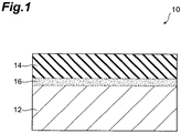
- Fig. 1 is a schematic sectional view showing the structure of a dielectric device 10 in accordance with an embodiment of the present invention.
- the dielectric device 10 has a base 12 which is a first conductor and a dielectric film 14 provided on the base 12.
- the base 12 is a conductor layer constituted by a conductive material.
- the dielectric film 14 is a dielectric constituted by a dielectric material.
- the base 12 is an Ni foil, whereas the dielectric film 14 is constituted by BST, i.e., barium strontium titanate (BaSr)TiO 3 .
- the base 12 has such a thickness as to be able to support the dielectric film 14 and maintain a sufficient strength.
- the thickness of the base 12 is about 100 ⁇ m, whereas the thickness of the dielectric film 14 is about 500 nm.
- Metal foils such as Ni foils are self-supportable and can favorably be used as the base 12 for supporting the dielectric film 14.
- An intermediate region 16 is formed between the base 12 and dielectric film 14.
- an additive different from Ni constituting the base 12 and BST constituting the dielectric film 14 is mixed with BST.
- the additive enhances the adhesion of the dielectric film 14 to the base 12.
- the additive is contained in the intermediate region 16 by a concentration sufficient for enhancing the adhesion of the dielectric film 14 by at least 1.5 times.
- an Ni foil made by rolling is prepared as the base 12.
- the method of making the metal foil for the base 12 in the present invention is not limited to rolling, but may be any of other methods such as electrolysis.
- the Ni foil used in this embodiment is doped with a sufficient amount of Si. Though the Ni foil is also doped with other elements such as Ti, Mg, Al, and P, Si has the highest concentration. Preferably, these additives have such a concentration as to enhance the critical peeling load value of the dielectric film 14 measured by scratching, which will be explained later, by at least 1.5 times. Preferred concentrations of the additives will be explained later in detail.
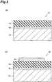
- a BST thin film is formed as the dielectric film 14 on the base 12, so as to make a multilayer structure 15.
- BST is deposited by sputtering on the base 12, so as to form the dielectric film 14.
- the method of forming the dielectric film 14 is not limited to sputtering in the present invention, whereby the dielectric film 14 may be formed by any of other methods such as chemical solution methods.
- the composition of BST is Ba 0 . 7 Sr 0 . 3 TiO 3 .
- the composition ratio between Ba and Sr is not limited to 7:3, whereby any other composition ratios can be employed.
- the multilayer structure 15 is introduced into an annealing furnace 20, and is heated in a high-temperature gas atmosphere 25 for a predetermined time.
- This annealing process improves the crystallinity of the dielectric film 14, while forming the intermediate region 16 on the boundary between the base 12 and dielectric film 14 ( Fig. 3(d) ).
- the annealing process causes the additives in the base 12 to flocculate into BST constituting the dielectric film 14, whereby the intermediate region 16 is formed. Therefore, in the intermediate region 16, the additives are mixed with BST.
- the atmosphere 25 For preventing the base 12, i.e., Ni foil, from being oxidized, a reducing atmosphere, a reduced-pressure atmosphere, or a reduced-pressure reducing atmosphere is used as the atmosphere 25.
- the reduced-pressure reducing atmosphere refers to a reducing atmosphere having a pressure lower than 1 atm.
- the temperature of the atmosphere 25 is 400°C or higher. In this embodiment, the temperature of the atmosphere 25 is set to 800°C.
- the intermediate region 16 completes the dielectric device 10.
- the intermediate region 16 may exist on the whole or a part of the boundary between the base 12 and dielectric film 14.
- the additives in the Ni foil may bind to oxygen when flocculated into the intermediate region 16. Therefore, there is a strong possibility that at least a part of the additives in the intermediate region 16 exists as an oxide.
- Fig. 4 is a photograph of a cross section taken with the TEM, whereas Figs. 5 and 6 show distributions of elements measured at the same cross section.
- Fig. 5 (a), (b), (c), and (d) indicate distributions of Ba, Ti, Sr, and Si, respectively.
- Fig. 6 (e), (f), (g), and (h) indicate distributions of Ni, P, Al, and O, respectively.
- regions where the respective elements exist are represented by white spots.
- Ni which is a main ingredient of the base 12 hardly exists, while the elements in BST are mixed with Si, P, and Al which are additives in the Ni foil.
- O is distributed over the whole area of the intermediate region, whereby major parts of Si, P, and Al seem to bind to 0, so as to form oxides.
- Fig. 7 is a photograph of a cross section enlarging a part of the intermediate region 16 in Fig. 5
- Fig. 8 shows distributions of elements measured at the same cross section.
- (i), (j), (k) and (1) indicate distributions of Ba, Ti, Sr, and Si, respectively.
- regions where the respective elements exist are represented by white spots.
- Si is distributed substantially uniformly without segregation as with the elements in BST. Therefore, Si and BST seem to react with each other in at least a part of the intermediate region 16.
- a thin-film capacitor is made in this embodiment.
- the thin-film capacitor is also one of dielectric devices. Specifically, as shown in Fig. 3(e) , an upper electrode 18 is formed on the dielectric film 14, so as to yield a thin-film capacitor 30.
- the upper electrode 18 is constituted by Cu.
- the base 12 made of the Ni foil functions as a lower electrode of the thin-film capacitor 30.
- the inventors By preparing a plurality of Ni rolled foils doped with various concentrations of Si, the inventors manufactured a plurality of dielectric devices 10 and thin-film capacitors 30, and measured the adhesion of the dielectric film 14 and electric characteristics of the thin-film capacitor 30, i.e., capacity density (C/A) and leak characteristic, in each of them.
- the capacity density is defined by (capacitance of thin-film capacitor 30)/(area of electrode 18).
- the adhesion of the dielectric film 14 was measured by using the dielectric device 10 instead of the thin-film capacitor 30.
- the measurement was conducted by scratching with an ultrathin film scratch tester CSR-02 of Rhesca Co., Ltd.
- the scratching is a method in which a hard indenter having a fixed radius of curvature is pressed against a surface of a film to be measured and scratches the surface of the film while increasing the load applied to the indenter, and a load value at which destruction of the film (e.g., peeling of the film from its backing material) occurs is measured. This load value is referred to as "critical peeling load value".
- R is the radius of curvature of the indenter
- H is the Brinell hardness of the backing material.
- Table 1 shows the results of measurement of critical peeling load values of the dielectric films 14 and electric characteristics of the thin-film capacitors 30.
- Table 1 Si concentration critical peeling load value C/A leak characteristic (ppm) (mN) ( ⁇ F/cm 2 ) (A/cm 2 ) 0 10 3.5 1.7 ⁇ 10 -7 10 15 3.5 1.7 ⁇ 10 -7 100 20 3.5 1.8 ⁇ 10 -7 500 23 3.5 2.0 ⁇ 10 -7 1000 23 3.5 2.2 ⁇ 10 -7 5000 25 3.0 2.8 ⁇ 10 -7 10000 25 2.4 3.4 ⁇ 10 -5
- leak characteristic indicates the current density of the leak current occurring when applying a voltage of 3 V between the lower electrode (i.e., base 12) and upper electrode 18 of the thin-film capacitor 30 at room temperature.
- Si concentration indicates the concentration of the simple substance of Si added to the Ni foil or the value obtained by converting the concentration of oxides of Si into the concentration of Si.
- the critical peeling load value of the dielectric film 14 was 10 mN when the concentration of Si added to the Ni foil was 0, i.e., when the Ni foil was doped with no Si, so that no Si existed in the intermediate region 16.
- the critical peeling load value was 15 mN, thus increasing by 1.5 times that obtained when the Si concentration was 0.
- the critical peeling load value increased, whereby a critical peeling load value of 25 mN was obtained at Si concentrations of 5000 ppm and 10000 ppm.
- the Si concentration exceeding 5000 ppm deteriorates electric characteristics of the thin-film capacitor 30 (more specifically, its capacity density (C/A) and leak characteristic), though the critical peeling load value of the dielectric film 14 is high. This seems to be because Si and oxides of Si diffuse into the dielectric film 14, and partly react with BST as the case may be, thereby deteriorating properties of BST as a dielectric.
- Fig. 9 is a schematic view showing distributions of additives measured by the EPMA.
- Fig. 9(a) shows the distribution of Si, in which a white region 22 indicates an area with a low Si concentration, whereas a region 26 with spots indicates an area with a high Si concentration.
- Fig. 9(a) shows the distribution of Si, in which a white region 22 indicates an area with a low Si concentration, whereas a region 26 with spots indicates an area with a high Si concentration.
- FIG. 9(b) shows the distribution of Al, in which a white region 23 indicates an area with a low A1 concentration, whereas a region 27 with spots indicates an area with a high A1 concentration.
- Fig. 9(c) shows the distribution of P, in which a white region 24 indicates an area with a low P concentration, whereas a region 28 with spots indicates an area with a high P concentration.
- Fig. 9 clarifies that additives are deposited on the surface of the Ni foil by the annealing process mentioned above and that the additives have nonuniform distributions on the surface of the Ni foil.
- P is distributed linearly along crystal grain boundaries of Ni.
- Fig. 9 shows Si, Al, and P among the additives in the Ni foil, other additives were also deposited on the surface of the Ni foil according to results of the analysis. There is a possibility of irregularities having been formed on the surface of the Ni foil because of the nonuniform distributions of additives (impurities).
- the concentration of Si in the Ni foil is 10 ppm to 5000 ppm in the dielectric device 10 and thin-film capacitor 30.
- the adhesion between the base 12 and dielectric film 14 is hard to enhance sufficiently when the concentration of Si in the Ni foil is less than 10 ppm, whereas the deterioration in electric characteristics of the thin-film capacitor 30 becomes remarkable when the Si concentration exceeds 5000 ppm.
- the Si concentration falling within the range of 10 to 5000 ppm can sufficiently improve the adhesion of the dielectric film 14 while yielding favorable electric characteristics.
- a more preferred concentration of Si is 100 ppm to 1000 ppm.
- the critical peeling load value of the dielectric film 14 can be enhanced by 2 times or more when the Si concentration in the Ni foil is at least 100 ppm.
- the Si concentration of 1000 ppm or less in the Ni foil can prevent the capacity density (C/A) from deteriorating.
- the dielectric device 10 and thin-film capacitor 30 in accordance with this embodiment have the intermediate region 16 containing Si as an additive, the adhesion of the dielectric film 14 is improved.
- the Si concentration is appropriately adjusted, favorable electric characteristics of the thin-film capacitor 30 can be obtained while keeping a high adhesion of the dielectric film 14.
- the intermediate region 16 formed at the boundary between the conductor and dielectric may contain at least one element selected from the group consisting of Al, P, Mg, Mn, Y, V, Mo, Co, Nb, Fe, and Cr. These elements may also be added to the backing material (base 12 in the above-mentioned embodiment) of the dielectric.
- Tables 2 to 12 show results of measurement of the critical peeling load value of the dielectric film 14 and electric characteristics of the thin-film capacitor 30 in the respective cases where the intermediate region 16 contains the above-mentioned elements.
- the method of measurement is as mentioned above in connection with Table 1.
- the "concentration" of each element represents the concentration of the simple substance of the element in the first conductor or the value obtained by converting the concentration of oxides of the element into the concentration of the element. All the elements are found to yield favorable critical peeling load values and electric characteristics of the thin-film capacitors 30 in the appropriate concentration range.
- the backing material (base 12 in the above-mentioned embodiment) of the dielectric is not limited to Ni, but may be constituted by Cu or A1 or an alloy mainly composed of Ni, Cu, or Al.
- the dielectric is not limited to BST.
- the dielectric may be an oxide, a preferred example of which is an oxide of perovskite type having a composition represented by a general formula of ABO 3 .
- Examples of the perovskite type oxide include oxides containing at least one element selected from the group consisting of Ba, Sr, Ca, Pb, Ti, Zr, and Hf.
- perovskite type oxide examples include BT, i.e., barium titanate BaTiO 3 , strontium titanate SrTiO 3 , (BaSr)(TiZr)O 3 , and BaTiZrO 3 in addition to BST.
- the dielectric may contain one or more of these oxides.
- the upper electrode 18 may be constituted by metals other than Cu (e.g., Pt) or alloys as well.
- the base 12 supporting the dielectric film 14 also acts as the lower electrode of the thin-film capacitor 30.
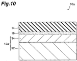
- a substrate 32 supporting a conductor layer 34 which is a first conductor and a dielectric film 14 may be provided as a base instead.
- Fig. 10 is a schematic sectional view showing thus modified dielectric device 10a.
- the substrate 32 has a sufficient thickness, and supports the conductor layer 34 and dielectric film 14.
- a layer 12a constituted by the substrate 32 and dielectric layer 34 functions as a base for supporting the dielectric film 14.
- the conductor layer 34 functions as a lower electrode.
- the present invention can provide a multilayer structure multilayer structure device which is excellent in adhesion between the conductor and dielectric, and a method of manufacturing the same.
Landscapes
- Engineering & Computer Science (AREA)
- Power Engineering (AREA)
- Microelectronics & Electronic Packaging (AREA)
- Manufacturing & Machinery (AREA)
- Chemical & Material Sciences (AREA)
- Materials Engineering (AREA)
- Fixed Capacitors And Capacitor Manufacturing Machines (AREA)
- Ceramic Capacitors (AREA)
- Inorganic Insulating Materials (AREA)
Claims (10)
- Élément à structure multicouche (10) comprenant :- une couche métallique (12) ;- une couche diélectrique (14) disposée sur la couche métallique (12) et constituée d'un matériau diélectrique ; et- une région intermédiaire (16) située entre la couche métallique (12) et la couche diélectrique (14),caractérisé en ce que
la couche métallique (12) comprend un additif choisi dans le groupe d'éléments comprenant Si, Al, P, Mg, Mn, Y, V, Mo, Co, Nb, Fe ou Cr,
la région intermédiaire (16) comprend ledit matériau diélectrique et ledit additif, et
la couche métallique (12) comprend ledit additif à une concentration de 10 ppm à 5 000 ppm quand l'élément est Si, et à une concentration de 10 ppm à 3 000 ppm quand l'élément est Al, P, Mg, Mn, Y, V, Mo, Co, Nb, Fe ou Cr. - Élément à structure multicouche (10) selon la revendication 1, la couche métallique (12) étant constituée de Ni, Cu ou Al ou d'un alliage principalement composé de quelconques éléments parmi ceux-ci.
- Élément à structure multicouche (10) selon la revendication 1, l'additif contenant un oxyde dudit élément.
- Élément à structure multicouche (10) selon la revendication 1, comprenant, en outre, une électrode supérieure (18) disposée sur la couche diélectrique (14).
- Élément à structure multicouche (10) selon la revendication 1, la couche métallique (12) étant constituée de Ni et Si à une concentration de 10 ppm à 5 000 ppm.
- Élément à structure multicouche (10) selon la revendication 1, la couche diélectrique (14) étant un oxyde.
- Élément à structure multicouche (10) selon la revendication 6, la couche diélectrique (14) ayant une structure perovskite et contenant au moins un élément choisi dans le groupe constitué de Ba, Sr, Ca, Pb, Ti, Zr et Hf.
- Élément à structure multicouche (10) selon la revendication 1, comprenant, en outre, une base destinée à servir de support à la couche métallique (12) et la couche diélectrique (14).
- Procédé de fabrication d'un élément à structure multicouche (10), le procédé comprenant les étapes consistant à :préparer une couche métallique (12) ;fournir une couche diélectrique (14) constituée d'un matériau différent de l'additif sur la couche métallique (12) ; etchauffer la couche métallique (12) et la couche diélectrique (14) afin de former une région intermédiaire (16) entre la couche métallique (12) et la couche diélectrique (14)caractérisé en ce que
la couche métallique (12) comprend un additif choisi dans le groupe d'éléments constitué de Si, Al, P, Mg, Mn, Y, V, Mo, Co, Nb, Fe ou Cr, ledit additif étant présent à une concentration de 10 ppm à 5 000 ppm quand l'élément est Si, et ledit additif étant présent à une concentration de 10 ppm à 3 000 ppm quand l'élément est Al, P, Mg, Mn, Y, V, Mo, Co, Nb, Fe ou Cr. - Procédé selon la revendication 9, la couche métallique (12) étant constituée de Ni et Si à une concentration de 10 ppm à 5 000 ppm.
Applications Claiming Priority (2)
| Application Number | Priority Date | Filing Date | Title |
|---|---|---|---|
| JP2005366715 | 2005-12-20 | ||
| JP2006309590A JP2007194592A (ja) | 2005-12-20 | 2006-11-15 | 誘電体素子とその製造方法 |
Publications (2)
| Publication Number | Publication Date |
|---|---|
| EP1801823A1 EP1801823A1 (fr) | 2007-06-27 |
| EP1801823B1 true EP1801823B1 (fr) | 2016-05-25 |
Family
ID=37836732
Family Applications (1)
| Application Number | Title | Priority Date | Filing Date |
|---|---|---|---|
| EP06026321.7A Ceased EP1801823B1 (fr) | 2005-12-20 | 2006-12-19 | Element multicouche et son procédé de fabrication |
Country Status (6)
| Country | Link |
|---|---|
| US (2) | US7808769B2 (fr) |
| EP (1) | EP1801823B1 (fr) |
| JP (1) | JP2007194592A (fr) |
| KR (1) | KR101238754B1 (fr) |
| CN (1) | CN1988084B (fr) |
| TW (1) | TW200735146A (fr) |
Families Citing this family (8)
| Publication number | Priority date | Publication date | Assignee | Title |
|---|---|---|---|---|
| JP5267251B2 (ja) * | 2008-03-31 | 2013-08-21 | Tdk株式会社 | 薄膜コンデンサ、及び薄膜コンデンサの製造方法 |
| JP5267265B2 (ja) * | 2009-03-25 | 2013-08-21 | Tdk株式会社 | 誘電体素子及び誘電体素子の製造方法 |
| EP2588851B1 (fr) | 2010-06-30 | 2016-12-21 | Life Technologies Corporation | Circuit d'accumulation de charge sensible aux ions et procédé associé |
| CN103513113B (zh) * | 2012-06-28 | 2017-03-01 | 联想(北京)有限公司 | 一种信息获取方法、设备及电容 |
| CN103151168B (zh) * | 2013-03-01 | 2016-01-06 | 溧阳华晶电子材料有限公司 | 一种薄膜电容器用镍基板 |
| JP6690154B2 (ja) * | 2015-09-02 | 2020-04-28 | Tdk株式会社 | 薄膜キャパシタ |
| KR102225451B1 (ko) | 2019-06-28 | 2021-03-09 | 삼성전기주식회사 | 유전체 조성물 및 이를 포함하는 적층형 전자 부품 |
| CN117177554A (zh) * | 2022-05-23 | 2023-12-05 | 华为技术有限公司 | 电子器件、芯片、电路板和电子设备 |
Family Cites Families (24)
| Publication number | Priority date | Publication date | Assignee | Title |
|---|---|---|---|---|
| DE1022957B (de) | 1952-11-26 | 1958-01-16 | Gulton Mfg Corp | Verfahren zum Herstellen einer flaechigen, elektrisch leitfaehigen Verbindung eines metallischen mit einem keramischen Werkstueck |
| US3678570A (en) * | 1971-04-01 | 1972-07-25 | United Aircraft Corp | Diffusion bonding utilizing transient liquid phase |
| US3769619A (en) * | 1972-04-20 | 1973-10-30 | Northrop Corp | Stripline assembly for use in microwave circuits and method of fabricating same |
| JP2884601B2 (ja) * | 1989-07-04 | 1999-04-19 | 富士通株式会社 | ベクトルプロセッサ |
| JPH0756850B2 (ja) * | 1989-09-29 | 1995-06-14 | 太陽誘電株式会社 | セラミック積層コンデンサおよびその製法 |
| JP2847680B2 (ja) * | 1990-03-26 | 1999-01-20 | 株式会社村田製作所 | セラミック電子部品及びその製造方法 |
| JPH0582589A (ja) * | 1991-09-20 | 1993-04-02 | Toshiba Corp | Tab用テープ |
| US5406447A (en) * | 1992-01-06 | 1995-04-11 | Nec Corporation | Capacitor used in an integrated circuit and comprising opposing electrodes having barrier metal films in contact with a dielectric film |
| US5587870A (en) * | 1992-09-17 | 1996-12-24 | Research Foundation Of State University Of New York | Nanocrystalline layer thin film capacitors |
| TW225044B (fr) * | 1992-11-20 | 1994-06-11 | Philips Electronics Nv | |
| US5645976A (en) * | 1993-10-14 | 1997-07-08 | Matsushita Electronics Corporation | Capacitor apparatus and method of manufacture of same |
| JP3291552B2 (ja) * | 1994-05-30 | 2002-06-10 | 独立行政法人産業技術総合研究所 | シール又は軸受 |
| CN1241030A (zh) * | 1998-07-02 | 2000-01-12 | 三星电子株式会社 | 高电介质电容器及其制造方法 |
| CA2289239C (fr) * | 1998-11-23 | 2010-07-20 | Micro Coating Technologies | Formation de condensateurs a film mince |
| DE19902769A1 (de) | 1999-01-25 | 2000-07-27 | Philips Corp Intellectual Pty | Keramisches, passives Bauelement |
| JP3838827B2 (ja) * | 1999-10-05 | 2006-10-25 | 新光電気工業株式会社 | 薄膜コンデンサ素子及びプリント回路基板の製造方法 |
| JP3630367B2 (ja) | 1999-11-12 | 2005-03-16 | 松下電器産業株式会社 | 回路基板および回路基板の製造方法 |
| US6407929B1 (en) * | 2000-06-29 | 2002-06-18 | Intel Corporation | Electronic package having embedded capacitors and method of fabrication therefor |
| US6700771B2 (en) * | 2001-08-30 | 2004-03-02 | Micron Technology, Inc. | Decoupling capacitor for high frequency noise immunity |
| TWI223291B (en) | 2001-10-25 | 2004-11-01 | Matsushita Electric Industrial Co Ltd | Laminated ceramic electronic component and method of manufacturing the same |
| UA77459C2 (en) * | 2001-11-03 | 2006-12-15 | Thin-film capacitor and a method for producing the capacitor | |
| JP3986859B2 (ja) * | 2002-03-25 | 2007-10-03 | 富士通株式会社 | 薄膜キャパシタ及びその製造方法 |
| WO2004070834A1 (fr) * | 2003-02-03 | 2004-08-19 | Koninklijke Philips Electronics N.V. | Procede de fabrication d'un dispositif a semiconducteur et dispositif a semiconducteur obtenu selon ce procede |
| JP3841814B1 (ja) | 2005-04-28 | 2006-11-08 | 三井金属鉱業株式会社 | キャパシタ層形成材及びそのキャパシタ層形成材の製造方法 |
-
2006
- 2006-11-15 JP JP2006309590A patent/JP2007194592A/ja active Pending
- 2006-12-13 US US11/637,709 patent/US7808769B2/en active Active
- 2006-12-19 EP EP06026321.7A patent/EP1801823B1/fr not_active Ceased
- 2006-12-19 TW TW095147645A patent/TW200735146A/zh unknown
- 2006-12-20 CN CN2006101692202A patent/CN1988084B/zh not_active Expired - Fee Related
- 2006-12-20 KR KR1020060130771A patent/KR101238754B1/ko not_active Expired - Fee Related
-
2010
- 2010-08-25 US US12/868,425 patent/US8468693B2/en not_active Expired - Fee Related
Also Published As
| Publication number | Publication date |
|---|---|
| CN1988084B (zh) | 2012-11-28 |
| US7808769B2 (en) | 2010-10-05 |
| TW200735146A (en) | 2007-09-16 |
| EP1801823A1 (fr) | 2007-06-27 |
| CN1988084A (zh) | 2007-06-27 |
| US8468693B2 (en) | 2013-06-25 |
| US20070138128A1 (en) | 2007-06-21 |
| US20100323097A1 (en) | 2010-12-23 |
| JP2007194592A (ja) | 2007-08-02 |
| KR20070065835A (ko) | 2007-06-25 |
| KR101238754B1 (ko) | 2013-03-06 |
Similar Documents
| Publication | Publication Date | Title |
|---|---|---|
| US8468693B2 (en) | Dielectric device and method of manufacturing the same | |
| KR102584977B1 (ko) | 세라믹 전자 부품 및 그 제조 방법 | |
| DE69017802T2 (de) | Dünnfilmkondensator und dessen Herstellungsverfahren. | |
| US12243691B2 (en) | Ceramic electronic device | |
| EP0814486B1 (fr) | Composition diélectrique céramique et son utilisation dans un condensateur monolithique céramique | |
| JP6015159B2 (ja) | 薄膜コンデンサ | |
| KR20220088099A (ko) | 세라믹 전자 부품 | |
| US12278053B2 (en) | Ceramic electronic component | |
| US11062847B2 (en) | Capacitor component and method for manufacturing the same | |
| KR20220101911A (ko) | 적층형 전자 부품 | |
| EP4113552B1 (fr) | Condensateur ceramique comprenant deux taille de grains cristallins a base de titanate de barium et d'additif | |
| JP7480459B2 (ja) | セラミック電子部品およびその製造方法 | |
| EP1770725B1 (fr) | Procédé de préparation d'un film diélectrique et condensateur associé | |
| EP2557578A1 (fr) | Procédé de fabrication d'une structure d'électrode, structure d'électrode et condensateur | |
| EP2772954A2 (fr) | Élément diélectrique et son procédé ce fabrication | |
| US8435645B2 (en) | Dielectric device and method of manufacturing dielectric device | |
| EP1497838B1 (fr) | Procédé pour la fabrication d'un composant ptc | |
| JP2001015376A (ja) | 積層セラミックコンデンサ | |
| US20070081297A1 (en) | Method of manufacturing thin film capacitor and printed circuit board having thin film capacitor embedded therein | |
| JP2022049235A (ja) | 誘電体薄膜素子および電子回路装置 | |
| EP4668302A1 (fr) | Composant électronique multicouche et son procédé de fabrication | |
| JPH01225148A (ja) | 誘電体薄膜及びその製造方法 | |
| JP4635936B2 (ja) | 誘電体素子およびその製造方法 | |
| EP3915961A1 (fr) | Condensateur | |
| KR20240133208A (ko) | 적층형 전자 부품 |
Legal Events
| Date | Code | Title | Description |
|---|---|---|---|
| PUAI | Public reference made under article 153(3) epc to a published international application that has entered the european phase |
Free format text: ORIGINAL CODE: 0009012 |
|
| AK | Designated contracting states |
Kind code of ref document: A1 Designated state(s): AT BE BG CH CY CZ DE DK EE ES FI FR GB GR HU IE IS IT LI LT LU LV MC NL PL PT RO SE SI SK TR |
|
| AX | Request for extension of the european patent |
Extension state: AL BA HR MK YU |
|
| 17P | Request for examination filed |
Effective date: 20071008 |
|
| 17Q | First examination report despatched |
Effective date: 20071108 |
|
| AKX | Designation fees paid |
Designated state(s): DE FR GB |
|
| RAP1 | Party data changed (applicant data changed or rights of an application transferred) |
Owner name: TDK CORPORATION |
|
| RAP1 | Party data changed (applicant data changed or rights of an application transferred) |
Owner name: TDK CORPORATION |
|
| REG | Reference to a national code |
Ref country code: DE Ref legal event code: R079 Ref document number: 602006049172 Country of ref document: DE Free format text: PREVIOUS MAIN CLASS: H01G0004008000 Ipc: H01G0004330000 |
|
| RIC1 | Information provided on ipc code assigned before grant |
Ipc: H05K 3/38 20060101ALI20151109BHEP Ipc: H01G 4/33 20060101AFI20151109BHEP |
|
| RIN1 | Information on inventor provided before grant (corrected) |
Inventor name: HORINO, KENJI Inventor name: KATOH, TOMOHIKO Inventor name: SAYA, YUKO |
|
| GRAP | Despatch of communication of intention to grant a patent |
Free format text: ORIGINAL CODE: EPIDOSNIGR1 |
|
| INTG | Intention to grant announced |
Effective date: 20160204 |
|
| GRAS | Grant fee paid |
Free format text: ORIGINAL CODE: EPIDOSNIGR3 |
|
| GRAA | (expected) grant |
Free format text: ORIGINAL CODE: 0009210 |
|
| AK | Designated contracting states |
Kind code of ref document: B1 Designated state(s): DE FR GB |
|
| REG | Reference to a national code |
Ref country code: GB Ref legal event code: FG4D |
|
| REG | Reference to a national code |
Ref country code: DE Ref legal event code: R096 Ref document number: 602006049172 Country of ref document: DE |
|
| REG | Reference to a national code |
Ref country code: FR Ref legal event code: PLFP Year of fee payment: 11 |
|
| REG | Reference to a national code |
Ref country code: DE Ref legal event code: R097 Ref document number: 602006049172 Country of ref document: DE |
|
| PLBE | No opposition filed within time limit |
Free format text: ORIGINAL CODE: 0009261 |
|
| STAA | Information on the status of an ep patent application or granted ep patent |
Free format text: STATUS: NO OPPOSITION FILED WITHIN TIME LIMIT |
|
| 26N | No opposition filed |
Effective date: 20170228 |
|
| REG | Reference to a national code |
Ref country code: FR Ref legal event code: PLFP Year of fee payment: 12 |
|
| P01 | Opt-out of the competence of the unified patent court (upc) registered |
Effective date: 20230512 |
|
| PGFP | Annual fee paid to national office [announced via postgrant information from national office to epo] |
Ref country code: GB Payment date: 20231102 Year of fee payment: 18 |
|
| PGFP | Annual fee paid to national office [announced via postgrant information from national office to epo] |
Ref country code: FR Payment date: 20231108 Year of fee payment: 18 Ref country code: DE Payment date: 20231031 Year of fee payment: 18 |
|
| REG | Reference to a national code |
Ref country code: DE Ref legal event code: R119 Ref document number: 602006049172 Country of ref document: DE |
|
| GBPC | Gb: european patent ceased through non-payment of renewal fee |
Effective date: 20241219 |
|
| PG25 | Lapsed in a contracting state [announced via postgrant information from national office to epo] |
Ref country code: DE Free format text: LAPSE BECAUSE OF NON-PAYMENT OF DUE FEES Effective date: 20250701 |
|
| PG25 | Lapsed in a contracting state [announced via postgrant information from national office to epo] |
Ref country code: GB Free format text: LAPSE BECAUSE OF NON-PAYMENT OF DUE FEES Effective date: 20241219 |
|
| PG25 | Lapsed in a contracting state [announced via postgrant information from national office to epo] |
Ref country code: FR Free format text: LAPSE BECAUSE OF NON-PAYMENT OF DUE FEES Effective date: 20241231 |