EP1808731A2 - Appareil, système et procédé d'impression - Google Patents
Appareil, système et procédé d'impression Download PDFInfo
- Publication number
- EP1808731A2 EP1808731A2 EP06024044A EP06024044A EP1808731A2 EP 1808731 A2 EP1808731 A2 EP 1808731A2 EP 06024044 A EP06024044 A EP 06024044A EP 06024044 A EP06024044 A EP 06024044A EP 1808731 A2 EP1808731 A2 EP 1808731A2
- Authority
- EP
- European Patent Office
- Prior art keywords
- disk substrate
- stamper
- gel pad
- membrane
- imprint
- Prior art date
- Legal status (The legal status is an assumption and is not a legal conclusion. Google has not performed a legal analysis and makes no representation as to the accuracy of the status listed.)
- Withdrawn
Links
Images


Classifications
-
- G—PHYSICS
- G11—INFORMATION STORAGE
- G11B—INFORMATION STORAGE BASED ON RELATIVE MOVEMENT BETWEEN RECORD CARRIER AND TRANSDUCER
- G11B7/00—Recording or reproducing by optical means, e.g. recording using a thermal beam of optical radiation by modifying optical properties or the physical structure, reproducing using an optical beam at lower power by sensing optical properties; Record carriers therefor
- G11B7/24—Record carriers characterised by shape, structure or physical properties, or by the selection of the material
- G11B7/26—Apparatus or processes specially adapted for the manufacture of record carriers
-
- G—PHYSICS
- G03—PHOTOGRAPHY; CINEMATOGRAPHY; ANALOGOUS TECHNIQUES USING WAVES OTHER THAN OPTICAL WAVES; ELECTROGRAPHY; HOLOGRAPHY
- G03F—PHOTOMECHANICAL PRODUCTION OF TEXTURED OR PATTERNED SURFACES, e.g. FOR PRINTING, FOR PROCESSING OF SEMICONDUCTOR DEVICES; MATERIALS THEREFOR; ORIGINALS THEREFOR; APPARATUS SPECIALLY ADAPTED THEREFOR
- G03F7/00—Photomechanical, e.g. photolithographic, production of textured or patterned surfaces, e.g. printing surfaces; Materials therefor, e.g. comprising photoresists; Apparatus specially adapted therefor
- G03F7/0002—Lithographic processes using patterning methods other than those involving the exposure to radiation, e.g. by stamping
-
- B—PERFORMING OPERATIONS; TRANSPORTING
- B82—NANOTECHNOLOGY
- B82Y—SPECIFIC USES OR APPLICATIONS OF NANOSTRUCTURES; MEASUREMENT OR ANALYSIS OF NANOSTRUCTURES; MANUFACTURE OR TREATMENT OF NANOSTRUCTURES
- B82Y10/00—Nanotechnology for information processing, storage or transmission, e.g. quantum computing or single electron logic
-
- B—PERFORMING OPERATIONS; TRANSPORTING
- B82—NANOTECHNOLOGY
- B82Y—SPECIFIC USES OR APPLICATIONS OF NANOSTRUCTURES; MEASUREMENT OR ANALYSIS OF NANOSTRUCTURES; MANUFACTURE OR TREATMENT OF NANOSTRUCTURES
- B82Y40/00—Manufacture or treatment of nanostructures
-
- Y—GENERAL TAGGING OF NEW TECHNOLOGICAL DEVELOPMENTS; GENERAL TAGGING OF CROSS-SECTIONAL TECHNOLOGIES SPANNING OVER SEVERAL SECTIONS OF THE IPC; TECHNICAL SUBJECTS COVERED BY FORMER USPC CROSS-REFERENCE ART COLLECTIONS [XRACs] AND DIGESTS
- Y10—TECHNICAL SUBJECTS COVERED BY FORMER USPC
- Y10S—TECHNICAL SUBJECTS COVERED BY FORMER USPC CROSS-REFERENCE ART COLLECTIONS [XRACs] AND DIGESTS
- Y10S977/00—Nanotechnology
- Y10S977/84—Manufacture, treatment, or detection of nanostructure
- Y10S977/887—Nanoimprint lithography, i.e. nanostamp
Definitions
- the present invention relates in general to an imprinting apparatus, system and method and, in particular to nanoimprinting.
- Nanoimprinting technology has developed into a high profile technology that provides a pathway to the next generation of lithography.
- the features of nanoimprinting such as pillars, pits, and tracks, are on the order of about 10 nm in diameter and/or width.
- a master is typically used to generate the templates, and the templates are then used for mass imprinting production to avoid damage to the valuable master in any imprinting accident.
- the potentials for nanoimprinting in high throughput and low manufacturing cost could trigger a paradigm shift in today's optical lithography technology.
- FIG. 1 schematically illustrates a typical imprinting configuration that includes a mold/stamper/template 11 having a feature pattern 13 that forms imprinted features 15 in a resist layer 17 with a base layer 18 on a substrate 19.
- the base layer thickness and uniformity is the parameter that nanoimprinting technology tries to control and perfect. Because the imprinted resist layer is acting as a etch mask for the follow-up reactive ion etch (RIE) step in the nanoimprinting process, the quality of the base layer uniformity is directly linked to the quality of the etched result.
- RIE reactive ion etch
- Figure 2 depicts the differences in the uniformity of the base layer thickness even with the same fidelity of the imprinted pattern features.
- the top imprint 21 is sufficient for some applications (i.e., no further processing is required), such as in the compact disc (CD) or DVD stamping business, where good fidelity of the imprinted features is the only requirement and base layer uniformity is unnecessary. See, for example, Japanese Patent JP2004330680 .
- the uniformity of the base layer becomes critical and the uniformity of bottom imprint 23 is necessary.
- the bottom imprint 23 is only possible with further processing by etching through the imprint to directly transport the pattern to the substrate.
- Various types of nanoimprinting tooling have been developed and commercialized. Unfortunately, in order to achieve uniform imprinting pressure, either very complicated gimbaling fixtures or much higher imprinting pressure is typically employed.
- a conventional imprinting contact configuration comprises a substrate vacuum chuck 41 to which is mounted substrate 19.
- the stamper 11 is supported by a gel pad 43 and Mylar membrane 45 which extends across an opening in a fixture 47. Air pressure is applied to the membrane 45 to press the stamper 11 against substrate 19.
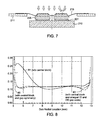
- this design produces an approximately 50% variation in contact pressure in the radial direction across the imprinted zone 55 with the gel pad (plot 51) or without the gel pad (plot 53).
- One embodiment of a system, method, and apparatus for nanoimprinting facilitates its own patterned media contact architecture to provide a uniform imprinting pressure across the entire imprinting area by configuring a membrane, pad, and stamper architecture.
- the present invention employs a significantly simpler but efficient fixture solution compared to prior art designs.
- the present invention leverages the unique disk substrate characteristic of an inner diameter (ID) hole.
- ID inner diameter
- This solution incorporates a membrane suspension, gel-pad buffering, and air cushion loading while exploiting the ID hole characteristics of the disk substrate to dramatically increase the uniformity of the pressing pressure across the target imprinting area. As a result, a simple and effective improvement of the quality of the patterns imprinted on the recording disk substrate is realized.
- the present invention may comprise an imprinting apparatus comprising a membrane stop ring having an opening; a membrane mounted to the membrane stop ring such that the membrane extends and seals across the opening in the membrane stop ring; a gel pad mounted to the membrane, the gel pad having a disk-like shape including an axial hole; a stamper mounted to the gel pad and having a disk-like shape including an axial hole, and a contact surface with imprint features; and a central block mounted to the membrane and extending through the axial holes of the gel pad and the stamper.
- the present invention comprises a disk substrate 101 having an outer diameter 103, an axial hole 105 that defines an inner diameter 107, and an imprint surface 109 extending in a radial direction.
- a chuck 110 such as a vacuum chuck, is used to support the disk substrate 101 opposite the imprint surface 109.
- the system further comprises a membrane stop ring 111 having an opening 113.
- a suspension mechanism or membrane 115 such as a Mylar membrane (e.g., approximately 30 ⁇ m thick), is mounted to the membrane stop ring 111 such that the membrane 115 extends and seals across the opening 113 in the membrane stop ring 111.
- a gel pad 117 is mounted to the membrane 115.
- the gel pad 117 which has a thickness of approximately 1 to 2 mm, is employed as a stress buffer and also an interlayer to hold a stamper 125.
- the gel pad 117 has an outer diameter 119 and an axial hole 121 that defines an inner diameter 123 such that the gel pad 117 is disk-like or cylindrical in shape and substantially congruent with the disk substrate 101.
- the stamper 125 is mounted to the gel pad 117.
- the stamper 125 has an outer diameter 126, and an axial hole 129 that defines an inner diameter 131 such that the stamper 125 is disk-like or cylindrical in shape and substantially congruent with the disk substrate 101.
- the stamper 125 also has a contact surface 127 with imprint features (see Figures 1 and 2) for imprinting a resist layer on the imprint surface 109 of the disk substrate 101.
- the contact surface 127 of the stamper 125 has a radial dimension (see Figure 6) that is less than a radial dimension of the disk substrate 101 between the inner and outer diameters 103, 107 of the disk substrate 101, such that a radial dimension of the imprint surface 109 of the disk substrate 101 is less than the radial dimension of the disk substrate 101 between the inner and outer diameters 103, 107 of the disk substrate 101.
- the gel pad 117 may have a radial dimension between its inner and outer diameters 123, 119 that is approximately equal to or slightly less than the radial dimension of the contact surface 127 of the stamper 125.
- the present invention also incorporates a central block 133 that is mounted to the membrane 115 and extends through the axial holes 121, 129, 105 of the gel pad 117, the stamper 125, and the disk substrate 101 into contact with the chuck 110.
- the central block 133 is cylindrical and extends in an axial direction concentric with the axial holes 121, 129, 105 of the gel pad 117, the stamper 125, and the disk substrate 101, respectively.
- the central block 133 has an axial length that is approximately equal to the sum of the axial lengths of the gel pad 117, the stamper 125, and the disk substrate 101. However, because of the flexibility of the membrane 115, some slight differences (either larger or smaller) will not significantly influence the pressure uniformity. In one embodiment, the central block 133 has an axial dimension that is greater than a combined axial dimension of the stamper 125 and the gel pad 117.
- the central block 133 has a radial dimension that is less than radial dimensions of the inner diameters 123, 131, 107 of the gel pad 117, the stamper 125, and the disk substrate 101, respectively, such that the central block 133 is free of contact with the gel pad 117, the stamper 125, and the disk substrate 101.
- the present invention further comprises one or more directional stages 141 (e.g., x, y, and z directions) and one or more rotational stages 143 for adjusting a position of the chuck 110.
- a load cell 145 and leveling mechanism 147 are located between the chuck 110 and the directional and rotational stages 141, 143.
- a quartz window 149 is located above the apparatus for exposing the disk substrate 101 to UV radiation.
- a sealed first chamber (or upper chamber) 151 is used for pressurizing the stamper 125 via membrane 115 (see arrows in Figure 6) by introducing air pressure in chamber 151 and thereby imprint on the disk substrate 101.
- a separate, sealed second chamber (or lower chamber) 153 contains the disk substrate 101, and may be evacuated or purged with an inert gas such as argon or nitrogen. The imprinting operation may be controlled by manipulating the pressures in the upper and lower chambers 151, 153 independently.
- the air inside the upper chamber 151 is first pumped out so that the vacuum suction force holds the membrane 115 together with the stamper 125 and gel pad 117 against the quartz window 149. This is the standby position of the stamper assembly.
- the upper chamber 151 is then gradually vented to ambient so as to carry on a "vacuum imprinting" or a lower pressure imprinting.
- These steps form a vacuum environment in the lower chamber 153 and are followed by a low pressure imprinting operation.
- the pressure range available in the vacuum imprinting scheme can be from 0 to about 10 psi in one embodiment.
- FIG. 7 an example of an imprinting system that does not utilize a central block is shown for comparison purposes.
- This example system is identical to that shown in Figure 6, including a disk substrate 201, a chuck 210, a stop 211, membrane 215, gel pad 217, and stamper 225.
- membrane 215 has no central block on which to exert pressure.
- the present invention also includes a method of nanoimprinting for achieving uniform imprint pressure.
- the method begins as illustrated at step 90, and comprises providing a stamper and a disk substrate having an outer diameter, an axial hole that defines an inner diameter, and an imprint surface extending in a radial direction (step 91); positioning a central block through an axial hole in the stamper (step 93); applying resist to the imprint surface of the disk substrate (step 95); pressurizing a stamper to imprint the resist layer on the imprint surface of the disk substrate with imprint features such that the central block is also pressurized (step 97); curing (e.g., via UV light) the imprint features followed by separation of the stamper and disk substrate (step 98), before ending as indicated at step 99.
- the imprinted resist layer left on the disk substrate has both imprint feature uniformity and base layer uniformity.
- the method may further comprise providing the central block with an axial dimension that is greater than a combined axial dimension of the stamper and a gel pad, and providing the central block with a radial dimension that is less than radial dimensions of inner diameters of the gel pad, the stamper, and the disk substrate, respectively, such that the central block is free of contact with the gel pad, the stamper, and the disk substrate.
- the method may further comprise directionally and rotationally adjusting the disk substrate, adjusting a load and a level of the disk substrate, and exposing the disk substrate to UV radiation.
Landscapes
- Engineering & Computer Science (AREA)
- Chemical & Material Sciences (AREA)
- Nanotechnology (AREA)
- Physics & Mathematics (AREA)
- General Physics & Mathematics (AREA)
- Crystallography & Structural Chemistry (AREA)
- Manufacturing & Machinery (AREA)
- Theoretical Computer Science (AREA)
- Condensed Matter Physics & Semiconductors (AREA)
- Mathematical Physics (AREA)
- Shaping Of Tube Ends By Bending Or Straightening (AREA)
- Manufacturing Of Magnetic Record Carriers (AREA)
- Exposure Of Semiconductors, Excluding Electron Or Ion Beam Exposure (AREA)
- Micromachines (AREA)
- Manufacturing Optical Record Carriers (AREA)
- Casting Or Compression Moulding Of Plastics Or The Like (AREA)
Applications Claiming Priority (1)
| Application Number | Priority Date | Filing Date | Title |
|---|---|---|---|
| US11/331,367 US7500431B2 (en) | 2006-01-12 | 2006-01-12 | System, method, and apparatus for membrane, pad, and stamper architecture for uniform base layer and nanoimprinting pressure |
Publications (2)
| Publication Number | Publication Date |
|---|---|
| EP1808731A2 true EP1808731A2 (fr) | 2007-07-18 |
| EP1808731A3 EP1808731A3 (fr) | 2009-12-02 |
Family
ID=37945843
Family Applications (1)
| Application Number | Title | Priority Date | Filing Date |
|---|---|---|---|
| EP06024044A Withdrawn EP1808731A3 (fr) | 2006-01-12 | 2006-11-20 | Appareil, système et procédé d'impression |
Country Status (6)
| Country | Link |
|---|---|
| US (2) | US7500431B2 (fr) |
| EP (1) | EP1808731A3 (fr) |
| JP (1) | JP5036322B2 (fr) |
| KR (1) | KR20070075275A (fr) |
| CN (1) | CN101000463B (fr) |
| TW (1) | TW200738427A (fr) |
Cited By (1)
| Publication number | Priority date | Publication date | Assignee | Title |
|---|---|---|---|---|
| EP1818721A3 (fr) * | 2006-02-14 | 2009-12-02 | Hitachi Global Storage Technologies Netherlands B.V. | Système, méthode et appareil pour exposition de durcissement diffus et sans contact pour la réalisation d'une matrice de nano-impression photopolymère |
Families Citing this family (15)
| Publication number | Priority date | Publication date | Assignee | Title |
|---|---|---|---|---|
| US7500431B2 (en) * | 2006-01-12 | 2009-03-10 | Tsai-Wei Wu | System, method, and apparatus for membrane, pad, and stamper architecture for uniform base layer and nanoimprinting pressure |
| JP4478164B2 (ja) * | 2007-03-12 | 2010-06-09 | 株式会社日立ハイテクノロジーズ | 微細構造転写装置、スタンパおよび微細構造の製造方法 |
| US20090056575A1 (en) * | 2007-08-31 | 2009-03-05 | Bartman Jon A | Pattern transfer apparatus |
| EP2058107B1 (fr) * | 2007-11-08 | 2012-08-08 | EV Group E. Thallner GmbH | Dispositif destiné à la structuration homogène de substrats |
| TWI342270B (en) * | 2008-07-15 | 2011-05-21 | Univ Nat Taiwan | Specific-light-cured and pressure-differential embossing apparatus |
| JP5182525B2 (ja) * | 2009-03-25 | 2013-04-17 | 株式会社Jvcケンウッド | 光ディスク製造方法及び光ディスク製造装置 |
| JP2010267357A (ja) * | 2009-05-18 | 2010-11-25 | Hitachi High-Technologies Corp | パターンドメディアの製造方法及び製造装置 |
| JP5883447B2 (ja) * | 2010-10-26 | 2016-03-15 | エーファウ・グループ・ゲーエムベーハー | レンズウエハーを製造するための方法および装置 |
| TWI409161B (zh) * | 2010-12-10 | 2013-09-21 | Chenming Mold Ind Corp | 均壓成型模具及其均壓成型方法 |
| CN102173238A (zh) * | 2010-12-29 | 2011-09-07 | 友达光电股份有限公司 | 真空压印装置、真空压合装置及层状光学组件的制造方法 |
| TWI627359B (zh) * | 2016-10-28 | 2018-06-21 | Diaphragm type operator and test classification equipment thereof | |
| CN108908642B (zh) * | 2018-08-20 | 2020-08-11 | 池家丰 | 一种导热纤维板及其加工方法 |
| CN109765687B (zh) * | 2018-12-04 | 2021-12-14 | 上海安翰医疗技术有限公司 | 曲面外壳上疏水涂层的制作方法及内窥镜 |
| JP6972409B1 (ja) * | 2021-03-30 | 2021-11-24 | リンテック株式会社 | マイクロニードルの製造方法およびマイクロニードルの製造装置 |
| JP2026503205A (ja) * | 2023-01-03 | 2026-01-28 | エーファウ・グループ・エー・タルナー・ゲーエムベーハー | 排気された加工室内で基板を加工する装置および方法 |
Family Cites Families (28)
| Publication number | Priority date | Publication date | Assignee | Title |
|---|---|---|---|---|
| JPS6180534A (ja) * | 1984-09-28 | 1986-04-24 | Toshiba Corp | 光デイスク基板の張り合せ方法 |
| DE3719200A1 (de) * | 1987-06-09 | 1988-12-29 | Ibm Deutschland | Optische speicherplatte und verfahren zu ihrer herstellung |
| JP2637147B2 (ja) * | 1988-03-22 | 1997-08-06 | 株式会社東芝 | 光ディスクの貼り合せ方法及び光ディスク貼り合せ装置 |
| JPH08106655A (ja) | 1992-02-29 | 1996-04-23 | Takeda Giken Kogyo:Kk | ディスクの製造方法及びディスクプレス装置 |
| JPH087346A (ja) | 1994-06-24 | 1996-01-12 | Hitachi Ltd | 密着治具及び密着方法 |
| US5804017A (en) * | 1995-07-27 | 1998-09-08 | Imation Corp. | Method and apparatus for making an optical information record |
| US5669303A (en) * | 1996-03-04 | 1997-09-23 | Motorola | Apparatus and method for stamping a surface |
| SE515607C2 (sv) * | 1999-12-10 | 2001-09-10 | Obducat Ab | Anordning och metod vid tillverkning av strukturer |
| JP3638514B2 (ja) | 2000-09-27 | 2005-04-13 | 株式会社東芝 | 転写装置、転写用カートリッジ、及び転写方法 |
| CN100365507C (zh) * | 2000-10-12 | 2008-01-30 | 德克萨斯州大学系统董事会 | 用于室温下低压微刻痕和毫微刻痕光刻的模板 |
| JP2002269853A (ja) | 2001-03-06 | 2002-09-20 | Sony Corp | 光ディスクの製造方法および光ディスクの製造装置 |
| JP2002304779A (ja) | 2001-04-05 | 2002-10-18 | Sony Corp | 光ディスク用スタンパーの製作方法 |
| JP3850718B2 (ja) * | 2001-11-22 | 2006-11-29 | 株式会社東芝 | 加工方法 |
| JP4061220B2 (ja) * | 2003-03-20 | 2008-03-12 | 株式会社日立製作所 | ナノプリント装置、及び微細構造転写方法 |
| JP4317375B2 (ja) * | 2003-03-20 | 2009-08-19 | 株式会社日立製作所 | ナノプリント装置、及び微細構造転写方法 |
| JP4155511B2 (ja) | 2003-05-09 | 2008-09-24 | Tdk株式会社 | インプリント装置およびインプリント方法 |
| WO2004100143A1 (fr) | 2003-05-09 | 2004-11-18 | Tdk Corporation | Dispositif et procede d'estampage |
| JP4185808B2 (ja) * | 2003-05-09 | 2008-11-26 | Tdk株式会社 | インプリント装置およびインプリント方法 |
| JP2004330680A (ja) | 2003-05-09 | 2004-11-25 | Tdk Corp | インプリント装置およびインプリント方法 |
| JP3889386B2 (ja) * | 2003-09-30 | 2007-03-07 | 株式会社東芝 | インプリント装置及びインプリント方法 |
| US7037458B2 (en) * | 2003-10-23 | 2006-05-02 | Intel Corporation | Progressive stamping apparatus and method |
| EP1538482B1 (fr) * | 2003-12-05 | 2016-02-17 | Obducat AB | Appareil et méthode pour lithograpie sur grandes surfaces |
| EP1594001B1 (fr) * | 2004-05-07 | 2015-12-30 | Obducat AB | Appareil et méthode pour la lithographie par empreinte |
| AU2005282060A1 (en) * | 2004-09-08 | 2006-03-16 | Nil Technology Aps | A flexible nano-imprint stamp |
| CN1292306C (zh) * | 2004-12-09 | 2006-12-27 | 上海交通大学 | 真空负压纳米压印装置 |
| WO2006131153A1 (fr) * | 2005-06-10 | 2006-12-14 | Obducat Ab | Reproduction de motif a tampon intermediaire |
| ATE549294T1 (de) * | 2005-12-09 | 2012-03-15 | Obducat Ab | Vorrichtung und verfahren zum transfer von mustern mit zwischenstempel |
| US7500431B2 (en) | 2006-01-12 | 2009-03-10 | Tsai-Wei Wu | System, method, and apparatus for membrane, pad, and stamper architecture for uniform base layer and nanoimprinting pressure |
-
2006
- 2006-01-12 US US11/331,367 patent/US7500431B2/en not_active Expired - Fee Related
- 2006-11-20 EP EP06024044A patent/EP1808731A3/fr not_active Withdrawn
- 2006-12-20 TW TW095147998A patent/TW200738427A/zh unknown
- 2006-12-29 KR KR1020060138161A patent/KR20070075275A/ko not_active Withdrawn
-
2007
- 2007-01-11 JP JP2007003419A patent/JP5036322B2/ja not_active Expired - Fee Related
- 2007-01-12 CN CN2007100021667A patent/CN101000463B/zh not_active Expired - Fee Related
-
2008
- 2008-10-27 US US12/258,767 patent/US7617769B2/en not_active Expired - Fee Related
Cited By (2)
| Publication number | Priority date | Publication date | Assignee | Title |
|---|---|---|---|---|
| EP1818721A3 (fr) * | 2006-02-14 | 2009-12-02 | Hitachi Global Storage Technologies Netherlands B.V. | Système, méthode et appareil pour exposition de durcissement diffus et sans contact pour la réalisation d'une matrice de nano-impression photopolymère |
| US7731889B2 (en) | 2006-02-14 | 2010-06-08 | Hitachi Global Storage Technologies Netherlands B.V. | Method for non-contact and diffuse curing exposure for making photopolymer nanoimprinting stamper |
Also Published As
| Publication number | Publication date |
|---|---|
| JP2007188626A (ja) | 2007-07-26 |
| CN101000463A (zh) | 2007-07-18 |
| TW200738427A (en) | 2007-10-16 |
| US20090045534A1 (en) | 2009-02-19 |
| EP1808731A3 (fr) | 2009-12-02 |
| JP5036322B2 (ja) | 2012-09-26 |
| CN101000463B (zh) | 2010-12-08 |
| US7617769B2 (en) | 2009-11-17 |
| US7500431B2 (en) | 2009-03-10 |
| KR20070075275A (ko) | 2007-07-18 |
| US20070158866A1 (en) | 2007-07-12 |
Similar Documents
| Publication | Publication Date | Title |
|---|---|---|
| US7617769B2 (en) | System, method, and apparatus for membrane, pad, and stamper architecture for uniform base layer and nanoimprinting pressure | |
| US7857611B2 (en) | Imprinting device and imprinting method | |
| JP4478164B2 (ja) | 微細構造転写装置、スタンパおよび微細構造の製造方法 | |
| US8215946B2 (en) | Imprint lithography system and method | |
| US7798801B2 (en) | Chucking system for nano-manufacturing | |
| US7636999B2 (en) | Method of retaining a substrate to a wafer chuck | |
| US8685306B2 (en) | Molding apparatus and molding method | |
| US20080204693A1 (en) | Substrate Support Method | |
| JP2006326927A (ja) | インプリント装置、及び微細構造転写方法 | |
| JP2005183985A (ja) | インプリント・リソグラフィのための複合スタンパ | |
| WO2011111441A1 (fr) | Procédé et dispositif de transfert de microstructure | |
| WO2011077882A1 (fr) | Dispositif d'empreinte double face | |
| CN105934711A (zh) | 用于改进的覆盖纠正的低接触式压印光刻术模板卡盘系统 | |
| US20070062396A1 (en) | Imprinting apparatus and imprinting method | |
| US8047835B2 (en) | Method of transcribing fine pattern and fine structure pattern transcription apparatus | |
| JP2006018977A (ja) | 転写印刷版用実装金型及び転写印刷方法 | |
| US8334967B2 (en) | Substrate support system having a plurality of contact lands | |
| US20100096775A1 (en) | Mold imprinting | |
| KR20250133650A (ko) | 배기된 처리 공간에서 기판을 처리하는 장치 및 방법 | |
| JP2013118233A (ja) | 微細構造転写装置 |
Legal Events
| Date | Code | Title | Description |
|---|---|---|---|
| PUAI | Public reference made under article 153(3) epc to a published international application that has entered the european phase |
Free format text: ORIGINAL CODE: 0009012 |
|
| AK | Designated contracting states |
Kind code of ref document: A2 Designated state(s): AT BE BG CH CY CZ DE DK EE ES FI FR GB GR HU IE IS IT LI LT LU LV MC NL PL PT RO SE SI SK TR |
|
| AX | Request for extension of the european patent |
Extension state: AL BA HR MK YU |
|
| PUAL | Search report despatched |
Free format text: ORIGINAL CODE: 0009013 |
|
| AK | Designated contracting states |
Kind code of ref document: A3 Designated state(s): AT BE BG CH CY CZ DE DK EE ES FI FR GB GR HU IE IS IT LI LT LU LV MC NL PL PT RO SE SI SK TR |
|
| AX | Request for extension of the european patent |
Extension state: AL BA HR MK RS |
|
| AKY | No designation fees paid | ||
| STAA | Information on the status of an ep patent application or granted ep patent |
Free format text: STATUS: THE APPLICATION IS DEEMED TO BE WITHDRAWN |
|
| 18D | Application deemed to be withdrawn |
Effective date: 20100601 |
|
| REG | Reference to a national code |
Ref country code: DE Ref legal event code: 8566 |