EP1811571A2 - Organische lichtemittierende Anzeigevorrichtung und Herstellungsverfahren - Google Patents
Organische lichtemittierende Anzeigevorrichtung und Herstellungsverfahren Download PDFInfo
- Publication number
- EP1811571A2 EP1811571A2 EP07250270A EP07250270A EP1811571A2 EP 1811571 A2 EP1811571 A2 EP 1811571A2 EP 07250270 A EP07250270 A EP 07250270A EP 07250270 A EP07250270 A EP 07250270A EP 1811571 A2 EP1811571 A2 EP 1811571A2
- Authority
- EP
- European Patent Office
- Prior art keywords
- conductive line
- frit
- substrate
- oxide
- seal
- Prior art date
- Legal status (The legal status is an assumption and is not a legal conclusion. Google has not performed a legal analysis and makes no representation as to the accuracy of the status listed.)
- Granted
Links
Images



Classifications
-
- H—ELECTRICITY
- H10—SEMICONDUCTOR DEVICES; ELECTRIC SOLID-STATE DEVICES NOT OTHERWISE PROVIDED FOR
- H10K—ORGANIC ELECTRIC SOLID-STATE DEVICES
- H10K59/00—Integrated devices, or assemblies of multiple devices, comprising at least one organic light-emitting element covered by group H10K50/00
- H10K59/80—Constructional details
- H10K59/87—Passivation; Containers; Encapsulations
- H10K59/871—Self-supporting sealing arrangements
- H10K59/8722—Peripheral sealing arrangements, e.g. adhesives, sealants
-
- A—HUMAN NECESSITIES
- A61—MEDICAL OR VETERINARY SCIENCE; HYGIENE
- A61M—DEVICES FOR INTRODUCING MEDIA INTO, OR ONTO, THE BODY; DEVICES FOR TRANSDUCING BODY MEDIA OR FOR TAKING MEDIA FROM THE BODY; DEVICES FOR PRODUCING OR ENDING SLEEP OR STUPOR
- A61M5/00—Devices for bringing media into the body in a subcutaneous, intra-vascular or intramuscular way; Accessories therefor, e.g. filling or cleaning devices, arm-rests
- A61M5/178—Syringes
- A61M5/31—Details
- A61M5/32—Needles; Details of needles pertaining to their connection with syringe or hub; Accessories for bringing the needle into, or holding the needle on, the body; Devices for protection of needles
- A61M5/3205—Apparatus for removing or disposing of used needles or syringes, e.g. containers; Means for protection against accidental injuries from used needles
- A61M5/321—Means for protection against accidental injuries by used needles
- A61M5/322—Retractable needles, i.e. disconnected from and withdrawn into the syringe barrel by the piston
- A61M5/3232—Semi-automatic needle retraction, i.e. in which triggering of the needle retraction requires a deliberate action by the user, e.g. manual release of spring-biased retraction means
-
- A—HUMAN NECESSITIES
- A61—MEDICAL OR VETERINARY SCIENCE; HYGIENE
- A61M—DEVICES FOR INTRODUCING MEDIA INTO, OR ONTO, THE BODY; DEVICES FOR TRANSDUCING BODY MEDIA OR FOR TAKING MEDIA FROM THE BODY; DEVICES FOR PRODUCING OR ENDING SLEEP OR STUPOR
- A61M5/00—Devices for bringing media into the body in a subcutaneous, intra-vascular or intramuscular way; Accessories therefor, e.g. filling or cleaning devices, arm-rests
- A61M5/178—Syringes
- A61M5/31—Details
- A61M5/32—Needles; Details of needles pertaining to their connection with syringe or hub; Accessories for bringing the needle into, or holding the needle on, the body; Devices for protection of needles
- A61M5/3205—Apparatus for removing or disposing of used needles or syringes, e.g. containers; Means for protection against accidental injuries from used needles
- A61M5/321—Means for protection against accidental injuries by used needles
- A61M5/322—Retractable needles, i.e. disconnected from and withdrawn into the syringe barrel by the piston
- A61M5/3221—Constructional features thereof, e.g. to improve manipulation or functioning
-
- A—HUMAN NECESSITIES
- A61—MEDICAL OR VETERINARY SCIENCE; HYGIENE
- A61M—DEVICES FOR INTRODUCING MEDIA INTO, OR ONTO, THE BODY; DEVICES FOR TRANSDUCING BODY MEDIA OR FOR TAKING MEDIA FROM THE BODY; DEVICES FOR PRODUCING OR ENDING SLEEP OR STUPOR
- A61M5/00—Devices for bringing media into the body in a subcutaneous, intra-vascular or intramuscular way; Accessories therefor, e.g. filling or cleaning devices, arm-rests
- A61M5/50—Devices for bringing media into the body in a subcutaneous, intra-vascular or intramuscular way; Accessories therefor, e.g. filling or cleaning devices, arm-rests having means for preventing re-use, or for indicating if defective, used, tampered with or unsterile
- A61M5/5066—Means for preventing re-use by disconnection of piston and piston-rod
-
- H—ELECTRICITY
- H10—SEMICONDUCTOR DEVICES; ELECTRIC SOLID-STATE DEVICES NOT OTHERWISE PROVIDED FOR
- H10K—ORGANIC ELECTRIC SOLID-STATE DEVICES
- H10K50/00—Organic light-emitting devices
- H10K50/80—Constructional details
- H10K50/84—Passivation; Containers; Encapsulations
- H10K50/842—Containers
- H10K50/8426—Peripheral sealing arrangements, e.g. adhesives, sealants
-
- A—HUMAN NECESSITIES
- A61—MEDICAL OR VETERINARY SCIENCE; HYGIENE
- A61M—DEVICES FOR INTRODUCING MEDIA INTO, OR ONTO, THE BODY; DEVICES FOR TRANSDUCING BODY MEDIA OR FOR TAKING MEDIA FROM THE BODY; DEVICES FOR PRODUCING OR ENDING SLEEP OR STUPOR
- A61M5/00—Devices for bringing media into the body in a subcutaneous, intra-vascular or intramuscular way; Accessories therefor, e.g. filling or cleaning devices, arm-rests
- A61M5/178—Syringes
- A61M5/31—Details
- A61M5/32—Needles; Details of needles pertaining to their connection with syringe or hub; Accessories for bringing the needle into, or holding the needle on, the body; Devices for protection of needles
- A61M5/3205—Apparatus for removing or disposing of used needles or syringes, e.g. containers; Means for protection against accidental injuries from used needles
- A61M2005/3206—Needle or needle hub disconnecting devices forming part of or being attached to the hub or syringe body
-
- A—HUMAN NECESSITIES
- A61—MEDICAL OR VETERINARY SCIENCE; HYGIENE
- A61M—DEVICES FOR INTRODUCING MEDIA INTO, OR ONTO, THE BODY; DEVICES FOR TRANSDUCING BODY MEDIA OR FOR TAKING MEDIA FROM THE BODY; DEVICES FOR PRODUCING OR ENDING SLEEP OR STUPOR
- A61M5/00—Devices for bringing media into the body in a subcutaneous, intra-vascular or intramuscular way; Accessories therefor, e.g. filling or cleaning devices, arm-rests
- A61M5/178—Syringes
- A61M5/31—Details
- A61M5/32—Needles; Details of needles pertaining to their connection with syringe or hub; Accessories for bringing the needle into, or holding the needle on, the body; Devices for protection of needles
- A61M5/3205—Apparatus for removing or disposing of used needles or syringes, e.g. containers; Means for protection against accidental injuries from used needles
- A61M5/321—Means for protection against accidental injuries by used needles
- A61M5/322—Retractable needles, i.e. disconnected from and withdrawn into the syringe barrel by the piston
- A61M5/3221—Constructional features thereof, e.g. to improve manipulation or functioning
- A61M2005/3231—Proximal end of needle captured or embedded inside piston head, e.g. by friction or hooks
-
- A—HUMAN NECESSITIES
- A61—MEDICAL OR VETERINARY SCIENCE; HYGIENE
- A61M—DEVICES FOR INTRODUCING MEDIA INTO, OR ONTO, THE BODY; DEVICES FOR TRANSDUCING BODY MEDIA OR FOR TAKING MEDIA FROM THE BODY; DEVICES FOR PRODUCING OR ENDING SLEEP OR STUPOR
- A61M5/00—Devices for bringing media into the body in a subcutaneous, intra-vascular or intramuscular way; Accessories therefor, e.g. filling or cleaning devices, arm-rests
- A61M5/50—Devices for bringing media into the body in a subcutaneous, intra-vascular or intramuscular way; Accessories therefor, e.g. filling or cleaning devices, arm-rests having means for preventing re-use, or for indicating if defective, used, tampered with or unsterile
- A61M5/5066—Means for preventing re-use by disconnection of piston and piston-rod
- A61M2005/5073—Means for preventing re-use by disconnection of piston and piston-rod by breaking or rupturing the connection parts
-
- H—ELECTRICITY
- H10—SEMICONDUCTOR DEVICES; ELECTRIC SOLID-STATE DEVICES NOT OTHERWISE PROVIDED FOR
- H10K—ORGANIC ELECTRIC SOLID-STATE DEVICES
- H10K59/00—Integrated devices, or assemblies of multiple devices, comprising at least one organic light-emitting element covered by group H10K50/00
- H10K59/10—OLED displays
- H10K59/12—Active-matrix OLED [AMOLED] displays
- H10K59/131—Interconnections, e.g. wiring lines or terminals
Definitions
- the present invention relates to an organic light emitting display and a method of fabricating the same, and more particularly, to packaging of an organic light emitting display.
- LCD liquid crystal display
- OLED organic light emitting display
- PDP plasma display panel
- a liquid crystal display is a passive device rather than an emissive device, it is difficult to make it have high brightness and contrast, a wide viewing angle, and a large-sized screen.
- a PDP is an emissive device which is self-luminescent.
- a PDP is heavy, consumes a large amount of power, and requires a complex manufacturing process when compared to other displays.
- An organic light emitting display is an emissive device.
- An OLED has a wide viewing angle, and high contrast.
- an OLED can be made lightweight, compact, and power efficient.
- an OLED can be driven at a low DC voltage, has a rapid response speed, and is formed entirely of a solid material. As a result, the OLED has the ability to withstand external impact and a wide range of temperatures, and can be fabricated at a low cost.
- an organic light emitting display (OLED) device as set out in Claim 1.
- Preferred features of this aspect are set out in Claims 2 to 12.
- an organic light emitting display (OLED) device as set out in Claim 13.
- Preferred features of this aspect are set out in Claims 14 to 20.
- Embodiments of the invention provide an organic light emitting display and a method of fabricating the same that are capable of preventing an element from being damaged due to a large amount of heat generated when the laser irradiates a glass frit for sealing a substrate.
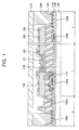
- FIG. 1 is a cross-sectional view of a conventional organic light emitting display
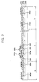
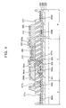
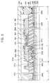
- FIGS. 2 to 5 are cross-sectional views of an organic light emitting display in accordance with embodiments of the invention.
- FIG. 6A is a schematic exploded view of a passive matrix type organic light emitting display device in accordance with one embodiment of the invention.
- FIG. 6B is a schematic exploded view of an active matrix type organic light emitting display device in accordance with one embodiment of the invention.
- FIG. 6C is a schematic top plan view of an organic light emitting display in accordance with one embodiment of the invention.
- FIG. 6D is a cross-sectional view of the organic light emitting display of FIG. 6C, taken along the line d-d.
- FIG. 6E is a schematic perspective view illustrating mass production of organic light emitting devices in accordance with one embodiment of the invention.
- OLED organic light emitting display
- OLED is a display device comprising an array of organic light emitting diodes.
- Organic light emitting diodes are solid state devices which include an organic material and are adapted to generate and emit light when appropriate electrical potentials are applied.
- OLEDs can be generally grouped into two basic types dependent on the arrangement with which the stimulating electrical current is provided.
- Fig. 6A schematically illustrates an exploded view of a simplified structure of a passive matrix type OLED 1000.
- Fig. 6B schematically illustrates a simplified structure of an active matrix type OLED 1001.
- the OLED 1000, 1001 includes OLED pixels built over a substrate 1002, and the OLED pixels include an anode 1004, a cathode 1006 and an organic layer 1010.
- an appropriate electrical current is applied to the anode 1004
- electric current flows through the pixels and visible light is emitted from the organic layer.
- the passive matrix OLED (PMOLED) design includes elongate strips of anode 1004 arranged generally perpendicular to elongate strips of cathode 1006 with organic layers interposed therebetween.
- the intersections of the strips of cathode 1006 and anode 1004 define individual OLED pixels where light is generated and emitted upon appropriate excitation of the corresponding strips of anode 1004 and cathode 1006.
- PMOLEDs provide the advantage of relatively simple fabrication.
- the active matrix OLED includes driving circuits 1012 arranged between the substrate 1002 and an array of OLED pixels.
- An individual pixel of AMOLEDs is defined between the common cathode 1006 and an anode 1004, which is electrically isolated from other anodes.
- Each driving circuit 1012 is coupled with an anode 1004 of the OLED pixels and further coupled with a data line 1016 and a scan line 1018.
- the scan lines 1018 supply scan signals that select rows of the driving circuits
- the data lines 1016 supply data signals for particular driving circuits.
- the data signals and scan signals stimulate the local driving circuits 1012, which excite the anodes 1004 so as to emit light from their corresponding pixels.
- the local driving circuits 1012, the data lines 1016 and scan lines 1018 are buried in a planarization layer 1014, which is interposed between the pixel array and the substrate 1002.
- the planarization layer 1014 provides a planar top surface on which the organic light emitting pixel array is formed.
- the planarization layer 1014 may be formed of organic or inorganic materials, and formed of two or more layers although shown as a single layer.
- the local driving circuits 1012 are typically formed with thin film transistors (TFT) and arranged in a grid or array under the OLED pixel array.
- the local driving circuits 1012 may be at least partly made of organic materials, including organic TFT.
- AMOLEDs have the advantage of fast response time improving their desirability for use in displaying data signals. Also, AMOLEDs have the advantages of consuming less power than passive matrix OLEDs.
- the substrate 1002 provides structural support for the OLED pixels and circuits.
- the substrate 1002 can comprise rigid or flexible materials as well as opaque or transparent materials, such as plastic, glass, and/or foil.
- each OLED pixel or diode is formed with the anode 1004, cathode 1006 and organic layer 1010 interposed therebetween.
- the cathode 1006 injects electrons and the anode 1004 injects holes.
- the anode 1004 and cathode 1006 are inverted; i.e., the cathode is formed on the substrate 1002 and the anode is opposingly arranged.
- Interposed between the cathode 1006 and anode 1004 are one or more organic layers. More specifically, at least one emissive or light emitting layer is interposed between the cathode 1006 and anode 1004.
- the light emitting layer may comprise one or more light emitting organic compounds. Typically, the light emitting layer is configured to emit visible light in a single color such as blue, green, red or white.
- one organic layer 1010 is formed between the cathode 1006 and anode 1004 and acts as a light emitting layer.
- Additional layers, which can be formed between the anode 1004 and cathode 1006, can include a hole transporting layer, a hole injection layer, an electron transporting layer and an electron injection layer.
- Hole transporting and/or injection layers can be interposed between the light emitting layer 1010 and the anode 1004. Electron transporting and/or injecting layers can be interposed between the cathode 1006 and the light emitting layer 1010.
- the electron injection layer facilitates injection of electrons from the cathode 1006 toward the light emitting layer 1010 by reducing the work function for injecting electrons from the cathode 1006.
- the hole injection layer facilitates injection of holes from the anode 1004 toward the light emitting layer 1010.
- the hole and electron transporting layers facilitate movement of the carriers injected from the respective electrodes toward the light emitting layer.
- a single layer may serve both electron injection and transportation functions or both hole injection and transportation functions. In some embodiments, one or more of these layers are lacking. In some embodiments, one or more organic layers are doped with one or more materials that help injection and/or transportation of the carriers. In embodiments where only one organic layer is formed between the cathode and anode, the organic layer may include not only an organic light emitting compound but also certain functional materials that help injection or transportation of carriers within that layer.
- organic materials that have been developed for use in these layers including the light emitting layer. Also, numerous other organic materials for use in these layers are being developed. In some embodiments, these organic materials may be macromolecules including oligomers and polymers. In some embodiments, the organic materials for these layers may be relatively small molecules. The skilled artisan will be able to select appropriate materials for each of these layers in view of the desired functions of the individual layers and the materials for the neighboring layers in particular designs.
- an electrical circuit provides appropriate potential between the cathode 1006 and anode 1004. This results in an electrical current flowing from the anode 1004 to the cathode 1006 via the interposed organic layer(s).
- the cathode 1006 provides electrons to the adjacent organic layer 1010.
- the anode 1004 injects holes to the organic layer 1010.
- the holes and electrons recombine in the organic layer 1010 and generate energy particles called "excitons.”
- the excitons transfer their energy to the organic light emitting material in the organic layer 1010, and the energy is used to emit visible light from the organic light emitting material.
- the spectral characteristics of light generated and emitted by the OLED 1000, 1001 depend on the nature and composition of organic molecules in the organic layer(s).
- the composition of the one or more organic layers can be selected to suit the needs of a particular application by one of ordinary skill in the art.
- OLED devices can also be categorized based on the direction of the light emission. In one type referred to as "top emission” type, OLED devices emit light and display images through the cathode or top electrode 1006. In these embodiments, the cathode 1006 is made of a material transparent or at least partially transparent with respect to visible light. In certain embodiments, to avoid losing any light that can pass through the anode or bottom electrode 1004, the anode may be made of a material substantially reflective of the visible light. A second type of OLED devices emits light through the anode or bottom electrode 1004 and is called “bottom emission” type. In the bottom emission type OLED devices, the anode 1004 is made of a material which is at least partially transparent with respect to visible light.
- the cathode 1006 is made of a material substantially reflective of the visible light.
- a third type of OLED devices emits light in two directions, e.g. through both anode 1004 and cathode 1006.
- the substrate may be formed of a material which is transparent, opaque or reflective of visible light.
- an OLED pixel array 1021 comprising a plurality of organic light emitting pixels is arranged over a substrate 1002 as shown in Fig. 6C.
- the pixels in the array 1021 are controlled to be turned on and off by a driving circuit (not shown), and the plurality of the pixels as a whole displays information or image on the array 1021.
- the OLED pixel array 1021 is arranged with respect to other components, such as drive and control electronics to define a display region and a non-display region.
- the display region refers to the area of the substrate 1002 where OLED pixel array 1021 is formed.
- the non-display region refers to the remaining areas of the substrate 1002.
- the non-display region can contain logic and/or power supply circuitry. It will be understood that there will be at least portions of control/drive circuit elements arranged within the display region. For example, in PMOLEDs, conductive components will extend into the display region to provide appropriate potential to the anode and cathodes. In AMOLEDs, local driving circuits and data/scan lines coupled with the driving circuits will extend into the display region to drive and control the individual pixels of the AMOLEDs.
- FIG. 6D schematically illustrates a cross-section of an encapsulated OLED device 1011 having a layout of Fig. 6C and taken along the line d-d of Fig. 6C.
- a generally planar top plate or substrate 1061 engages with a seal 1071 which further engages with a bottom plate or substrate 1002 to enclose or encapsulate the OLED pixel array 1021.
- one or more layers are formed on the top plate 1061 or bottom plate 1002, and the seal 1071 is coupled with the bottom or top substrate 1002, 1061 via such a layer.
- the seal 1071 extends along the periphery of the OLED pixel array 1021 or the bottom or top plate 1002, 1061.
- the seal 1071 is made of a frit material as will be further discussed below.
- the top and bottom plates 1061, 1002 comprise materials such as plastics, glass and/or metal foils which can provide a barrier to passage of oxygen and/or water to thereby protect the OLED pixel array 1021 from exposure to these substances.
- At least one of the top plate 1061 and the bottom plate 1002 is formed of a substantially transparent material.
- seal 1071 and the top and bottom plates 1061, 1002 provide a substantially non-permeable seal to oxygen and water vapor and provide a substantially hermetically enclosed space 1081.
- the seal 1071 of a frit material in combination with the top and bottom plates 1061, 1002 provide a barrier to oxygen of less than approximately 10 -3 cc/m 2 -day and to water of less than 10 -6 g/m 2 -day.
- a material that can take up oxygen and/or moisture is formed within the enclosed space 1081.
- the seal 1071 has a width W, which is its thickness in a direction parallel to a surface of the top or bottom substrate 1061, 1002 as shown in Fig. 6D.
- the width varies among embodiments and ranges from about 300 ⁇ m to about 3000 ⁇ m, optionally from about 500 ⁇ m to about 1500 ⁇ m. Also, the width may vary at different positions of the seal 1071. In some embodiments, the width of the seal 1071 may be the largest where the seal 1071 contacts one of the bottom and top substrate 1002, 1061 or a layer formed thereon. The width may be the smallest where the seal 1071 contacts the other.
- the width variation in a single cross-section of the seal 1071 relates to the cross-sectional shape of the seal 1071 and other design parameters.
- the seal 1071 has a height H, which is its thickness in a direction perpendicular to a surface of the top or bottom substrate 1061, 1002 as shown in Fig. 6D.
- the height varies among embodiments and ranges from about 2 ⁇ m to about 30 ⁇ m, optionally from about 10 ⁇ m to about 15 ⁇ m. Generally, the height does not significantly vary at different positions of the seal 1071. However, in certain embodiments, the height of the seal 1071 may vary at different positions thereof.
- the seal 1071 has a generally rectangular cross-section. In other embodiments, however, the seal 1071 can have other various cross-sectional shapes such as a generally square cross-section, a generally trapezoidal cross-section, a cross-section with one or more rounded edges, or other configuration as indicated by the needs of a given application. To improve hermeticity, it is generally desired to increase the interfacial area where the seal 1071 directly contacts the bottom or top substrate 1002, 1061 or a layer formed thereon. In some embodiments, the shape of the seal can be designed such that the interfacial area can be increased.
- the seal 1071 can be arranged immediately adjacent the OLED array 1021, and in other embodiments, the seal 1071 is spaced some distance from the OLED array 1021.
- the seal 1071 comprises generally linear segments that are connected together to surround the OLED array 1021. Such linear segments of the seal 1071 can extend, in certain embodiments, generally parallel to respective boundaries of the OLED array 1021. In other embodiment, one or more of the linear segments of the seal 1071 are arranged in a non-parallel relationship with respective boundaries of the OLED array 1021. In yet other embodiments, at least part of the seal 1071 extends between the top plate 1061 and bottom plate 1002 in a curvilinear manner.
- the seal 1071 is formed using a frit material or simply "frit” or “glass frit” which includes fine glass particles.
- the frit particles includes one or more of magnesium oxide (MgO), calcium oxide (CaO), barium oxide (BaO), lithium oxide (Li 2 O), sodium oxide (Na 2 O), potassium oxide (K 2 O), boron oxide (B 2 O 3 ), vanadium oxide (V 2 O 5 ), zinc oxide (ZnO), tellurium oxide (TeO 2 ), aluminum oxide (Al 2 O 3 ), silicon dioxide (SiO 2 ), lead oxide (PbO), tin oxide (SnO), phosphorous oxide (P 2 O 5 ), ruthenium oxide (Ru 2 O), rubidium oxide (Rb 2 O), rhodium oxide (Rh 2 O), ferrite oxide (Fe 2 O 3 ), copper oxide (CuO), titanium oxide (TiO 2 ), tungsten oxide (WO 3 ), bismuth oxide (Bi
- MgO magnesium
- these particles range in size from about 2 ⁇ m to about 30 ⁇ m, optionally about 5 ⁇ m to about 10 ⁇ m, although not limited only thereto.
- the particles can be as large as about the distance between the top and bottom substrates 1061, 1002 or any layers formed on these substrates where the frit seal 1071 contacts.
- the frit material used to form the seal 1071 can also include one or more filler or additive materials.
- the filler or additive materials can be provided to adjust an overall thermal expansion characteristic of the seal 1071 and/or to adjust the absorption characteristics of the seal 1071 for selected frequencies of incident radiant energy.
- the filler or additive material(s) can also include inversion and/or additive fillers to adjust a coefficient of thermal expansion of the frit.
- the filler or additive materials can include transition metals, such as chromium (Cr), iron (Fe), manganese (Mn), cobalt (Co), copper (Cu), and/or vanadium. Additional materials for the filler or additives include ZnSiO 4 , PbTiO 3 , ZrO 2 , eucryptite.
- a frit material as a dry composition contains glass particles from about 20 to 90 about wt%, and the remaining includes fillers and/or additives.
- the frit paste contains about 10-30 wt% organic materials and about 70-90% inorganic materials.
- the frit paste contains about 20 wt% organic materials and about 80 wt% organic materials.
- the organic materials may include about 0-30 wt% binder(s) and about 70-100 wt% solvent(s).
- about 10 wt% is binder(s) and about 90 wt% is solvent(s) among the organic materials.
- the inorganic materials may include about 0-10 wt% additives, about 20-40 wt% fillers and about 50-80 wt% glass powder. In some embodiments, about 0-5 wt% is additive(s), about 25-30 wt% is filler(s) and about 65-75 wt% is the glass powder among the inorganic materials.
- a liquid material is added to the dry frit material to form a frit paste.
- Any organic or inorganic solvent with or without additives can be used as the liquid material.
- the solvent includes one or more organic compounds.
- applicable organic compounds are ethyl cellulose, nitro cellulose, hydroxyl propyl cellulose, butyl carbitol acetate, terpineol, butyl cellusolve, acrylate compounds.
- a shape of the seal 1071 is initially formed from the frit paste and interposed between the top plate 1061 and the bottom plate 1002.
- the seal 1071 can in certain embodiments be pre-cured or pre-sintered to one of the top plate and bottom plate 1061, 1002.
- portions of the seal 1071 are selectively heated such that the frit material forming the seal 1071 at least partially melts.
- the seal 1071 is then allowed to resolidify to form a secure joint between the top plate 1061 and the bottom plate 1002 to thereby inhibit exposure of the enclosed OLED pixel array 1021 to oxygen or water.
- the selective heating of the frit seal is carried out by irradiation of light, such as a laser or directed infrared lamp.
- the frit material forming the seal 1071 can be combined with one or more additives or filler such as species selected for improved absorption of the irradiated light to facilitate heating and melting of the frit material to form the seal 1071.
- OLED devices 1011 are mass produced.
- a plurality of separate OLED arrays 1021 is formed on a common bottom substrate 1101.
- each OLED array 1021 is surrounded by a shaped frit to form the seal 1071.
- common top substrate (not shown) is placed over the common bottom substrate 1101 and the structures formed thereon such that the OLED arrays 1021 and the shaped frit paste are interposed between the common bottom substrate 1101 and the common top substrate.
- the OLED arrays 1021 are encapsulated and sealed, such as via the previously described enclosure process for a single OLED display device.
- the resulting product includes a plurality of OLED devices kept together by the common bottom and top substrates.
- the resulting product is cut into a plurality of pieces, each of which constitutes an OLED device 1011 of Fig. 6D.
- the individual OLED devices 1011 then further undergo additional packaging operations to further improve the sealing formed by the frit seal 1071 and the top and bottom substrates 1061, 1002.
- FIG. 1 is a cross-sectional view of a conventional organic light emitting display.
- the organic light emitting display includes a substrate 100, a semiconductor layer 110, a gate insulating layer 120, a gate electrode 130a, a scan driver 130b, an interlayer insulating layer 140, and source and drain electrodes 150.
- the substrate 100 has a pixel region I and a non-pixel region II.
- the organic light emitting display further includes a common power supply line 150b which is electrically connected to the source and drain electrodes 150.
- the organic light emitting display also includes a second electrode power supply line 150a.
- a planarization layer 160 is disposed over the substantially entire surface of the substrate 100.
- the planarization layer 160 may include an organic material such as acryl-based resin or polyimide-based resin.
- the planarization layer 160 has via-holes for exposing the common power supply line 150b, the second electrode power supply line 150a, and the source and drain electrodes 150.
- the common power supply line 150b is exposed to enhance adhesive strength when the substrate is sealed using a glass frit.
- a first electrode 171 including a reflective layer 170 is disposed over portions of the planarization layer 160 in the pixel region I.
- a pixel defining layer 180 is disposed over the substantially entire surface of the substrate 100.
- An organic layer 190 including at least one emission layer is disposed over the first electrode 171.
- a second electrode 200 is disposed over the organic layer 190.
- An encapsulation substrate 210 is disposed opposite to the substrate 100. The substrate 100 and the encapsulation substrate 210 are sealed with a glass frit 220.
- the illustrated organic light emitting display includes the common power supply line disposed under the glass frit 220 for sealing the substrate.
- the common power supply line has a width wider than the glass frit. Therefore, when a laser beam is radiated to the glass frit, the laser beam may be also radiated to a portion of the common power supply line.
- the common power supply line may transfer a heat generated by the laser to the second power supply line, thereby transferring the heat into an element along the second electrode. This problem may damage the organic layer, degrading the reliability of the organic light emitting display.
- FIGS. 2 to 5 are cross-sectional views of an organic light emitting display in accordance with embodiments of the present invention.
- a substrate 300 includes a pixel region I and a non-pixel region II.
- the substrate 300 may be an insulating glass substrate, a plastic substrate, or a conductive substrate.
- a buffer layer 310 is formed over the substantially entire surface of the substrate 300.
- the buffer layer 310 may be a silicon oxide layer, a silicon nitride layer, or a composite layer of silicon oxide and silicon nitride.
- the buffer layer 310 may functions as a passivation layer for preventing impurities from out-diffusing from the substrate 300.
- a semiconductor layer 320 is formed on a portion of the buffer layer 310 in the pixel region I.
- the semiconductor layer 320 may include amorphous silicon or polysilicon.
- a gate insulating layer 330 is formed over the substantially entire surface of the substrate 300.
- the gate insulating layer 330 may be a silicon oxide layer, a silicon nitride layer, or a composite layer of silicon oxide and silicon nitride.
- a gate electrode 340a is formed over the gate insulating layer 330.
- the gate electrode 340a overlaps with a portion of the semiconductor layer 320.
- the gate electrode 340a may be formed of Al, Cu, or Cr.
- an interlayer insulating layer 350 is formed over the substantially entire surface of the substrate 300.
- the interlayer insulating layer 350 may be a silicon oxide layer, a silicon nitride layer, or a composite layer of silicon oxide and silicon nitride.
- the interlayer insulating layer 350 and the gate insulating layer 330 in the pixel region I are etched to form contact holes 351 and 352 for exposing portions of the semiconductor layer 320.
- source and drain electrodes 360a and 360b are formed on the interlayer insulating layer 350 in the pixel region I.
- the source and drain electrodes 360a and 360b may be formed of one selected from the group consisting of Mo, Cr, Al, Ti, Au, Pd and Ag.
- the source and drain electrodes 360a and 360b are electrically connected to the semiconductor layer 320 through the contact holes 351 and 352.
- a conductive line 360d may be formed in the non-pixel region II.
- the conductive line 360d may act as a common power supply line.
- a second electrode power supply line 360c may also be formed at the same time.
- a scan driver 340b may be formed in the non-pixel region II.
- the conductive line 360d in the non-pixel region II is narrower than a glass frit 430 ( Figure 5) which will be formed over the conductive line 360d.
- the glass frit 430 may have a portion overlapping the conductive line 360d. When viewed from above (i.e. in a direction perpendicular to the substrate 300), the portion of the glass frit substantially eclipses the conductive line 360d.
- the glass frit may have a width W1 between about 0.6mm and about 0.7mm. The width W1 of the glass frit, however, may vary depending on the design of an OLED device.
- the width W2 of the conductive line 360d may be adapted to that of the glass frit.
- the width W2 of the conductive line 360d is about 10%, about 20%, about 30%, about 40%, about 50%, about 60%, about 65%, about 70%, about 75%, about 80%, about 85%, about 90%, about 95%, about 96%, about 97%, about 98%, about 99%, or about 100% of the maximum width W1 of the glass frit 430.
- the glass frit serves as a sealant for the OLED device, as will be described later in more detail.
- the glass frit is attached to at least a portion of the top surface of the conductive line 360d by a laser process.
- a laser beam is irradiated onto the glass frit from above.
- the diameter of the laser beam may be equal to or larger than the width of the glass frit.
- At least a portion of the laser beam may be irradiated on edge portions of the glass frit.
- the diameter of the laser beam may be smaller than the width of the glass frit.
- the laser beam may be irradiated onto the edge portions of the glass frit by moving the laser beam over the edge portions.
- the conductive line may be exposed to the laser beam during the laser process.
- the conductive line may transfer a heat generated by the laser beam to the second electrode power supply line.
- the heat may be transferred through the second electrode to another element.
- This problem causes damages to an organic layer in the pixel region I.
- the illustrated conductive line 360d has a narrower width than that of the glass frit sealant.
- the substantially entire portion of the conductive line 360d is covered by the glass frit. This configuration prevents the conductive line 360d from being exposed to the laser beam during the laser process.
- a top-gate thin film transistor is described.
- the conductive line structure may apply to a bottom-gate thin film transistor having a gate electrode disposed under a semiconductor layer.
- the conductive line may be formed simultaneously with forming the gate electrode or a first electrode which will be described later.
- a planarization layer 370 is formed over the substantially entire surface of the substrate 300.
- the planarization layer 370 may include an organic layer, an inorganic layer, or a composite layer thereof.
- the inorganic layer may be formed by spin on glass (SOG).
- the organic layer may include an acryl-based resin, a polyimide-based resin, or benzocyclobutene (BCB).
- the planarization layer 370 in the pixel region I is etched to form a via-hole 371a for exposing one of the source and drain electrodes.
- the planarization layer 370 in the non-pixel region II is etched to form openings 371b and 371c for exposing the conductive line 360d and the second electrode power supply line 360c.
- the conductive line 360d is exposed to increase adhesive strength with the substrate when the substrate is sealed by the glass frit.
- a first electrode 380 including a reflective layer 375 is formed on the planarization 370 in the pixel region I.
- the first electrode 380 is disposed on a bottom surface of the via-hole 371 to be in contact with one of the exposed source and drain electrodes 360a and 360b.
- the first electrode 380 also extends onto portions of the planarization layer 370.
- the first electrode 380 may be formed of indium tin oxide (ITO) or indium zinc oxide (IZO).
- a pixel defining layer 390 is formed over the substantially entire surface of the substrate 300.
- the pixel defining layer 390 also covers the first electrode 380 to a thickness sufficient to fill the via-hole 371a, in which the first electrode 380 is disposed.
- the pixel defining layer 390 may be formed of an organic layer or an inorganic layer.
- the pixel defining layer 390 is formed of one selected from the group consisting of BCB, an acryl-based polymer, and polyimide.
- the pixel defining layer 390 may have high flowability such that the pixel defining layer can be evenly formed over the substantially entire surface of the substrate.
- the pixel defining layer 390 is etched to form an opening 395a for exposing the first electrode 380 in the pixel region I, and an opening 395b for exposing a portion of the second electrode power supply line 360c in the non-pixel region II.
- the pixel defining layer 390 is also etched to expose a portion of the conductive line 360d in the non-pixel region II.
- an organic layer 400 is formed on the first electrode 380 exposed through the opening 395a.
- the organic layer 400 includes at least an emission layer.
- the organic layer 400 may further include at least one of a hole injection layer, a hole transport layer, an electron transport layer, and an electron injection layer.
- a second electrode 410 is formed over the substantially entire surface of the substrate 300.
- the second electrode 410 is a transmissive electrode.
- the second electrode may be formed of Mg, Ag, Al, Ca, or an alloy of two or more of the foregoing.
- the second electrode may be formed of a material which is transparent and has a low work function.
- the second electrode 410 in the non-pixel region II may be etched to expose the conductive line 360d and the planarization layer 370.
- an encapsulation substrate 420 is placed opposite to the substrate 300.
- the encapsulation substrate 420 may be formed of an etched insulating glass or a non-etched insulating glass.
- the glass frit 430 may be formed of one or more materials selected from the group consisting of magnesium oxide (MgO), calcium oxide (CaO), barium oxide (BaO), lithium oxide (Li 2 O), sodium oxide (Na 2 O), potassium oxide (K 2 O), boron oxide (B 2 O 3 ), vanadium oxide (V 2 O 5 ), zinc oxide (ZnO), tellurium oxide (TeO 2 ), aluminum oxide (Al 2 O 3 ), silicon dioxide (SiO 2 ), lead oxide (PbO), tin oxide (SnO), phosphorous oxide (P 2 O 5 ), ruthenium oxide (Ru 2 O), rubidium oxide (Rb 2 O), rhodium oxide (Rh 2 O), ferrite oxide (Fe 2 O 3 ), copper oxide (CuO), titanium oxide (TiO 2 ) tungsten oxide (WO 3 ), bismuth oxide (Bi 2 O 3 ), copper oxide (CuO), titanium oxide (TiO 2 ) tungsten oxide (WO 3
- the glass frit 430 is first applied to the encapsulation substrate 420 and then the encapsulation substrate 420 with the glass frit 430 is placed over the substrate 300.
- the glass frit 430 may be first applied to the substrate 300, and then the encapsulation substrate 420 is placed over the substrate 300.
- the encapsulation substrate 420 is aligned with the substrate 300.
- the glass frit 430 is in contact with the conductive line 360d and the planarization layer 370 formed over the substrate 300.
- the glass frit 430 is irradiated with a laser beam, the glass frit 430 is melted and solidified to adhere to the substrate and the encapsulation substrate, thereby sealing the organic light emitting display.
- the illustrated conductive line has a width narrower than that of the glass frit, thereby reducing heat transfer to elements in the pixel region during the laser process.
- the reliability of the resulting OLED can be improved.
Landscapes
- Health & Medical Sciences (AREA)
- Engineering & Computer Science (AREA)
- Life Sciences & Earth Sciences (AREA)
- Animal Behavior & Ethology (AREA)
- Anesthesiology (AREA)
- Biomedical Technology (AREA)
- Heart & Thoracic Surgery (AREA)
- Hematology (AREA)
- Veterinary Medicine (AREA)
- Vascular Medicine (AREA)
- General Health & Medical Sciences (AREA)
- Public Health (AREA)
- Environmental & Geological Engineering (AREA)
- Physics & Mathematics (AREA)
- Optics & Photonics (AREA)
- Electroluminescent Light Sources (AREA)
- Devices For Indicating Variable Information By Combining Individual Elements (AREA)
Applications Claiming Priority (1)
| Application Number | Priority Date | Filing Date | Title |
|---|---|---|---|
| KR1020060007025A KR100635514B1 (ko) | 2006-01-23 | 2006-01-23 | 유기전계발광표시장치 및 그 제조방법 |
Publications (3)
| Publication Number | Publication Date |
|---|---|
| EP1811571A2 true EP1811571A2 (de) | 2007-07-25 |
| EP1811571A3 EP1811571A3 (de) | 2011-02-02 |
| EP1811571B1 EP1811571B1 (de) | 2019-01-16 |
Family
ID=37626512
Family Applications (1)
| Application Number | Title | Priority Date | Filing Date |
|---|---|---|---|
| EP07250270.1A Active EP1811571B1 (de) | 2006-01-23 | 2007-01-23 | Organische lichtemittierende Anzeigevorrichtung und Herstellungsverfahren |
Country Status (6)
| Country | Link |
|---|---|
| US (1) | US8120249B2 (de) |
| EP (1) | EP1811571B1 (de) |
| JP (1) | JP4472668B2 (de) |
| KR (1) | KR100635514B1 (de) |
| CN (1) | CN101009311B (de) |
| TW (1) | TWI341144B (de) |
Cited By (7)
| Publication number | Priority date | Publication date | Assignee | Title |
|---|---|---|---|---|
| US7992411B2 (en) | 2008-05-30 | 2011-08-09 | Corning Incorporated | Method for sintering a frit to a glass plate |
| US8147632B2 (en) | 2008-05-30 | 2012-04-03 | Corning Incorporated | Controlled atmosphere when sintering a frit to a glass plate |
| WO2016155354A1 (en) | 2015-03-30 | 2016-10-06 | Boe Technology Group Co., Ltd. | Oled touch-control substrate and fabrication method thereof, and display apparatus |
| US9761827B2 (en) | 2011-11-29 | 2017-09-12 | Semiconductor Energy Laboratory Co., Ltd. | Sealed structure, light-emitting device, electronic device, and lighting device |
| US10068926B2 (en) | 2011-05-05 | 2018-09-04 | Semiconductor Energy Laboratory Co., Ltd. | Semiconductor device and method for manufacturing the same |
| CN113387601A (zh) * | 2021-05-31 | 2021-09-14 | 西南电子技术研究所(中国电子科技集团公司第十研究所) | 高真空磁控溅射界面辅助提高玻璃焊接强度的方法 |
| US11362302B2 (en) * | 2017-08-09 | 2022-06-14 | Kunshan Go-Visionox Opto-Electronics Co., Ltd. | Array substrate, manufacturing method thereof and display panel |
Families Citing this family (75)
| Publication number | Priority date | Publication date | Assignee | Title |
|---|---|---|---|---|
| US7928654B2 (en) * | 2003-08-29 | 2011-04-19 | Semiconductor Energy Laboratory Co., Ltd. | Display device and method for manufacturing the same |
| US20070108900A1 (en) * | 2005-11-15 | 2007-05-17 | Boek Heather D | Method and apparatus for the elimination of interference fringes in an OLED device |
| US7537504B2 (en) * | 2005-12-06 | 2009-05-26 | Corning Incorporated | Method of encapsulating a display element with frit wall and laser beam |
| US7425166B2 (en) * | 2005-12-06 | 2008-09-16 | Corning Incorporated | Method of sealing glass substrates |
| US7597603B2 (en) * | 2005-12-06 | 2009-10-06 | Corning Incorporated | Method of encapsulating a display element |
| US8038495B2 (en) | 2006-01-20 | 2011-10-18 | Samsung Mobile Display Co., Ltd. | Organic light-emitting display device and manufacturing method of the same |
| KR100673765B1 (ko) | 2006-01-20 | 2007-01-24 | 삼성에스디아이 주식회사 | 유기전계발광 표시장치 및 그 제조방법 |
| JP4624309B2 (ja) * | 2006-01-24 | 2011-02-02 | 三星モバイルディスプレイ株式會社 | 有機電界発光表示装置及びその製造方法 |
| JP4456092B2 (ja) * | 2006-01-24 | 2010-04-28 | 三星モバイルディスプレイ株式會社 | 有機電界発光表示装置及びその製造方法 |
| US8164257B2 (en) * | 2006-01-25 | 2012-04-24 | Samsung Mobile Display Co., Ltd. | Organic light emitting display and method of fabricating the same |
| KR100688795B1 (ko) * | 2006-01-25 | 2007-03-02 | 삼성에스디아이 주식회사 | 유기전계발광 표시장치 및 그 제조방법 |
| KR100685853B1 (ko) * | 2006-01-25 | 2007-02-22 | 삼성에스디아이 주식회사 | 유기전계발광표시장치 및 그 제조방법 |
| KR100671641B1 (ko) | 2006-01-25 | 2007-01-19 | 삼성에스디아이 주식회사 | 유기 전계 발광 표시장치 및 그 제조 방법 |
| KR100688796B1 (ko) * | 2006-01-25 | 2007-03-02 | 삼성에스디아이 주식회사 | 유기전계발광 표시 장치 및 그의 제작 방법 |
| KR100732808B1 (ko) * | 2006-01-26 | 2007-06-27 | 삼성에스디아이 주식회사 | 유기전계발광 표시장치의 제조방법 |
| KR100671647B1 (ko) * | 2006-01-26 | 2007-01-19 | 삼성에스디아이 주식회사 | 유기전계발광 표시 장치 |
| JP4633674B2 (ja) | 2006-01-26 | 2011-02-16 | 三星モバイルディスプレイ株式會社 | 有機電界発光表示装置及びその製造方法 |
| KR100688792B1 (ko) * | 2006-01-27 | 2007-03-02 | 삼성에스디아이 주식회사 | 평판 표시장치 및 그의 제조방법 |
| KR100688790B1 (ko) * | 2006-01-27 | 2007-03-02 | 삼성에스디아이 주식회사 | 유기 전계 발광 표시장치 및 그 제조 방법 |
| KR100759666B1 (ko) * | 2006-01-27 | 2007-09-17 | 삼성에스디아이 주식회사 | 평판 표시장치 및 그의 제조방법 |
| KR100671639B1 (ko) * | 2006-01-27 | 2007-01-19 | 삼성에스디아이 주식회사 | 유기 전계 발광 표시장치 및 그 제조 방법 |
| US20070188757A1 (en) * | 2006-02-14 | 2007-08-16 | Jeffrey Michael Amsden | Method of sealing a glass envelope |
| KR100732817B1 (ko) | 2006-03-29 | 2007-06-27 | 삼성에스디아이 주식회사 | 유기전계발광 표시장치 및 그 제조방법 |
| US20070267972A1 (en) * | 2006-05-22 | 2007-11-22 | Menegus Harry E | Method for forming a temporary hermetic seal for an OLED display device |
| US20080124558A1 (en) * | 2006-08-18 | 2008-05-29 | Heather Debra Boek | Boro-silicate glass frits for hermetic sealing of light emitting device displays |
| US20080048556A1 (en) * | 2006-08-24 | 2008-02-28 | Stephan Lvovich Logunov | Method for hermetically sealing an OLED display |
| US20080049431A1 (en) * | 2006-08-24 | 2008-02-28 | Heather Debra Boek | Light emitting device including anti-reflection layer(s) |
| US7800303B2 (en) * | 2006-11-07 | 2010-09-21 | Corning Incorporated | Seal for light emitting display device, method, and apparatus |
| US20080168801A1 (en) * | 2007-01-12 | 2008-07-17 | Paul Stephen Danielson | Method of sealing glass |
| US20080200088A1 (en) * | 2007-02-21 | 2008-08-21 | Chong Pyung An | Method for reducing interference fringes in a display device |
| US7652305B2 (en) * | 2007-02-23 | 2010-01-26 | Corning Incorporated | Methods and apparatus to improve frit-sealed glass package |
| US20080213482A1 (en) * | 2007-03-01 | 2008-09-04 | Stephan Lvovich Logunov | Method of making a mask for sealing a glass package |
| KR100858617B1 (ko) | 2007-05-10 | 2008-09-17 | 삼성에스디아이 주식회사 | 박막 트랜지스터 및 이를 이용한 유기 전계 발광표시장치 |
| KR100846968B1 (ko) | 2007-05-21 | 2008-07-17 | 삼성에스디아이 주식회사 | 유기전계발광표시장치 |
| US20090044496A1 (en) * | 2007-08-16 | 2009-02-19 | Botelho John W | Method and apparatus for sealing a glass package |
| KR100922063B1 (ko) | 2008-02-04 | 2009-10-16 | 삼성모바일디스플레이주식회사 | 유기 전계 발광표시장치 |
| US8448468B2 (en) | 2008-06-11 | 2013-05-28 | Corning Incorporated | Mask and method for sealing a glass envelope |
| US20100095705A1 (en) | 2008-10-20 | 2010-04-22 | Burkhalter Robert S | Method for forming a dry glass-based frit |
| KR101002659B1 (ko) * | 2008-12-23 | 2010-12-20 | 삼성모바일디스플레이주식회사 | 유기 발광 표시 장치 |
| JP5240718B2 (ja) * | 2009-02-20 | 2013-07-17 | パナソニック株式会社 | 有機elモジュール |
| KR101084230B1 (ko) * | 2009-11-16 | 2011-11-16 | 삼성모바일디스플레이주식회사 | 유기 발광 표시 장치 및 유기 발광 표시 장치의 제조 방법 |
| KR101626840B1 (ko) | 2010-03-05 | 2016-06-02 | 야마토 덴시 가부시키가이샤 | 유기 el 봉착용 무연 유리재와 이것을 사용한 유기 el 디스플레이 |
| CN101847652B (zh) * | 2010-04-21 | 2011-08-17 | 友达光电股份有限公司 | 电致发光显示面板 |
| KR101234228B1 (ko) * | 2010-06-04 | 2013-02-18 | 삼성디스플레이 주식회사 | 유기 발광 표시 장치 |
| KR101827551B1 (ko) * | 2010-10-15 | 2018-03-23 | 삼성디스플레이 주식회사 | 유기 발광 표시 장치 및 그 제조 방법 |
| WO2013031509A1 (en) * | 2011-08-26 | 2013-03-07 | Semiconductor Energy Laboratory Co., Ltd. | Light-emitting device, electronic device, lighting device, and method for manufacturing the light-emitting device |
| CN102709480B (zh) * | 2011-11-25 | 2016-01-27 | 京东方科技集团股份有限公司 | 有机电致发光器件及显示器 |
| KR102058387B1 (ko) * | 2011-11-28 | 2019-12-24 | 가부시키가이샤 한도오따이 에네루기 켄큐쇼 | 유리 패턴 및 그 형성 방법, 밀봉체 및 그 제작 방법, 및 발광 장치 |
| KR102001815B1 (ko) | 2011-11-29 | 2019-07-19 | 가부시키가이샤 한도오따이 에네루기 켄큐쇼 | 밀봉체의 제작 방법 및 발광 장치의 제작 방법 |
| KR20140016170A (ko) * | 2012-07-30 | 2014-02-07 | 가부시키가이샤 한도오따이 에네루기 켄큐쇼 | 밀봉체 및 유기 전계 발광 장치 |
| EP2890653B1 (de) | 2012-08-30 | 2016-08-24 | Corning Incorporated | Antimonfreies glas, antimonfreie glasmasse und mit der glasmasse luftdicht versiegeltes glasgehäuse |
| DE102012109258B4 (de) * | 2012-09-28 | 2020-02-06 | Osram Oled Gmbh | Optoelektronisches Bauelement und Verfahren zum Herstellen eines optoelektronischen Bauelementes |
| KR101993331B1 (ko) * | 2013-01-03 | 2019-06-27 | 삼성디스플레이 주식회사 | 유기발광표시장치 및 그 제조방법 |
| CN103943649B (zh) * | 2013-02-15 | 2017-10-03 | 上海天马微电子有限公司 | Oled显示面板及其驱动方法 |
| KR20150043136A (ko) | 2013-10-14 | 2015-04-22 | 삼성디스플레이 주식회사 | 유기 발광 표시 장치 및 이의 제조 방법 |
| KR102207563B1 (ko) * | 2013-10-29 | 2021-01-27 | 삼성디스플레이 주식회사 | 유기 발광 표시장치 및 유기 발광 표시장치의 제조 방법 |
| KR20150071318A (ko) * | 2013-12-18 | 2015-06-26 | 삼성디스플레이 주식회사 | 유기 발광 표시 장치의 제조 방법 |
| KR102223676B1 (ko) | 2014-06-24 | 2021-03-08 | 삼성디스플레이 주식회사 | 디스플레이 장치 |
| KR102360783B1 (ko) | 2014-09-16 | 2022-02-10 | 삼성디스플레이 주식회사 | 디스플레이 장치 |
| CN104538566A (zh) * | 2015-01-22 | 2015-04-22 | 深圳市华星光电技术有限公司 | Oled的封装方法及oled封装结构 |
| CN104617007B (zh) * | 2015-01-23 | 2017-08-01 | 京东方科技集团股份有限公司 | 提高封装胶图形密封性测试准确性的方法、母板和掩膜板 |
| KR102483950B1 (ko) * | 2015-04-28 | 2023-01-03 | 삼성디스플레이 주식회사 | 디스플레이 장치 실링용 조성물, 이를 포함한 유기발광 디스플레이 장치 및 그 제조방법 |
| KR102451728B1 (ko) * | 2015-05-19 | 2022-10-07 | 삼성디스플레이 주식회사 | 유기발광 디스플레이 장치 및 그 제조방법 |
| CN105739154B (zh) * | 2016-04-29 | 2019-09-27 | 上海天马有机发光显示技术有限公司 | 一种显示面板以及电子设备 |
| KR102610710B1 (ko) * | 2016-06-10 | 2023-12-08 | 삼성디스플레이 주식회사 | 표시 장치 및 그의 제조방법 |
| CN107046104A (zh) * | 2017-01-10 | 2017-08-15 | 广东欧珀移动通信有限公司 | Oled封装结构及其制备方法 |
| KR102481863B1 (ko) * | 2017-09-15 | 2022-12-26 | 엘지디스플레이 주식회사 | 표시 장치 |
| CN111758300B (zh) * | 2018-02-26 | 2023-08-29 | 夏普株式会社 | 显示装置以及其制造方法 |
| KR102663522B1 (ko) | 2018-11-05 | 2024-05-16 | 삼성디스플레이 주식회사 | 표시장치 및 그 제조방법 |
| CN109728195B (zh) * | 2018-12-29 | 2021-05-18 | 厦门天马微电子有限公司 | 显示面板以及显示装置 |
| KR102763278B1 (ko) * | 2019-12-31 | 2025-02-10 | 삼성디스플레이 주식회사 | 표시 패널 |
| TWI729862B (zh) * | 2020-06-22 | 2021-06-01 | 友達光電股份有限公司 | 有機發光面板及其製作方法 |
| CN111732342B (zh) * | 2020-08-07 | 2022-12-27 | 上海银浆科技有限公司 | 一种玻璃组分以及含有所述的玻璃组分的晶硅太阳能电池导电银浆 |
| KR102886548B1 (ko) | 2020-10-29 | 2025-11-14 | 삼성디스플레이 주식회사 | 표시 장치 |
| CN116018897A (zh) * | 2021-08-19 | 2023-04-25 | 京东方科技集团股份有限公司 | 显示装置、显示面板及其制造方法 |
Citations (3)
| Publication number | Priority date | Publication date | Assignee | Title |
|---|---|---|---|---|
| JPH1074583A (ja) | 1996-08-30 | 1998-03-17 | Sanyo Electric Co Ltd | 有機elディスプレイ及び有機elディスプレイの 製造方法 |
| US20040207314A1 (en) | 2003-04-16 | 2004-10-21 | Aitken Bruce G. | Glass package that is hermetically sealed with a frit and method of fabrication |
| CN1625309A (zh) | 2004-07-09 | 2005-06-08 | 友达光电股份有限公司 | 显示装置 |
Family Cites Families (178)
| Publication number | Priority date | Publication date | Assignee | Title |
|---|---|---|---|---|
| US3966449A (en) | 1975-02-10 | 1976-06-29 | International Business Machines Corporation | Sealing glass composition and process |
| US4105292A (en) | 1975-09-02 | 1978-08-08 | Minnesota Mining And Manufacturing Company | Optical element to assure a minimum spacing |
| US4004936A (en) | 1976-05-19 | 1977-01-25 | International Business Machines Corporation | Low temperature sealed glass compositions and process for their preparation |
| US4238704A (en) | 1979-02-12 | 1980-12-09 | Corning Glass Works | Sealed beam lamp of borosilicate glass with a sealing glass of zinc silicoborate and a mill addition of cordierite |
| JPS5966157A (ja) | 1982-10-08 | 1984-04-14 | Fujitsu Ltd | 半導体装置及びその製造方法 |
| JPS60216333A (ja) | 1984-04-12 | 1985-10-29 | Asahi Glass Co Ltd | エレクトロクロミツク表示素子 |
| JPH0682765B2 (ja) | 1985-12-25 | 1994-10-19 | 株式会社日立製作所 | 液晶表示素子 |
| US6980275B1 (en) | 1993-09-20 | 2005-12-27 | Semiconductor Energy Laboratory Co., Ltd. | Electro-optical device |
| JP3135793B2 (ja) | 1994-09-02 | 2001-02-19 | シャープ株式会社 | 液晶表示装置およびその製造方法 |
| US6195142B1 (en) | 1995-12-28 | 2001-02-27 | Matsushita Electrical Industrial Company, Ltd. | Organic electroluminescence element, its manufacturing method, and display device using organic electroluminescence element |
| US5811927A (en) | 1996-06-21 | 1998-09-22 | Motorola, Inc. | Method for affixing spacers within a flat panel display |
| US6109994A (en) | 1996-12-12 | 2000-08-29 | Candescent Technologies Corporation | Gap jumping to seal structure, typically using combination of vacuum and non-vacuum environments |
| JPH10270592A (ja) | 1997-03-24 | 1998-10-09 | Texas Instr Japan Ltd | 半導体装置及びその製造方法 |
| JP3169864B2 (ja) | 1997-09-18 | 2001-05-28 | 日本電気株式会社 | 液晶パネル製造装置 |
| US5965907A (en) | 1997-09-29 | 1999-10-12 | Motorola, Inc. | Full color organic light emitting backlight device for liquid crystal display applications |
| JP3024609B2 (ja) | 1997-10-09 | 2000-03-21 | 日本電気株式会社 | 液晶表示素子セルの封孔装置 |
| JP2845239B1 (ja) | 1997-12-17 | 1999-01-13 | 日本電気株式会社 | 有機薄膜elデバイスおよびその製造方法 |
| JPH11329717A (ja) | 1998-05-15 | 1999-11-30 | Sharp Corp | カラーelパネル |
| JP3912711B2 (ja) | 1998-11-27 | 2007-05-09 | ローム株式会社 | 有機el素子 |
| JP3517624B2 (ja) | 1999-03-05 | 2004-04-12 | キヤノン株式会社 | 画像形成装置 |
| JP2000268969A (ja) | 1999-03-17 | 2000-09-29 | Tdk Corp | 有機el素子 |
| JP2000306664A (ja) | 1999-04-21 | 2000-11-02 | Stanley Electric Co Ltd | 有機el表示装置 |
| TWI240592B (en) | 1999-06-03 | 2005-09-21 | Koninkl Philips Electronics Nv | Organic electroluminescent device |
| JP2001022293A (ja) | 1999-07-07 | 2001-01-26 | Sony Corp | 平面表示素子 |
| JP2001052858A (ja) | 1999-08-05 | 2001-02-23 | Futaba Corp | 有機el表示装置 |
| US6452323B1 (en) | 1999-09-20 | 2002-09-17 | Omnion Technologies, Inc. | Luminous gas discharge display having dielectric sealing layer |
| JP3942770B2 (ja) | 1999-09-22 | 2007-07-11 | 株式会社半導体エネルギー研究所 | El表示装置及び電子装置 |
| JP4345153B2 (ja) | 1999-09-27 | 2009-10-14 | ソニー株式会社 | 映像表示装置の製造方法 |
| JP3423261B2 (ja) | 1999-09-29 | 2003-07-07 | 三洋電機株式会社 | 表示装置 |
| US6833668B1 (en) | 1999-09-29 | 2004-12-21 | Sanyo Electric Co., Ltd. | Electroluminescence display device having a desiccant |
| JP2001110564A (ja) | 1999-10-07 | 2001-04-20 | Gunze Ltd | エレクトロルミネッセンスランプ |
| KR100480146B1 (ko) | 1999-10-30 | 2005-04-06 | 엘지.필립스 엘시디 주식회사 | 액정표시소자의 제조장치 및 방법 |
| KR100720066B1 (ko) | 1999-11-09 | 2007-05-18 | 가부시키가이샤 한도오따이 에네루기 켄큐쇼 | 발광장치 제작방법 |
| WO2002021557A1 (en) | 2000-09-06 | 2002-03-14 | Osram Opto Semiconductors Gmbh | Encapsulation for oled devices |
| JP3409764B2 (ja) | 1999-12-28 | 2003-05-26 | 日本電気株式会社 | 有機el表示パネルの製造方法 |
| US6515417B1 (en) | 2000-01-27 | 2003-02-04 | General Electric Company | Organic light emitting device and method for mounting |
| US6555025B1 (en) | 2000-01-31 | 2003-04-29 | Candescent Technologies Corporation | Tuned sealing material for sealing of a flat panel display |
| US6624572B1 (en) | 2000-02-17 | 2003-09-23 | Lg Electronics, Inc. | Organic electroluminescence display panel and method for sealing the same |
| JP2001230072A (ja) | 2000-02-18 | 2001-08-24 | Denso Corp | 有機el表示装置 |
| US6650392B2 (en) | 2000-03-15 | 2003-11-18 | Kabushiki Kaisha Toshiba | Cell structure of liquid crystal device |
| JP2001307633A (ja) | 2000-04-20 | 2001-11-02 | Mitsubishi Electric Corp | フラットディスプレイパネル、フラットディスプレイ装置およびフラットディスプレイパネルの製造方法 |
| US7579203B2 (en) | 2000-04-25 | 2009-08-25 | Semiconductor Energy Laboratory Co., Ltd. | Light emitting device |
| JP2001319775A (ja) | 2000-05-10 | 2001-11-16 | Auto Network Gijutsu Kenkyusho:Kk | 有機el表示装置の封止方法および封止構造 |
| JP2001324662A (ja) | 2000-05-16 | 2001-11-22 | Ricoh Co Ltd | レンズ連動機構 |
| JP2002020169A (ja) | 2000-07-03 | 2002-01-23 | Murata Mfg Co Ltd | 高周波用誘電体磁器組成物、誘電体共振器、誘電体フィルタ、誘電体デュプレクサおよび通信機装置 |
| JP4889883B2 (ja) | 2000-07-10 | 2012-03-07 | 株式会社半導体エネルギー研究所 | 成膜方法および成膜装置 |
| US6956324B2 (en) | 2000-08-04 | 2005-10-18 | Semiconductor Energy Laboratory Co., Ltd. | Semiconductor device and manufacturing method therefor |
| US6605826B2 (en) | 2000-08-18 | 2003-08-12 | Semiconductor Energy Laboratory Co., Ltd. | Light-emitting device and display device |
| JP2002169135A (ja) | 2000-09-07 | 2002-06-14 | Seiko Epson Corp | セルギャップ調整装置、加圧封止装置及び液晶表示装置の製造方法 |
| JP4801297B2 (ja) | 2000-09-08 | 2011-10-26 | 株式会社半導体エネルギー研究所 | 発光装置 |
| US6924594B2 (en) | 2000-10-03 | 2005-08-02 | Semiconductor Energy Laboratory Co., Ltd. | Light emitting device |
| JP2002117777A (ja) | 2000-10-11 | 2002-04-19 | Matsushita Electric Ind Co Ltd | ガス放電パネルおよびガス放電パネルの製造方法 |
| US7178927B2 (en) | 2000-11-14 | 2007-02-20 | Semiconductor Energy Laboratory Co., Ltd. | Electroluminescent device having drying agent |
| JP4223211B2 (ja) | 2000-11-14 | 2009-02-12 | 株式会社半導体エネルギー研究所 | 発光装置の作製方法 |
| JP2002170664A (ja) | 2000-12-05 | 2002-06-14 | Toray Ind Inc | 有機電界発光素子 |
| US6646284B2 (en) | 2000-12-12 | 2003-11-11 | Semiconductor Energy Laboratory Co., Ltd. | Light emitting device and method of manufacturing the same |
| MY145695A (en) | 2001-01-24 | 2012-03-30 | Nichia Corp | Light emitting diode, optical semiconductor device, epoxy resin composition suited for optical semiconductor device, and method for manufacturing the same |
| US6554672B2 (en) | 2001-03-12 | 2003-04-29 | Micron Technology, Inc. | Flat panel display, method of high vacuum sealing |
| JP2002280169A (ja) | 2001-03-19 | 2002-09-27 | Futaba Corp | 有機el装置 |
| TWI222838B (en) | 2001-04-10 | 2004-10-21 | Chi Mei Optoelectronics Corp | Packaging method of organic electroluminescence light-emitting display device |
| JP2002318547A (ja) | 2001-04-24 | 2002-10-31 | Sony Corp | 表示パネルの製造方法 |
| US6424009B1 (en) | 2001-05-04 | 2002-07-23 | Advanced Micro Devices, Inc. | Polysilicon insulator material in semiconductor-on-insulator (SOI) structure |
| JP2005510831A (ja) | 2001-05-24 | 2005-04-21 | オリオン エレクトリック カンパニー,リミテッド | 有機発光ダイオードのエンカプセレーションのための容器及びその製造方法 |
| JP2002359070A (ja) | 2001-05-31 | 2002-12-13 | Matsushita Electric Ind Co Ltd | 有機発光素子およびそれを用いた表示パネル |
| US6565400B1 (en) | 2001-06-26 | 2003-05-20 | Candescent Technologies Corporation | Frit protection in sealing process for flat panel displays |
| US6660547B2 (en) | 2001-07-26 | 2003-12-09 | Osram Opto Semiconductors Gmbh | Stabilization for thin substrates |
| JP2003068472A (ja) | 2001-08-29 | 2003-03-07 | Hitachi Ltd | 有機発光素子およびそれを用いた有機発光表示装置 |
| TW517356B (en) | 2001-10-09 | 2003-01-11 | Delta Optoelectronics Inc | Package structure of display device and its packaging method |
| US20030077396A1 (en) | 2001-10-23 | 2003-04-24 | Lecompte Robert S. | Dip coating system |
| KR100865284B1 (ko) | 2001-10-31 | 2008-10-27 | 엘지디스플레이 주식회사 | 액정패널의 실링구조 |
| TW564563B (en) | 2001-11-29 | 2003-12-01 | Highlink Technology Corp | Light-emitting device with increased stability |
| KR100819864B1 (ko) | 2001-12-28 | 2008-04-07 | 엘지.필립스 엘시디 주식회사 | 유기전기발광소자 |
| TW515062B (en) | 2001-12-28 | 2002-12-21 | Delta Optoelectronics Inc | Package structure with multiple glue layers |
| US7038377B2 (en) | 2002-01-16 | 2006-05-02 | Seiko Epson Corporation | Display device with a narrow frame |
| CN1212662C (zh) | 2002-01-16 | 2005-07-27 | 翰立光电股份有限公司 | 显示元件的封装构造 |
| JP2003216059A (ja) | 2002-01-24 | 2003-07-30 | Sharp Corp | 表示素子およびその製造方法 |
| JP2003228302A (ja) | 2002-02-04 | 2003-08-15 | Toshiba Electronic Engineering Corp | 表示装置及びその製造方法 |
| US6791660B1 (en) | 2002-02-12 | 2004-09-14 | Seiko Epson Corporation | Method for manufacturing electrooptical device and apparatus for manufacturing the same, electrooptical device and electronic appliances |
| JP4069639B2 (ja) | 2002-02-12 | 2008-04-02 | セイコーエプソン株式会社 | 電気光学装置の製造方法 |
| KR100720414B1 (ko) | 2002-02-27 | 2007-05-22 | 엘지.필립스 엘시디 주식회사 | 액정 표시 장치의 제조 방법 |
| JP3875130B2 (ja) | 2002-03-26 | 2007-01-31 | 株式会社東芝 | 表示装置及びその製造方法 |
| JP2003297552A (ja) | 2002-03-29 | 2003-10-17 | Pioneer Electronic Corp | 有機エレクトロルミネッセンス表示パネル |
| GB0208143D0 (en) | 2002-04-09 | 2002-05-22 | Ibm | Data recovery system |
| KR100563675B1 (ko) | 2002-04-09 | 2006-03-28 | 캐논 가부시끼가이샤 | 유기 발광소자 및 유기 발광소자 패키지 |
| DE10219951A1 (de) | 2002-05-03 | 2003-11-13 | Patent Treuhand Ges Fuer Elektrische Gluehlampen Mbh | Verfahren zur Verkapselung eines Bauelements auf Basis organischer Halbleiter |
| US7423375B2 (en) | 2002-05-07 | 2008-09-09 | Osram Gmbh | Encapsulation for electroluminescent devices |
| TWI263339B (en) * | 2002-05-15 | 2006-10-01 | Semiconductor Energy Lab | Light emitting device and method for manufacturing the same |
| KR100477745B1 (ko) | 2002-05-23 | 2005-03-18 | 삼성에스디아이 주식회사 | 유기 전계발광 소자의 봉지방법 및 이를 이용하는 유기전계발광 패널 |
| KR100434408B1 (ko) | 2002-05-29 | 2004-06-04 | 엘지.필립스디스플레이(주) | 컬러 평면 디스플레이용 소자 |
| JP2004014332A (ja) | 2002-06-07 | 2004-01-15 | Pioneer Electronic Corp | フラットディスプレイパネルおよびその製造方法 |
| JP4454262B2 (ja) | 2002-07-25 | 2010-04-21 | 三洋電機株式会社 | エレクトロルミネッセンス表示装置 |
| US7193364B2 (en) | 2002-09-12 | 2007-03-20 | Osram Opto Semiconductors (Malaysia) Sdn. Bhd | Encapsulation for organic devices |
| JP4261861B2 (ja) | 2002-09-30 | 2009-04-30 | 双葉電子工業株式会社 | 蛍光表示管用封着材及び蛍光表示管 |
| JP4050972B2 (ja) | 2002-10-16 | 2008-02-20 | 株式会社 日立ディスプレイズ | 表示装置 |
| JP2004171968A (ja) | 2002-11-21 | 2004-06-17 | Hitachi Ltd | 平面型表示装置 |
| JP4467879B2 (ja) | 2002-11-22 | 2010-05-26 | 株式会社フジクラ | 色素増感太陽電池の製法 |
| JP4711595B2 (ja) | 2002-12-10 | 2011-06-29 | 株式会社半導体エネルギー研究所 | Elディスプレイ及び電子機器 |
| KR100497095B1 (ko) | 2002-12-26 | 2005-06-28 | 엘지.필립스 엘시디 주식회사 | 듀얼패널타입 유기전계발광 소자용 어레이 기판 및 그 제조방법 |
| KR100641793B1 (ko) | 2002-12-26 | 2006-11-02 | 샤프 가부시키가이샤 | 표시패널 및 그 제조방법 |
| JP4299021B2 (ja) | 2003-02-19 | 2009-07-22 | ヤマト電子株式会社 | 封着加工材及び封着加工用ペースト |
| JP3975944B2 (ja) | 2003-02-27 | 2007-09-12 | 住友電気工業株式会社 | 半導体あるいは液晶製造装置用保持体およびそれを搭載した半導体あるいは液晶製造装置 |
| JP2004303733A (ja) | 2003-03-31 | 2004-10-28 | Osram Opto Semiconductors Gmbh | 構成素子、とりわけ有機発光ダイオードを備える表示装置 |
| US7202602B2 (en) | 2003-04-08 | 2007-04-10 | Organic Lighting Technologies Llc | Metal seal packaging for organic light emitting diode device |
| JP4346012B2 (ja) | 2003-04-11 | 2009-10-14 | 大日本印刷株式会社 | 有機エレクトロルミネッセンス素子 |
| US7098589B2 (en) | 2003-04-15 | 2006-08-29 | Luminus Devices, Inc. | Light emitting devices with high light collimation |
| US20040206953A1 (en) | 2003-04-16 | 2004-10-21 | Robert Morena | Hermetically sealed glass package and method of fabrication |
| US7344901B2 (en) | 2003-04-16 | 2008-03-18 | Corning Incorporated | Hermetically sealed package and method of fabricating of a hermetically sealed package |
| JP4518747B2 (ja) | 2003-05-08 | 2010-08-04 | 三洋電機株式会社 | 有機el表示装置 |
| JP2004342336A (ja) | 2003-05-13 | 2004-12-02 | Semiconductor Energy Lab Co Ltd | 発光装置およびその作製方法 |
| US7247986B2 (en) | 2003-06-10 | 2007-07-24 | Samsung Sdi. Co., Ltd. | Organic electro luminescent display and method for fabricating the same |
| KR100560510B1 (ko) * | 2003-06-10 | 2006-03-14 | 삼성에스디아이 주식회사 | 플라즈마 디스플레이 패널 |
| WO2004112436A1 (ja) | 2003-06-13 | 2004-12-23 | Fuji Electric Holdings Co., Ltd. | 有機elディスプレイとその製造方法 |
| SG142140A1 (en) | 2003-06-27 | 2008-05-28 | Semiconductor Energy Lab | Display device and method of manufacturing thereof |
| KR100544123B1 (ko) | 2003-07-29 | 2006-01-23 | 삼성에스디아이 주식회사 | 평판표시장치 |
| TWI277125B (en) | 2003-08-05 | 2007-03-21 | Teco Nanotech Co Ltd | Self-adhesive side frame device for field emission display package, manufacturing method thereof and packaging method |
| KR100544127B1 (ko) | 2003-08-27 | 2006-01-23 | 삼성에스디아이 주식회사 | 수분 흡수층을 구비한 유기 전계 발광 표시 장치 |
| US7928654B2 (en) * | 2003-08-29 | 2011-04-19 | Semiconductor Energy Laboratory Co., Ltd. | Display device and method for manufacturing the same |
| TWI315646B (en) | 2003-09-25 | 2009-10-01 | Ritdisplay Corp | Organic electroluminescent panel with hydrophobic layer |
| JP2005112676A (ja) | 2003-10-08 | 2005-04-28 | Nippon Sheet Glass Co Ltd | El素子用封止板の製造方法及び該製造方法により製造されたel素子用封止板 |
| JP2005123089A (ja) | 2003-10-17 | 2005-05-12 | Fuji Electric Holdings Co Ltd | カラー有機elディスプレイおよびその製造方法 |
| US7193218B2 (en) | 2003-10-29 | 2007-03-20 | Canon Kabushiki Kaisha | Radiation detection device, method of producing the same, and radiation image pick-up system |
| US20060284556A1 (en) | 2003-11-12 | 2006-12-21 | Tremel James D | Electronic devices and a method for encapsulating electronic devices |
| KR100741962B1 (ko) | 2003-11-26 | 2007-07-23 | 삼성에스디아이 주식회사 | 평판표시장치 |
| KR100635049B1 (ko) | 2003-11-29 | 2006-10-17 | 삼성에스디아이 주식회사 | 유기 전계 발광 표시 장치 |
| US7186020B2 (en) | 2003-12-12 | 2007-03-06 | University Of Washington | Thermal interface material (TIM) with carbon nanotubes (CNT) and low thermal impedance |
| JP4485184B2 (ja) | 2003-12-15 | 2010-06-16 | 株式会社半導体エネルギー研究所 | 発光装置および電子機器 |
| TWI238026B (en) | 2003-12-19 | 2005-08-11 | Ind Tech Res Inst | Structure and fabricating method of a high-dielectric film formed on an organic substrate |
| JP2005190683A (ja) | 2003-12-24 | 2005-07-14 | Canon Inc | 有機el素子及びその製造方法 |
| JP4899286B2 (ja) | 2004-01-30 | 2012-03-21 | セイコーエプソン株式会社 | 有機el表示装置及びその製造方法、並びに電子機器 |
| JP2005222807A (ja) | 2004-02-05 | 2005-08-18 | Seiko Epson Corp | 封止構造体、電子機器及び画像形成装置 |
| US7538488B2 (en) * | 2004-02-14 | 2009-05-26 | Samsung Mobile Display Co., Ltd. | Flat panel display |
| JP3992001B2 (ja) | 2004-03-01 | 2007-10-17 | セイコーエプソン株式会社 | 有機エレクトロルミネッセンス装置及び電子機器 |
| KR100615212B1 (ko) * | 2004-03-08 | 2006-08-25 | 삼성에스디아이 주식회사 | 평판 표시 장치 |
| KR100581903B1 (ko) | 2004-03-09 | 2006-05-22 | 삼성에스디아이 주식회사 | 전계 발광 디스플레이 장치 |
| JP4455904B2 (ja) | 2004-03-10 | 2010-04-21 | 東北パイオニア株式会社 | 両面表示装置及びその製造方法 |
| US7619258B2 (en) * | 2004-03-16 | 2009-11-17 | Semiconductor Energy Laboratory Co., Ltd. | Display device |
| JP4776949B2 (ja) | 2004-03-16 | 2011-09-21 | 株式会社半導体エネルギー研究所 | 発光装置 |
| KR100590252B1 (ko) * | 2004-03-17 | 2006-06-19 | 삼성에스디아이 주식회사 | 유기 전계 발광 표시 장치 |
| DE102004017078A1 (de) | 2004-04-07 | 2005-11-03 | Recaro Aircraft Seating Gmbh & Co. Kg | Fahrzeugsitzsystem, insbesondere für Luftfahrzeuge |
| JP5062648B2 (ja) | 2004-04-08 | 2012-10-31 | 双葉電子工業株式会社 | 有機el素子用水分吸収剤 |
| US7764012B2 (en) | 2004-04-16 | 2010-07-27 | Semiconductor Energy Laboratory Co., Ltd | Light emitting device comprising reduced frame portion, manufacturing method with improve productivity thereof, and electronic apparatus |
| US20050248270A1 (en) | 2004-05-05 | 2005-11-10 | Eastman Kodak Company | Encapsulating OLED devices |
| KR100581913B1 (ko) | 2004-05-22 | 2006-05-23 | 삼성에스디아이 주식회사 | 유기 전계 발광 표시장치 |
| JP2005340020A (ja) | 2004-05-27 | 2005-12-08 | Hitachi Displays Ltd | 有機エレクトロルミネッセンス表示装置およびその製造方法 |
| TWI227094B (en) | 2004-06-03 | 2005-01-21 | Au Optronics Corp | Organic light-emitting display device and fabricating thereof |
| TWI272867B (en) | 2004-06-08 | 2007-02-01 | Au Optronics Corp | Organic light-emitting display and fabricating method thereof |
| US7371143B2 (en) | 2004-10-20 | 2008-05-13 | Corning Incorporated | Optimization of parameters for sealing organic emitting light diode (OLED) displays |
| JP4329740B2 (ja) | 2004-10-22 | 2009-09-09 | セイコーエプソン株式会社 | 有機エレクトロルミネッセンス装置の製造方法、及び有機エレクトロルミネッセンス装置 |
| US7393257B2 (en) | 2004-11-12 | 2008-07-01 | Eastman Kodak Company | Sealing of organic thin-film light-emitting devices |
| US7579220B2 (en) | 2005-05-20 | 2009-08-25 | Semiconductor Energy Laboratory Co., Ltd. | Semiconductor device manufacturing method |
| US20060290261A1 (en) | 2005-06-17 | 2006-12-28 | Yuichi Sawai | Bonding material |
| US20060294556A1 (en) * | 2005-06-28 | 2006-12-28 | Wen-Chi Chen | Method for multimedia processing in a computer system and related device |
| KR100685845B1 (ko) | 2005-10-21 | 2007-02-22 | 삼성에스디아이 주식회사 | 유기전계 발광표시장치 및 그 제조방법 |
| US20070120478A1 (en) | 2005-11-28 | 2007-05-31 | Au Optronics Corporation | Double-sided display device and method of making same |
| US7425166B2 (en) | 2005-12-06 | 2008-09-16 | Corning Incorporated | Method of sealing glass substrates |
| US7597603B2 (en) | 2005-12-06 | 2009-10-06 | Corning Incorporated | Method of encapsulating a display element |
| US7537504B2 (en) | 2005-12-06 | 2009-05-26 | Corning Incorporated | Method of encapsulating a display element with frit wall and laser beam |
| KR100673765B1 (ko) | 2006-01-20 | 2007-01-24 | 삼성에스디아이 주식회사 | 유기전계발광 표시장치 및 그 제조방법 |
| US8038495B2 (en) | 2006-01-20 | 2011-10-18 | Samsung Mobile Display Co., Ltd. | Organic light-emitting display device and manufacturing method of the same |
| US20070172971A1 (en) | 2006-01-20 | 2007-07-26 | Eastman Kodak Company | Desiccant sealing arrangement for OLED devices |
| JP4456092B2 (ja) | 2006-01-24 | 2010-04-28 | 三星モバイルディスプレイ株式會社 | 有機電界発光表示装置及びその製造方法 |
| JP4624309B2 (ja) | 2006-01-24 | 2011-02-02 | 三星モバイルディスプレイ株式會社 | 有機電界発光表示装置及びその製造方法 |
| KR100688796B1 (ko) | 2006-01-25 | 2007-03-02 | 삼성에스디아이 주식회사 | 유기전계발광 표시 장치 및 그의 제작 방법 |
| US8164257B2 (en) | 2006-01-25 | 2012-04-24 | Samsung Mobile Display Co., Ltd. | Organic light emitting display and method of fabricating the same |
| KR100688795B1 (ko) | 2006-01-25 | 2007-03-02 | 삼성에스디아이 주식회사 | 유기전계발광 표시장치 및 그 제조방법 |
| KR100671641B1 (ko) | 2006-01-25 | 2007-01-19 | 삼성에스디아이 주식회사 | 유기 전계 발광 표시장치 및 그 제조 방법 |
| KR100685853B1 (ko) | 2006-01-25 | 2007-02-22 | 삼성에스디아이 주식회사 | 유기전계발광표시장치 및 그 제조방법 |
| KR100732808B1 (ko) | 2006-01-26 | 2007-06-27 | 삼성에스디아이 주식회사 | 유기전계발광 표시장치의 제조방법 |
| JP4633674B2 (ja) | 2006-01-26 | 2011-02-16 | 三星モバイルディスプレイ株式會社 | 有機電界発光表示装置及びその製造方法 |
| KR100671647B1 (ko) | 2006-01-26 | 2007-01-19 | 삼성에스디아이 주식회사 | 유기전계발광 표시 장치 |
| KR100688790B1 (ko) | 2006-01-27 | 2007-03-02 | 삼성에스디아이 주식회사 | 유기 전계 발광 표시장치 및 그 제조 방법 |
| KR100671639B1 (ko) | 2006-01-27 | 2007-01-19 | 삼성에스디아이 주식회사 | 유기 전계 발광 표시장치 및 그 제조 방법 |
| US7564185B2 (en) | 2006-02-20 | 2009-07-21 | Samsung Mobile Display Co., Ltd. | Organic electroluminescence display device and manufacturing method thereof |
| KR100713987B1 (ko) | 2006-02-20 | 2007-05-04 | 삼성에스디아이 주식회사 | 기판 밀착장치 및 이를 이용한 유기전계발광 표시장치의밀봉방법 |
| KR100703446B1 (ko) | 2006-02-21 | 2007-04-03 | 삼성에스디아이 주식회사 | 유기 전계 발광표시장치의 제조방법 |
| KR100703519B1 (ko) | 2006-02-21 | 2007-04-03 | 삼성에스디아이 주식회사 | 유기 전계 발광표시장치의 제조방법 |
| KR100732817B1 (ko) | 2006-03-29 | 2007-06-27 | 삼성에스디아이 주식회사 | 유기전계발광 표시장치 및 그 제조방법 |
| KR100729084B1 (ko) | 2006-09-21 | 2007-06-14 | 삼성에스디아이 주식회사 | 유기 전계 발광표시장치 |
-
2006
- 2006-01-23 KR KR1020060007025A patent/KR100635514B1/ko not_active Expired - Lifetime
- 2006-07-10 JP JP2006189628A patent/JP4472668B2/ja active Active
- 2006-09-29 US US11/529,916 patent/US8120249B2/en active Active
- 2006-11-20 TW TW095142899A patent/TWI341144B/zh active
-
2007
- 2007-01-23 CN CN2007100040808A patent/CN101009311B/zh active Active
- 2007-01-23 EP EP07250270.1A patent/EP1811571B1/de active Active
Patent Citations (3)
| Publication number | Priority date | Publication date | Assignee | Title |
|---|---|---|---|---|
| JPH1074583A (ja) | 1996-08-30 | 1998-03-17 | Sanyo Electric Co Ltd | 有機elディスプレイ及び有機elディスプレイの 製造方法 |
| US20040207314A1 (en) | 2003-04-16 | 2004-10-21 | Aitken Bruce G. | Glass package that is hermetically sealed with a frit and method of fabrication |
| CN1625309A (zh) | 2004-07-09 | 2005-06-08 | 友达光电股份有限公司 | 显示装置 |
Cited By (13)
| Publication number | Priority date | Publication date | Assignee | Title |
|---|---|---|---|---|
| US7992411B2 (en) | 2008-05-30 | 2011-08-09 | Corning Incorporated | Method for sintering a frit to a glass plate |
| US8147632B2 (en) | 2008-05-30 | 2012-04-03 | Corning Incorporated | Controlled atmosphere when sintering a frit to a glass plate |
| US8147976B2 (en) | 2008-05-30 | 2012-04-03 | Corning Incorporated | Sealed glass package |
| US8329303B2 (en) | 2008-05-30 | 2012-12-11 | Corning Incorporated | Controlled atmosphere when sintering a frit to a glass plate |
| US10068926B2 (en) | 2011-05-05 | 2018-09-04 | Semiconductor Energy Laboratory Co., Ltd. | Semiconductor device and method for manufacturing the same |
| US10283530B2 (en) | 2011-05-05 | 2019-05-07 | Semiconductor Energy Laboratory Co., Ltd. | Semiconductor device and method for manufacturing the same |
| US11942483B2 (en) | 2011-05-05 | 2024-03-26 | Semiconductor Energy Laboratory Co., Ltd. | Semiconductor device and method for manufacturing the same |
| US12581742B2 (en) | 2011-05-05 | 2026-03-17 | Semiconductor Energy Laboratory Co., Ltd. | Semiconductor device and method for manufacturing the same |
| US9761827B2 (en) | 2011-11-29 | 2017-09-12 | Semiconductor Energy Laboratory Co., Ltd. | Sealed structure, light-emitting device, electronic device, and lighting device |
| WO2016155354A1 (en) | 2015-03-30 | 2016-10-06 | Boe Technology Group Co., Ltd. | Oled touch-control substrate and fabrication method thereof, and display apparatus |
| EP3281226A4 (de) * | 2015-03-30 | 2018-10-31 | Boe Technology Group Co. Ltd. | Oled-substrat mit berührungssteuerung und herstellungsverfahren dafür sowie anzeigevorrichtung |
| US11362302B2 (en) * | 2017-08-09 | 2022-06-14 | Kunshan Go-Visionox Opto-Electronics Co., Ltd. | Array substrate, manufacturing method thereof and display panel |
| CN113387601A (zh) * | 2021-05-31 | 2021-09-14 | 西南电子技术研究所(中国电子科技集团公司第十研究所) | 高真空磁控溅射界面辅助提高玻璃焊接强度的方法 |
Also Published As
| Publication number | Publication date |
|---|---|
| KR100635514B1 (ko) | 2006-10-18 |
| CN101009311A (zh) | 2007-08-01 |
| TWI341144B (en) | 2011-04-21 |
| JP2007200843A (ja) | 2007-08-09 |
| CN101009311B (zh) | 2012-07-25 |
| JP4472668B2 (ja) | 2010-06-02 |
| US20070170850A1 (en) | 2007-07-26 |
| EP1811571A3 (de) | 2011-02-02 |
| EP1811571B1 (de) | 2019-01-16 |
| US8120249B2 (en) | 2012-02-21 |
| TW200730022A (en) | 2007-08-01 |
Similar Documents
| Publication | Publication Date | Title |
|---|---|---|
| EP1811571B1 (de) | Organische lichtemittierende Anzeigevorrichtung und Herstellungsverfahren | |
| US8164257B2 (en) | Organic light emitting display and method of fabricating the same | |
| US8026511B2 (en) | Organic light emitting display device and method of fabricating the same | |
| EP1814176B1 (de) | Organische lichtemittierende Anzeigevorrichtung und Verfahren zu deren Herstellung | |
| US7837530B2 (en) | Method of sealing an organic light emitting display by means of a glass frit seal assembly | |
| US7999372B2 (en) | Organic light emitting display device and method of fabricating the same | |
| US8038495B2 (en) | Organic light-emitting display device and manufacturing method of the same | |
| EP1811588A2 (de) | Organische elektrolumineszente Anzeigevorrichtung und Verfahren zu deren Herstellung | |
| US7825594B2 (en) | Organic light emitting display and fabricating method of the same | |
| EP1814174B1 (de) | Organische lichtemittierende Anzeigevorrichtung und Verfahren zu deren Herstellung | |
| US8125146B2 (en) | Organic light emitting display having a second frit portion configured to melt more easily than a frit portion | |
| CN100568525C (zh) | 有机发光显示装置及其构造方法 | |
| EP1814184B1 (de) | Organische lichtemittierende Anzeigevorrichtung und Herstellungsverfahren | |
| EP1814180A2 (de) | Organische lichtemittierende Anzeigevorrichtung und Verfahren zu ihrer Herstellung | |
| EP1814175B1 (de) | Organische lichtemittierende Anzeigevorrichtung und Verfahren zu deren Herstellung | |
| EP1814159A2 (de) | Flachbildschirmvorrichtung und Herstellungsverfahren dafür | |
| CN101009309A (zh) | 有机发光显示装置及其制造方法 | |
| US7749039B2 (en) | Organic light emitting display device and method of manufacturing the same | |
| EP1811570B1 (de) | Organische lichtemittierende Anzeigevorrichtung und Herstellungsverfahren | |
| US8796920B2 (en) | Organic light emitting display and fabricating method of the same |
Legal Events
| Date | Code | Title | Description |
|---|---|---|---|
| PUAI | Public reference made under article 153(3) epc to a published international application that has entered the european phase |
Free format text: ORIGINAL CODE: 0009012 |
|
| 17P | Request for examination filed |
Effective date: 20070129 |
|
| AK | Designated contracting states |
Kind code of ref document: A2 Designated state(s): AT BE BG CH CY CZ DE DK EE ES FI FR GB GR HU IE IS IT LI LT LU LV MC NL PL PT RO SE SI SK TR |
|
| AX | Request for extension of the european patent |
Extension state: AL BA HR MK YU |
|
| RAP1 | Party data changed (applicant data changed or rights of an application transferred) |
Owner name: SAMSUNG MOBILE DISPLAY CO., LTD. |
|
| PUAL | Search report despatched |
Free format text: ORIGINAL CODE: 0009013 |
|
| AK | Designated contracting states |
Kind code of ref document: A3 Designated state(s): AT BE BG CH CY CZ DE DK EE ES FI FR GB GR HU IE IS IT LI LT LU LV MC NL PL PT RO SE SI SK TR |
|
| AX | Request for extension of the european patent |
Extension state: AL BA HR MK RS |
|
| AKX | Designation fees paid |
Designated state(s): DE ES FR GB HU IT |
|
| RAP1 | Party data changed (applicant data changed or rights of an application transferred) |
Owner name: SAMSUNG DISPLAY CO., LTD. |
|
| 17Q | First examination report despatched |
Effective date: 20131003 |
|
| RAP1 | Party data changed (applicant data changed or rights of an application transferred) |
Owner name: SAMSUNG DISPLAY CO., LTD. |
|
| STAA | Information on the status of an ep patent application or granted ep patent |
Free format text: STATUS: EXAMINATION IS IN PROGRESS |
|
| GRAP | Despatch of communication of intention to grant a patent |
Free format text: ORIGINAL CODE: EPIDOSNIGR1 |
|
| STAA | Information on the status of an ep patent application or granted ep patent |
Free format text: STATUS: GRANT OF PATENT IS INTENDED |
|
| INTG | Intention to grant announced |
Effective date: 20180726 |
|
| GRAS | Grant fee paid |
Free format text: ORIGINAL CODE: EPIDOSNIGR3 |
|
| GRAA | (expected) grant |
Free format text: ORIGINAL CODE: 0009210 |
|
| STAA | Information on the status of an ep patent application or granted ep patent |
Free format text: STATUS: THE PATENT HAS BEEN GRANTED |
|
| AK | Designated contracting states |
Kind code of ref document: B1 Designated state(s): DE ES FR GB HU IT |
|
| REG | Reference to a national code |
Ref country code: GB Ref legal event code: FG4D |
|
| REG | Reference to a national code |
Ref country code: DE Ref legal event code: R096 Ref document number: 602007057428 Country of ref document: DE |
|
| PG25 | Lapsed in a contracting state [announced via postgrant information from national office to epo] |
Ref country code: ES Free format text: LAPSE BECAUSE OF FAILURE TO SUBMIT A TRANSLATION OF THE DESCRIPTION OR TO PAY THE FEE WITHIN THE PRESCRIBED TIME-LIMIT Effective date: 20190116 |
|
| REG | Reference to a national code |
Ref country code: DE Ref legal event code: R097 Ref document number: 602007057428 Country of ref document: DE |
|
| PG25 | Lapsed in a contracting state [announced via postgrant information from national office to epo] |
Ref country code: IT Free format text: LAPSE BECAUSE OF FAILURE TO SUBMIT A TRANSLATION OF THE DESCRIPTION OR TO PAY THE FEE WITHIN THE PRESCRIBED TIME-LIMIT Effective date: 20190116 |
|
| PLBE | No opposition filed within time limit |
Free format text: ORIGINAL CODE: 0009261 |
|
| STAA | Information on the status of an ep patent application or granted ep patent |
Free format text: STATUS: NO OPPOSITION FILED WITHIN TIME LIMIT |
|
| 26N | No opposition filed |
Effective date: 20191017 |
|
| PG25 | Lapsed in a contracting state [announced via postgrant information from national office to epo] |
Ref country code: FR Free format text: LAPSE BECAUSE OF NON-PAYMENT OF DUE FEES Effective date: 20190316 |
|
| PG25 | Lapsed in a contracting state [announced via postgrant information from national office to epo] |
Ref country code: HU Free format text: LAPSE BECAUSE OF FAILURE TO SUBMIT A TRANSLATION OF THE DESCRIPTION OR TO PAY THE FEE WITHIN THE PRESCRIBED TIME-LIMIT; INVALID AB INITIO Effective date: 20070123 |
|
| REG | Reference to a national code |
Ref country code: DE Ref legal event code: R079 Ref document number: 602007057428 Country of ref document: DE Free format text: PREVIOUS MAIN CLASS: H01L0027320000 Ipc: H10K0059000000 |
|
| P01 | Opt-out of the competence of the unified patent court (upc) registered |
Effective date: 20230515 |
|
| PGFP | Annual fee paid to national office [announced via postgrant information from national office to epo] |
Ref country code: GB Payment date: 20251222 Year of fee payment: 20 |
|
| PGFP | Annual fee paid to national office [announced via postgrant information from national office to epo] |
Ref country code: DE Payment date: 20251222 Year of fee payment: 20 |