EP1812825B1 - Dynamischer entwicklungsprozess mit einer entionisierten wasserlache - Google Patents
Dynamischer entwicklungsprozess mit einer entionisierten wasserlache Download PDFInfo
- Publication number
- EP1812825B1 EP1812825B1 EP05819484A EP05819484A EP1812825B1 EP 1812825 B1 EP1812825 B1 EP 1812825B1 EP 05819484 A EP05819484 A EP 05819484A EP 05819484 A EP05819484 A EP 05819484A EP 1812825 B1 EP1812825 B1 EP 1812825B1
- Authority
- EP
- European Patent Office
- Prior art keywords
- photo resist
- developer
- resist surface
- wafer
- water
- Prior art date
- Legal status (The legal status is an assumption and is not a legal conclusion. Google has not performed a legal analysis and makes no representation as to the accuracy of the status listed.)
- Expired - Lifetime
Links
Images



Classifications
-
- G—PHYSICS
- G03—PHOTOGRAPHY; CINEMATOGRAPHY; ANALOGOUS TECHNIQUES USING WAVES OTHER THAN OPTICAL WAVES; ELECTROGRAPHY; HOLOGRAPHY
- G03F—PHOTOMECHANICAL PRODUCTION OF TEXTURED OR PATTERNED SURFACES, e.g. FOR PRINTING, FOR PROCESSING OF SEMICONDUCTOR DEVICES; MATERIALS THEREFOR; ORIGINALS THEREFOR; APPARATUS SPECIALLY ADAPTED THEREFOR
- G03F7/00—Photomechanical, e.g. photolithographic, production of textured or patterned surfaces, e.g. printing surfaces; Materials therefor, e.g. comprising photoresists; Apparatus specially adapted therefor
- G03F7/26—Processing photosensitive materials; Apparatus therefor
- G03F7/30—Imagewise removal using liquid means
- G03F7/3021—Imagewise removal using liquid means from a wafer supported on a rotating chuck
Definitions
- the invention relates to semiconductor processing. More particularly this invention relates to increasing the consistency of photo resist development in a photo-lithographic process.
- MOSFET metal-oxide-semiconductor field-effect transistors
- PMOS p-channel MOS
- NMOS n-channel MOS
- CMOS complementary MOS
- BiCMOS transistors bipolar transistors
- IGFETs insulated-gate FET
- Each of these semiconductor devices generally includes a semiconductor substrate on which a number of active devices are formed.
- the particular structure of a given active device can vary between device types.
- an active device generally includes source and drain regions and a gate electrode that modulates current between the source and drain regions.
- Such devices may be digital or analog devices produced in a number of wafer fabrication processes, for example, CMOS, BiCMOS, Bipolar, etc.
- the substrates may be silicon, gallium arsenide (GaAs) or other substrate suitable for building microelectronic circuits thereon.
- photolithography a wafer substrate is coated with a light-sensitive material called photo-resist.
- photo-resist a light-sensitive material
- the wafer is exposed to light; the light striking the wafer is passed through a mask plate.
- This mask plate defines the desired features to be printed on the substrate.
- the resist-coated wafer substrate is developed.
- the desired features as defined on the mask are retained on the photo resist-coated substrate. Exposed areas of resist are washed away with a developer.
- the wafer having the desired features defined is subjected to etching or ion implantation.
- the etching may either be a wet etch, in which liquid chemicals are used to remove wafer material or a dry etch, in which wafer material is subjected to a radio frequency (RF) induced plasma.
- RF radio frequency
- ion implantation defines the local doping level.
- Document US 2004/072450 Al describes a spin coating method and apparatus for spin coating process solutions onto semiconductor wafers. It is disclosed a pre-wetting of the photo-resist before the developer is brought onto the photo-resist. The pre-wetting action starts before the developer is brought onto the surface of the substrate. It is also disclosed that there is a movement of the nozzle for deposition.
- the sequence of the method is as follows: First the substrate rotates and speeds up to 2500 RPM. Then pre-wetting occurs after about 2.5 seconds from the start of the rotation. After that a deposition of developer starts before the end of the pre-wetting. The two depositions overlap essentially. During the last period of deposition of developer the substrate stops rotating.
- US 6 159 662 A discloses a method for developing a photo-resist pattern on a semiconductor wafer using the puddle method, wherein the wafer is subject to several periods of slow rotation. Between two slow rotation periods the wafer is idle meaning that there is no rotation at all. A movement of a deposition nozzle is not mentioned.
- Photo resist if often applied to a substrate that is mounted on chuck in a machine that spins-on the resist.
- the wafer is loaded on the chuck and held down with vacuum. Through a nozzle, a measured amount of resist is deposited on the wafer.
- the chuck is rotated at high speed and the centrifugal force on the surface of the wafer spreads the resist across the wafer. A number of parameters determine the characteristics of the applied photo resist.
- CDs critical dimensions
- a process apparatus there is method for developing an exposed photo resist surface on a substrate.
- the method comprises placing the substrate on a platen and rotating the platen. From a dispense nozzle during platen rotation, a wetting agent is dispensed on the exposed photo resist surface. Developer is dispensed from the dispense nozzle on the exposed photo resist surface. The developer mixes with the wetting agent present on the photo resist surface and the wafer is rotated at a first low speed. The dispense nozzle moves from wafer center to wafer edge repeatedly, forming a puddle of developer/wetting agent covering the exposed photo resist surface.
- the puddle of developer/wetting agent covering the exposed photo resist surface on the substrate is agitated.
- An.additional feature of this embodiment further comprises rinsing off with pure water, the developer/wetting agent covering the exposed photo resist surface, as the substrate is rotated at a high speed and spin drying the wafer substrate.
- the wetting agent may be an aqueous solution containing at least one selected from the group including pure water, organic ammonium hydroxide, metal hydroxides, alcohols, amines, and surfactants.
- the developer may be an aqueous solution containing at least one selected from the group including tetra-methyl ammonium hydroxide, and metal hydroxides.
- there is method for developing an exposed photo resist surface on a semiconductor wafer comprising depositing DI water the exposed photo resist surface as the semiconductor wafer is rotated. Developer is deposited on the exposed photo resist surface. The developer mixes with the DI water present on the photo resist surface and the wafer is rotated at a first low speed, the dispense nozzle moves from wafer center to wafer edge repeatedly forming a puddle of developer/ DI water covering the exposed photo resist surface. The puddle of developer/DI water covering the exposed photo resist surface on the substrate is agitated by a second low speed rotation. With DI water, the developer/DI water covering the exposed photo resist surface is rinsed off as the semiconductor wafer is rotated at a high speed. The semiconductor wafer is spindried.
- a method for manufacturing a semiconductor device comprises, applying a photo resist surface onto a semiconductor wafer. By exposing the photo resist surface to light, a circuit pattern is rendered.
- the semiconductor wafer is placed into a process apparatus. While depositing DI water onto the photo resist surface, the semiconductor wafer is rotated. From a dispense nozzle in the process apparatus, developer is deposited on the photo resist surface; the developer mixes with the DI water present on the photo resist surface, as the semiconductor wafer being rotated at a first low speed, the dispense nozzle is moved from wafer center to wafer edge repeatedly, forming a puddle of developer/DI water covering the photo resist surface.
- the puddle of developer/DI water covering the photo resist surface on the semiconductor wafer is agitated by a second low speed rotation, thereby developing the photo resist.
- the embodiment may further comprise, after developing the photo resist, the rinsing off with DI water the puddle of developer/DI water covering the photo resist surface, as the semiconductor wafer is rotated at a high speed and spin drying the wafer substrate.
- a system for manufacturing a semiconductor device comprises means for applying a photo resist surface onto a semiconductor wafer, means for exposing the photo resist surface to light so as to render a circuit pattern, means for rotating the semiconductor wafer while depositing DI water on the photo resist surface, means for depositing developer on the photo resist surface, the developer mixing with the DI water present on the photo resist surface, the wafer being rotated at a first low speed, the dispense nozzle moving from wafer center to wafer edge repeatedly, forming a puddle of developer/DI water covering the photo resist surface, and means for agitating the puddle of developer/DI water covering the exposed photo resist surface on the semiconductor wafer by a second low speed rotation, thereby developing the photo resist.
- the present invention has been found to be useful in minimizing line width variation of neighboring lines.
- the process assures that features printed from the photo mask on a photo resist coated substrate receive consistent development across the entire substrate. Consistent development is achieved by overcoming topographical effects on the wafer surface that would tend to cause a difference in mechanical impact of the developer for one feature compared to another, resulting in local differences of the development rate.
- the user as he applies developer on the exposed substrate, agitates the developer as it is dispensed onto the substrate. The agitation evens out the distribution of the developer so that the exposed resist is evenly developed over a pre-determined time.
- a mask pattern 105 exposes a substrate (not illustrated) with radiation energy having an intensity distribution 110 shown as peaks and valleys.
- the response may be linear 115a or non-linear (e.g., a "step function") 115b.
- a resist that displays a linear rate versus dose behavior will reproduce (from mask 125a) the sinusoidal behavior of the aerial image 120a, while a non-linear resist response can reproduce (from the mask 125b) the desired binary image from the mask 125b in the final resist profiles 120b.
- a photo resist-coated wafer substrate 200 has two neighboring lines 210 that have been printed onto resist surface. Developer 205 from nozzle is applied to the wafer substrate 200. Refer to FIG. 2B . The developer flows from nozzle 205 towards the wafer edge. The developer 205 has a stronger impact on an inner exposed line 210a than an outer, shadowed line 210b. Consequently, there is a systematic line width difference between neighboring lines. Such systematic deviation in line width is especially deleterious to analog circuits with respect to transistor, resistor, and capacitance mismatch.
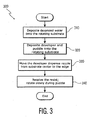
- a process 300 may be used to develop an exposed photo resist coated substrate.
- de-ionized water is deposited onto the rotating substrate 310.
- Developer is deposited and puddled onto the rotating substrate 320.
- the developer dispense nozzle is moved from substrate center to the edge 330.
- the developer is modified. Therefore, local differences of resist features may result in local differences of development rate. These differences are minimized by agitation achieved by slow rotation during puddle 340.
- DI water may be substituted by other aqueous solutions.
- aqueous solutions may include but are not limited to organic ammonium hydroxide, metal hydroxides, alcohols, amines, and surfactants.
- TMAH tetra-methyl-ammonia hydroxide
- an exposed photo resist-coated substrate may be developed.
- a process 400 is depicted in a multi-axis plot.
- Spin speed 410 in revolutions per minute (RPM) and dispense nozzle arm position 430 are plotted against time 420 in seconds (S).
- RPM revolutions per minute
- S time 420 in seconds
- a wafer having been printed with desired circuit features is placed within a develop apparatus.
- This apparatus has a vacuum platen that holds the wafer in place as it is spun.
- the wafer initially receives a DI water pre-wet dispense 440 and is spun at about 800 rpm for about 5 to 10 seconds.
- the spin speed is reduced to about 250 rpm and TMAH is dispensed 441 (at about 8 seconds) on the exposed photo resist surface on the wafer.
- the DI water puddles with the TMAH for about 2 seconds, after which TMAH is dispensed 442 for about another 10 to 12 seconds, at a speed of about 250 rpm.
- TMAH dispensed 442
- the TMAH dispense 442 the wafer is spun at about 10 rpm for about 60 seconds.
- the dynamic puddle 443 provides for even development of features, especially neighboring lines 210 as was depicted in FIGS. 2A and 2B .
- the wafer is subjected to a DI water rinse for about 20 seconds with the speed ramped up from about 10 rpm to about 1200 rpm.
- the DI water for the rinse may be supplied from the same nozzle as that used for the developer or be from a separate source.
- the wafer is goes through a spin-dry cycle at a speed of about 1200 to about 2500 rpm.
- the developed features having been rendered onto the photo resist the wafer is ready to undergo subsequent processing.
Landscapes
- Physics & Mathematics (AREA)
- General Physics & Mathematics (AREA)
- Photosensitive Polymer And Photoresist Processing (AREA)
- Exposure Of Semiconductors, Excluding Electron Or Ion Beam Exposure (AREA)
- Application Of Or Painting With Fluid Materials (AREA)
- Compounds Of Alkaline-Earth Elements, Aluminum Or Rare-Earth Metals (AREA)
- Processing Of Solid Wastes (AREA)
Claims (11)
- Verfahren (300) zum Entwickeln einer belichteten Fotoresistoberfläche auf einem Substrat, auszuführen in einer Prozessapparatur, wobei das Verfahren umfasst:- Platzieren (310) des Substrats auf einer Auflageplatte und Drehen der Auflageplatte,- Aufbringen (320) eines Netzmittels aus einer Auftragsdüse auf die belichtete Fotoresistoberfläche während des Drehens der Auftragsplatte,- Aufbringen von Entwickler aus der Auftragsdüse auf die belichtete Fotoresistoberfläche, wobei sich der Entwickler mit dem auf der Fotoresistoberfläche vorhandenen Netzmittel vermischt, der Wafer bei einer ersten niedrigen Geschwindigkeit gedreht wird, die Auftragsdüse sich wiederholt von Wafermitte zu Waferkante bewegt (330), wobei eine Lache aus Entwickler/Netzmittel gebildet wird, welche die belichtete Fotoresistoberfläche bedeckt, und- Bewegen (340) der Lache aus Entwickler/Netzmittel, welche die belichtete Fotoresistoberfläche auf dem Substrat bedeckt, durch eine zweite Drehung mit niedriger Geschwindigkeit, wobei die Mischung aus Entwickler/Netzmittel den belichteten Fotoresist entwickelt.
- Das Verfahren nach Anspruch 1, weiterhin umfassend Abspülen des die belichtete Fotoresistoberfläche bedeckenden Entwicklers/Netzmittels mit Reinwasser, während das Substrat bei einer hohen Geschwindigkeit gedreht wird, und Trockenschleudern des Wafersubstrats.
- Das Verfahren nach Anspruch 1, wobei das Netzmittel Reinwasser ist.
- Das Verfahren nach Anspruch 1, wobei das Netzmittel eine wässrige Lösung ist, die zumindest eines ausgewählt aus der Gruppe einschließend Ammoniumhydroxid, Metallhydroxide, Alkohole, Amine und grenzflächenaktive Stoffe enthält.
- Das Verfahren nach Anspruch 1, wobei der Entwickler eine wässrige Lösung ist, die zumindest eines ausgewählt aus der Gruppe einschließend Tetramethylammoniumhydroxid und Methallhydroxide enthält.
- Verfahren zum Entwickeln einer belichteten Fotoresistoberftäche auf einem Halbleiterwafer, wobei das Verfahren umfasst:- Aufbringen von entionisiertem Wasser auf die belichtete Fotoresistoberfläche, während der Halbleiterwafer gedreht wird,- Aufbringen von Entwickler auf die belichtete Fotoresistoberfläche, wobei sich der Entwickler mit dem auf der Fotoresistoberfläche vorhandenen entionisierten Wasser vermischt, der Wafer bei einer ersten niedrigen Geschwindigkeit gedreht wird, die Auftragsdüse sich wiederholt von Wafermitte zu Waferkante bewegt, wobei eine Lache aus Entwickler/entionisiertem Wasser gebildet wird, welche die belichtete Fotoresistoberfläche bedeckt,- Bewegen der Lache aus Entwickler/entionisiertem Wasser, welche die belichtete Fotoresistoberfläche auf dem Substrat bedeckt, durch eine zweite Drehung mit niedriger Geschwindigkeit, wobei die Mischung aus Entwickler/entionisiertem Wasser den belichteten Fotoresist entwickelt,- Abspülen des die belichtete Fotoresistoberfläche bedeckenden Entwicklers/entionisierten Wassers mit entionisiertem Wasser, während das der Halbleiterwafer bei einer hohen Geschwindigkeit gedreht wird, und- Trockenschleudern des Halbleiterwafers.
- Das Verfahren zum Entwickeln von belichtetem Fotoresist auf einem Halbleiterwafer nach Anspruch 6, wobei der Entwickler eine wässrige Lösung ist, die zumindest eines ausgewählt aus der Gruppe einschließend Tetramethylammoniumhydroxid und Methallhydroxide enthält.
- Verfahren zum Herstellen eines Halbleiterbauelements, umfassend: Auftragen einer Fotoresistoberfläche auf einen Halbleiterwafer,- Belichten der Fotoresistoberfläche mit Licht, um ein Schaltungsmuster zu erhalten, Platzieren des Halbleiterwafers in eine Prozessapparatur,- Drehen des Halbleiterwafers während des Aufbringens von entionisiertem Wasser auf die Fotoresistoberfläche,- Aufbringen von Entwickler aus einer Auftragsdüse in der Prozessapparatur auf die Fotoresistoberfläche, wobei sich der Entwickler mit dem auf der Fotoresistoberfläche vorhandenen entionisierten Wasser vermischt, der Halbleiterwafer bei einer ersten niedrigen Geschwindigkeit gedreht wird, die Auftragsdüse sich wiederholt von Wafermitte zu Waferkante bewegt, wobei eine Lache aus Entwickler/entionisiertem Wasser gebildet wird, welche die Fotoresistoberfläche bedeckt, und- Bewegen der Lache aus Entwickler/entionisiertem Wasser, welche die Fotoresistoberfläche auf dem Halbleiterwafer bedeckt, durch eine zweite Drehung mit niedriger Geschwindigkeit, wodurch der Fotoresist entwickelt wird.
- Das Verfahren zum Herstellen eines Halbleiterbauelements nach Anspruch 8, weiterhin umfassend Abspülen der die Fotoresistoberfläche bedeckenden Lache aus Entwickler/entionisiertem Wasser mit entionisiertem Wasser nach Entwickeln des Fotoresists, während der Halbleiterwafer bei einer hohen Geschwindigkeit gedreht wird, und Trockenschleudern des Wafersubstrats.
- Halbleiterbauteil, hergestellt nach dem Verfahren nach Anspruch 9.
- System zum Herstellen eines Halbleiterbauteils, wobei das System umfasst:- Mittel zum Auftragen einer Fotoresistoberfläche auf einen Halbleiterwafer,- Mittel zum Belichten der Fotoresistoberfläche mit Licht, um ein Schaltungsmuster zu erhalten;- Mittel zum Drehen des Halbleiterwafers während des Aufbringens von entionisiertem Wasser auf die Fotoresistoberfläche,- Mittel zum Aufbringen von Entwickler auf die Fotoresistoberfläche, wobei sich der Entwickler mit dem auf der Fotoresistoberfläche vorhandenen entionisierten Wasser vermischt, der Wafer bei einer ersten niedrigen Geschwindigkeit gedreht wird, die Auftragsdüse sich wiederholt von Wafermitte zu Waferkante bewegt, wobei eine Lache aus Entwickler/entionisiertem Wasser gebildet wird, welche die belichtete Fotoresistoberfläche bedeckt, und Mittel zum Bewegen der Lache aus Entwickler/entionisiertem Wasser, welche die belichtete Fotoresistoberfläche auf dem Halbleiterwafer bedeckt, durch eine zweite Drehung mit niedriger Geschwindigkeit, wodurch der Fotoresist entwickelt wird.
Applications Claiming Priority (2)
| Application Number | Priority Date | Filing Date | Title |
|---|---|---|---|
| US62091504P | 2004-10-20 | 2004-10-20 | |
| PCT/IB2005/053449 WO2006043253A2 (en) | 2004-10-20 | 2005-10-20 | Dynamic development process with de-ionized water puddle |
Publications (2)
| Publication Number | Publication Date |
|---|---|
| EP1812825A2 EP1812825A2 (de) | 2007-08-01 |
| EP1812825B1 true EP1812825B1 (de) | 2009-04-22 |
Family
ID=36203334
Family Applications (1)
| Application Number | Title | Priority Date | Filing Date |
|---|---|---|---|
| EP05819484A Expired - Lifetime EP1812825B1 (de) | 2004-10-20 | 2005-10-20 | Dynamischer entwicklungsprozess mit einer entionisierten wasserlache |
Country Status (6)
| Country | Link |
|---|---|
| EP (1) | EP1812825B1 (de) |
| JP (1) | JP2008517476A (de) |
| AT (1) | ATE429665T1 (de) |
| DE (1) | DE602005014132D1 (de) |
| TW (1) | TW200627549A (de) |
| WO (1) | WO2006043253A2 (de) |
Families Citing this family (2)
| Publication number | Priority date | Publication date | Assignee | Title |
|---|---|---|---|---|
| US10459340B2 (en) | 2014-12-01 | 2019-10-29 | Tokyo Electron Limited | Developing method, computer-readable storage medium and developing apparatus |
| JP6370282B2 (ja) * | 2015-09-25 | 2018-08-08 | 東京エレクトロン株式会社 | 現像処理方法及び現像処理装置 |
Family Cites Families (5)
| Publication number | Priority date | Publication date | Assignee | Title |
|---|---|---|---|---|
| JPH10303106A (ja) * | 1997-04-30 | 1998-11-13 | Toshiba Corp | 現像処理装置およびその処理方法 |
| US6265323B1 (en) * | 1998-02-23 | 2001-07-24 | Kabushiki Kaisha Toshiba | Substrate processing method and apparatus |
| US6159662A (en) * | 1999-05-17 | 2000-12-12 | Taiwan Semiconductor Manufacturing Company | Photoresist development method with reduced cycle time and improved performance |
| JP3362781B2 (ja) * | 2000-02-03 | 2003-01-07 | 日本電気株式会社 | 現像処理方法および装置、現像制御装置、情報記憶媒体 |
| US20040072450A1 (en) * | 2002-10-15 | 2004-04-15 | Collins Jimmy D. | Spin-coating methods and apparatuses for spin-coating, including pressure sensor |
-
2005
- 2005-10-17 TW TW094136203A patent/TW200627549A/zh unknown
- 2005-10-20 EP EP05819484A patent/EP1812825B1/de not_active Expired - Lifetime
- 2005-10-20 JP JP2007537465A patent/JP2008517476A/ja not_active Withdrawn
- 2005-10-20 AT AT05819484T patent/ATE429665T1/de not_active IP Right Cessation
- 2005-10-20 DE DE602005014132T patent/DE602005014132D1/de not_active Expired - Lifetime
- 2005-10-20 WO PCT/IB2005/053449 patent/WO2006043253A2/en not_active Ceased
Also Published As
| Publication number | Publication date |
|---|---|
| WO2006043253A2 (en) | 2006-04-27 |
| DE602005014132D1 (de) | 2009-06-04 |
| EP1812825A2 (de) | 2007-08-01 |
| ATE429665T1 (de) | 2009-05-15 |
| TW200627549A (en) | 2006-08-01 |
| JP2008517476A (ja) | 2008-05-22 |
| WO2006043253A3 (en) | 2007-08-30 |
Similar Documents
| Publication | Publication Date | Title |
|---|---|---|
| KR100434485B1 (ko) | 포토레지스트 스트립퍼 조성물 및 이를 이용한 포토레지스트 스트립 방법 | |
| US7846623B2 (en) | Resist pattern and reflow technology | |
| US5091290A (en) | Process for promoting adhesion of a layer of photoresist on a substrate having a previous layer of photoresist | |
| KR20020035169A (ko) | 패턴의 제조방법 | |
| JPH09326361A (ja) | レジスト現像処理方法 | |
| US6210846B1 (en) | Exposure during rework for enhanced resist removal | |
| US5780105A (en) | Method for uniformly coating a semiconductor wafer with photoresist | |
| US20020187437A1 (en) | Development method for manufacturing semiconductors | |
| US20170205712A1 (en) | Development apparatus and method for developing photoresist layer on wafer using the same | |
| US6780736B1 (en) | Method for image reversal of implant resist using a single photolithography exposure and structures formed thereby | |
| WO2007074862A1 (ja) | ホトリソグラフィ用洗浄液およびその循環使用方法 | |
| EP1812825B1 (de) | Dynamischer entwicklungsprozess mit einer entionisierten wasserlache | |
| US8518634B2 (en) | Cleaning process for semiconductor device fabrication | |
| US5296333A (en) | Photoresist adhesion promoter | |
| US20250069881A1 (en) | Method for reducing charging of semiconductor wafers | |
| JPH11288877A (ja) | レジストパターンの形成方法及び微細加工方法 | |
| JPH03215867A (ja) | ポジレジストの現像処理方法 | |
| US8338082B2 (en) | DI water rinse of photoresists with insoluble dye content | |
| KR100269318B1 (ko) | 웨이퍼상에형성된감광막의현상방법 | |
| KR100441708B1 (ko) | 포토리소그래피 공정에서의 현상방법 | |
| Mishra | Photoresist development on sic and its use as an etch mask for sic plasma etch | |
| KR100641538B1 (ko) | 반도체 제조용 현상 방법 | |
| KR20000017439A (ko) | 습식 처리에 따른 레지스트막 현상 공정을 구비하는 반도체장치의 제조방법 | |
| JPH021298B2 (de) | ||
| KR19990035265A (ko) | 반도체 감광막의 현상방법 |
Legal Events
| Date | Code | Title | Description |
|---|---|---|---|
| PUAI | Public reference made under article 153(3) epc to a published international application that has entered the european phase |
Free format text: ORIGINAL CODE: 0009012 |
|
| AK | Designated contracting states |
Kind code of ref document: A2 Designated state(s): AT BE BG CH CY CZ DE DK EE ES FI FR GB GR HU IE IS IT LI LT LU LV MC NL PL PT RO SE SI SK TR |
|
| AX | Request for extension of the european patent |
Extension state: AL BA HR MK YU |
|
| R17D | Deferred search report published (corrected) |
Effective date: 20070830 |
|
| DAX | Request for extension of the european patent (deleted) | ||
| 17P | Request for examination filed |
Effective date: 20080229 |
|
| RBV | Designated contracting states (corrected) |
Designated state(s): AT BE BG CH CY CZ DE DK EE ES FI FR GB GR HU IE IS IT LI LT LU LV MC NL PL PT RO SE SI SK TR |
|
| 17Q | First examination report despatched |
Effective date: 20080409 |
|
| RAP1 | Party data changed (applicant data changed or rights of an application transferred) |
Owner name: NXP B.V. |
|
| GRAP | Despatch of communication of intention to grant a patent |
Free format text: ORIGINAL CODE: EPIDOSNIGR1 |
|
| RAP1 | Party data changed (applicant data changed or rights of an application transferred) |
Owner name: NXP B.V. |
|
| GRAP | Despatch of communication of intention to grant a patent |
Free format text: ORIGINAL CODE: EPIDOSNIGR1 |
|
| GRAS | Grant fee paid |
Free format text: ORIGINAL CODE: EPIDOSNIGR3 |
|
| GRAA | (expected) grant |
Free format text: ORIGINAL CODE: 0009210 |
|
| AK | Designated contracting states |
Kind code of ref document: B1 Designated state(s): AT BE BG CH CY CZ DE DK EE ES FI FR GB GR HU IE IS IT LI LT LU LV MC NL PL PT RO SE SI SK TR |
|
| REG | Reference to a national code |
Ref country code: GB Ref legal event code: FG4D |
|
| REG | Reference to a national code |
Ref country code: CH Ref legal event code: EP |
|
| REG | Reference to a national code |
Ref country code: IE Ref legal event code: FG4D |
|
| REF | Corresponds to: |
Ref document number: 602005014132 Country of ref document: DE Date of ref document: 20090604 Kind code of ref document: P |
|
| NLV1 | Nl: lapsed or annulled due to failure to fulfill the requirements of art. 29p and 29m of the patents act | ||
| PG25 | Lapsed in a contracting state [announced via postgrant information from national office to epo] |
Ref country code: PT Free format text: LAPSE BECAUSE OF FAILURE TO SUBMIT A TRANSLATION OF THE DESCRIPTION OR TO PAY THE FEE WITHIN THE PRESCRIBED TIME-LIMIT Effective date: 20090822 Ref country code: FI Free format text: LAPSE BECAUSE OF FAILURE TO SUBMIT A TRANSLATION OF THE DESCRIPTION OR TO PAY THE FEE WITHIN THE PRESCRIBED TIME-LIMIT Effective date: 20090422 Ref country code: ES Free format text: LAPSE BECAUSE OF FAILURE TO SUBMIT A TRANSLATION OF THE DESCRIPTION OR TO PAY THE FEE WITHIN THE PRESCRIBED TIME-LIMIT Effective date: 20090802 Ref country code: AT Free format text: LAPSE BECAUSE OF FAILURE TO SUBMIT A TRANSLATION OF THE DESCRIPTION OR TO PAY THE FEE WITHIN THE PRESCRIBED TIME-LIMIT Effective date: 20090422 Ref country code: LT Free format text: LAPSE BECAUSE OF FAILURE TO SUBMIT A TRANSLATION OF THE DESCRIPTION OR TO PAY THE FEE WITHIN THE PRESCRIBED TIME-LIMIT Effective date: 20090422 |
|
| PG25 | Lapsed in a contracting state [announced via postgrant information from national office to epo] |
Ref country code: NL Free format text: LAPSE BECAUSE OF FAILURE TO SUBMIT A TRANSLATION OF THE DESCRIPTION OR TO PAY THE FEE WITHIN THE PRESCRIBED TIME-LIMIT Effective date: 20090422 Ref country code: PL Free format text: LAPSE BECAUSE OF FAILURE TO SUBMIT A TRANSLATION OF THE DESCRIPTION OR TO PAY THE FEE WITHIN THE PRESCRIBED TIME-LIMIT Effective date: 20090422 Ref country code: SE Free format text: LAPSE BECAUSE OF FAILURE TO SUBMIT A TRANSLATION OF THE DESCRIPTION OR TO PAY THE FEE WITHIN THE PRESCRIBED TIME-LIMIT Effective date: 20090722 Ref country code: SI Free format text: LAPSE BECAUSE OF FAILURE TO SUBMIT A TRANSLATION OF THE DESCRIPTION OR TO PAY THE FEE WITHIN THE PRESCRIBED TIME-LIMIT Effective date: 20090422 Ref country code: LV Free format text: LAPSE BECAUSE OF FAILURE TO SUBMIT A TRANSLATION OF THE DESCRIPTION OR TO PAY THE FEE WITHIN THE PRESCRIBED TIME-LIMIT Effective date: 20090422 Ref country code: IS Free format text: LAPSE BECAUSE OF FAILURE TO SUBMIT A TRANSLATION OF THE DESCRIPTION OR TO PAY THE FEE WITHIN THE PRESCRIBED TIME-LIMIT Effective date: 20090822 |
|
| PG25 | Lapsed in a contracting state [announced via postgrant information from national office to epo] |
Ref country code: RO Free format text: LAPSE BECAUSE OF FAILURE TO SUBMIT A TRANSLATION OF THE DESCRIPTION OR TO PAY THE FEE WITHIN THE PRESCRIBED TIME-LIMIT Effective date: 20090422 Ref country code: DK Free format text: LAPSE BECAUSE OF FAILURE TO SUBMIT A TRANSLATION OF THE DESCRIPTION OR TO PAY THE FEE WITHIN THE PRESCRIBED TIME-LIMIT Effective date: 20090422 Ref country code: EE Free format text: LAPSE BECAUSE OF FAILURE TO SUBMIT A TRANSLATION OF THE DESCRIPTION OR TO PAY THE FEE WITHIN THE PRESCRIBED TIME-LIMIT Effective date: 20090422 Ref country code: CZ Free format text: LAPSE BECAUSE OF FAILURE TO SUBMIT A TRANSLATION OF THE DESCRIPTION OR TO PAY THE FEE WITHIN THE PRESCRIBED TIME-LIMIT Effective date: 20090422 |
|
| PG25 | Lapsed in a contracting state [announced via postgrant information from national office to epo] |
Ref country code: SK Free format text: LAPSE BECAUSE OF FAILURE TO SUBMIT A TRANSLATION OF THE DESCRIPTION OR TO PAY THE FEE WITHIN THE PRESCRIBED TIME-LIMIT Effective date: 20090422 Ref country code: BE Free format text: LAPSE BECAUSE OF FAILURE TO SUBMIT A TRANSLATION OF THE DESCRIPTION OR TO PAY THE FEE WITHIN THE PRESCRIBED TIME-LIMIT Effective date: 20090422 |
|
| PLBE | No opposition filed within time limit |
Free format text: ORIGINAL CODE: 0009261 |
|
| STAA | Information on the status of an ep patent application or granted ep patent |
Free format text: STATUS: NO OPPOSITION FILED WITHIN TIME LIMIT |
|
| 26N | No opposition filed |
Effective date: 20100125 |
|
| PG25 | Lapsed in a contracting state [announced via postgrant information from national office to epo] |
Ref country code: BG Free format text: LAPSE BECAUSE OF FAILURE TO SUBMIT A TRANSLATION OF THE DESCRIPTION OR TO PAY THE FEE WITHIN THE PRESCRIBED TIME-LIMIT Effective date: 20090722 |
|
| PG25 | Lapsed in a contracting state [announced via postgrant information from national office to epo] |
Ref country code: MC Free format text: LAPSE BECAUSE OF NON-PAYMENT OF DUE FEES Effective date: 20091031 |
|
| REG | Reference to a national code |
Ref country code: CH Ref legal event code: PL |
|
| PG25 | Lapsed in a contracting state [announced via postgrant information from national office to epo] |
Ref country code: CH Free format text: LAPSE BECAUSE OF NON-PAYMENT OF DUE FEES Effective date: 20091031 Ref country code: GR Free format text: LAPSE BECAUSE OF FAILURE TO SUBMIT A TRANSLATION OF THE DESCRIPTION OR TO PAY THE FEE WITHIN THE PRESCRIBED TIME-LIMIT Effective date: 20090723 Ref country code: IE Free format text: LAPSE BECAUSE OF NON-PAYMENT OF DUE FEES Effective date: 20091020 Ref country code: LI Free format text: LAPSE BECAUSE OF NON-PAYMENT OF DUE FEES Effective date: 20091031 |
|
| PG25 | Lapsed in a contracting state [announced via postgrant information from national office to epo] |
Ref country code: IT Free format text: LAPSE BECAUSE OF FAILURE TO SUBMIT A TRANSLATION OF THE DESCRIPTION OR TO PAY THE FEE WITHIN THE PRESCRIBED TIME-LIMIT Effective date: 20090422 |
|
| PG25 | Lapsed in a contracting state [announced via postgrant information from national office to epo] |
Ref country code: LU Free format text: LAPSE BECAUSE OF NON-PAYMENT OF DUE FEES Effective date: 20091020 |
|
| PG25 | Lapsed in a contracting state [announced via postgrant information from national office to epo] |
Ref country code: HU Free format text: LAPSE BECAUSE OF FAILURE TO SUBMIT A TRANSLATION OF THE DESCRIPTION OR TO PAY THE FEE WITHIN THE PRESCRIBED TIME-LIMIT Effective date: 20091023 |
|
| PG25 | Lapsed in a contracting state [announced via postgrant information from national office to epo] |
Ref country code: TR Free format text: LAPSE BECAUSE OF FAILURE TO SUBMIT A TRANSLATION OF THE DESCRIPTION OR TO PAY THE FEE WITHIN THE PRESCRIBED TIME-LIMIT Effective date: 20090422 |
|
| PG25 | Lapsed in a contracting state [announced via postgrant information from national office to epo] |
Ref country code: CY Free format text: LAPSE BECAUSE OF FAILURE TO SUBMIT A TRANSLATION OF THE DESCRIPTION OR TO PAY THE FEE WITHIN THE PRESCRIBED TIME-LIMIT Effective date: 20090422 |
|
| PGFP | Annual fee paid to national office [announced via postgrant information from national office to epo] |
Ref country code: GB Payment date: 20120924 Year of fee payment: 8 |
|
| PGFP | Annual fee paid to national office [announced via postgrant information from national office to epo] |
Ref country code: FR Payment date: 20121115 Year of fee payment: 8 |
|
| GBPC | Gb: european patent ceased through non-payment of renewal fee |
Effective date: 20131020 |
|
| PG25 | Lapsed in a contracting state [announced via postgrant information from national office to epo] |
Ref country code: GB Free format text: LAPSE BECAUSE OF NON-PAYMENT OF DUE FEES Effective date: 20131020 |
|
| REG | Reference to a national code |
Ref country code: FR Ref legal event code: ST Effective date: 20140630 |
|
| PG25 | Lapsed in a contracting state [announced via postgrant information from national office to epo] |
Ref country code: FR Free format text: LAPSE BECAUSE OF NON-PAYMENT OF DUE FEES Effective date: 20131031 |
|
| PGFP | Annual fee paid to national office [announced via postgrant information from national office to epo] |
Ref country code: DE Payment date: 20170920 Year of fee payment: 13 |
|
| REG | Reference to a national code |
Ref country code: DE Ref legal event code: R119 Ref document number: 602005014132 Country of ref document: DE |
|
| PG25 | Lapsed in a contracting state [announced via postgrant information from national office to epo] |
Ref country code: DE Free format text: LAPSE BECAUSE OF NON-PAYMENT OF DUE FEES Effective date: 20190501 |