EP1816736A2 - Elektrische Stromwandlervorrichtung - Google Patents
Elektrische Stromwandlervorrichtung Download PDFInfo
- Publication number
- EP1816736A2 EP1816736A2 EP06026365A EP06026365A EP1816736A2 EP 1816736 A2 EP1816736 A2 EP 1816736A2 EP 06026365 A EP06026365 A EP 06026365A EP 06026365 A EP06026365 A EP 06026365A EP 1816736 A2 EP1816736 A2 EP 1816736A2
- Authority
- EP
- European Patent Office
- Prior art keywords
- voltage
- pwm
- pulse
- output voltage
- value
- Prior art date
- Legal status (The legal status is an assumption and is not a legal conclusion. Google has not performed a legal analysis and makes no representation as to the accuracy of the status listed.)
- Granted
Links
Images











Classifications
-
- H—ELECTRICITY
- H02—GENERATION; CONVERSION OR DISTRIBUTION OF ELECTRIC POWER
- H02M—APPARATUS FOR CONVERSION BETWEEN AC AND AC, BETWEEN AC AND DC, OR BETWEEN DC AND DC, AND FOR USE WITH MAINS OR SIMILAR POWER SUPPLY SYSTEMS; CONVERSION OF DC OR AC INPUT POWER INTO SURGE OUTPUT POWER; CONTROL OR REGULATION THEREOF
- H02M7/00—Conversion of AC power input into DC power output; Conversion of DC power input into AC power output
- H02M7/42—Conversion of DC power input into AC power output without possibility of reversal
- H02M7/44—Conversion of DC power input into AC power output without possibility of reversal by static converters
- H02M7/48—Conversion of DC power input into AC power output without possibility of reversal by static converters using discharge tubes with control electrode or semiconductor devices with control electrode
- H02M7/53—Conversion of DC power input into AC power output without possibility of reversal by static converters using discharge tubes with control electrode or semiconductor devices with control electrode using devices of a triode or transistor type requiring continuous application of a control signal
- H02M7/537—Conversion of DC power input into AC power output without possibility of reversal by static converters using discharge tubes with control electrode or semiconductor devices with control electrode using devices of a triode or transistor type requiring continuous application of a control signal using semiconductor devices only, e.g. single switched pulse inverters
- H02M7/5387—Conversion of DC power input into AC power output without possibility of reversal by static converters using discharge tubes with control electrode or semiconductor devices with control electrode using devices of a triode or transistor type requiring continuous application of a control signal using semiconductor devices only, e.g. single switched pulse inverters in a bridge configuration
- H02M7/53871—Conversion of DC power input into AC power output without possibility of reversal by static converters using discharge tubes with control electrode or semiconductor devices with control electrode using devices of a triode or transistor type requiring continuous application of a control signal using semiconductor devices only, e.g. single switched pulse inverters in a bridge configuration with automatic control of output voltage or current
- H02M7/53875—Conversion of DC power input into AC power output without possibility of reversal by static converters using discharge tubes with control electrode or semiconductor devices with control electrode using devices of a triode or transistor type requiring continuous application of a control signal using semiconductor devices only, e.g. single switched pulse inverters in a bridge configuration with automatic control of output voltage or current with analogue control of three-phase output
-
- B—PERFORMING OPERATIONS; TRANSPORTING
- B60—VEHICLES IN GENERAL
- B60L—PROPULSION OF ELECTRICALLY-PROPELLED VEHICLES; SUPPLYING ELECTRIC POWER FOR AUXILIARY EQUIPMENT OF ELECTRICALLY-PROPELLED VEHICLES; ELECTRODYNAMIC BRAKE SYSTEMS FOR VEHICLES IN GENERAL; MAGNETIC SUSPENSION OR LEVITATION FOR VEHICLES; MONITORING OPERATING VARIABLES OF ELECTRICALLY-PROPELLED VEHICLES; ELECTRIC SAFETY DEVICES FOR ELECTRICALLY-PROPELLED VEHICLES
- B60L58/00—Methods or circuit arrangements for monitoring or controlling batteries or fuel cells, specially adapted for electric vehicles
- B60L58/30—Methods or circuit arrangements for monitoring or controlling batteries or fuel cells, specially adapted for electric vehicles for monitoring or controlling fuel cells
-
- H—ELECTRICITY
- H02—GENERATION; CONVERSION OR DISTRIBUTION OF ELECTRIC POWER
- H02M—APPARATUS FOR CONVERSION BETWEEN AC AND AC, BETWEEN AC AND DC, OR BETWEEN DC AND DC, AND FOR USE WITH MAINS OR SIMILAR POWER SUPPLY SYSTEMS; CONVERSION OF DC OR AC INPUT POWER INTO SURGE OUTPUT POWER; CONTROL OR REGULATION THEREOF
- H02M7/00—Conversion of AC power input into DC power output; Conversion of DC power input into AC power output
- H02M7/42—Conversion of DC power input into AC power output without possibility of reversal
- H02M7/44—Conversion of DC power input into AC power output without possibility of reversal by static converters
- H02M7/48—Conversion of DC power input into AC power output without possibility of reversal by static converters using discharge tubes with control electrode or semiconductor devices with control electrode
- H02M7/483—Converters with outputs that each can have more than two voltages levels
-
- Y—GENERAL TAGGING OF NEW TECHNOLOGICAL DEVELOPMENTS; GENERAL TAGGING OF CROSS-SECTIONAL TECHNOLOGIES SPANNING OVER SEVERAL SECTIONS OF THE IPC; TECHNICAL SUBJECTS COVERED BY FORMER USPC CROSS-REFERENCE ART COLLECTIONS [XRACs] AND DIGESTS
- Y02—TECHNOLOGIES OR APPLICATIONS FOR MITIGATION OR ADAPTATION AGAINST CLIMATE CHANGE
- Y02T—CLIMATE CHANGE MITIGATION TECHNOLOGIES RELATED TO TRANSPORTATION
- Y02T90/00—Enabling technologies or technologies with a potential or indirect contribution to GHG emissions mitigation
- Y02T90/40—Application of hydrogen technology to transportation, e.g. using fuel cells
Definitions
- the present invention relates generally to electric power conversion apparatuses and methods, and more particularly to electric power conversion apparatuses and methods adapted to be electrically connected to a plurality of power supplies.
- JP2002-118981 shows an electric power conversion system which employs a fuel cell as a main power supply and a battery as a sub power supply to drive an electric motor. While the fuel cell is connected electrically and directly to the motor, the battery is electrically connected to the motor via a DCDC (Direct Current to Direct Current) converter. The output voltage of the DCDC converter is controlled in order to improve the output efficiency of the power supplies.
- DCDC Direct Current to Direct Current
- the provision of the DCDC converter causes an increase in the size of the whole system including the power supplies, the electric power conversion system and the motor, and causes a power loss due to the DCDC converter in charging and discharging the battery.
- an object of the present invention to provide an electric power conversion apparatus and method which employs a plurality of power supplies (not limited to the combination of fuel cell and battery) in no need of a separate DCDC converter, and accordingly which is constructed compact and operates with a minimum power loss.
- an electric power conversion apparatus comprises: a power converter adapted to be electrically connected to at least a first DC voltage source, a second DC voltage source and a load including an AC electric motor, and configured to generate an individual output voltage pulse train from an output voltage of each of the DC voltage sources in accordance with a switch drive signal set, to synthesize a final output voltage from the individual output voltage pulse trains, and to drive the AC electric motor with the final output voltage; and a power-converter control unit configured to control the switch drive signal set, the power-converter control unit including a PWM pulse generation section configured to perform the following: comparing a voltage command value with a PWM carrier for each of the DC voltage sources; and generating based on the comparison a first PWM pulse train for supplying a first output voltage pulse train from the first DC voltage source to the load and a second PWM pulse train for supplying a second output voltage pulse train from the second DC voltage source to the load in such a manner to form a pulse continuous in time in the final output
- an electric power conversion apparatus comprises: power conversion means for generating an individual output voltage pulse train from an output voltage of each of first and second DC voltage sources in accordance with a switch drive signal set, to synthesize a final output voltage from the individual output voltage pulse trains, and to drive an AC electric motor included in a load with the final output voltage; and control means for controlling the switch drive signal set, the control means including PWM pulse generation means for performing the following: comparing a voltage command value with a PWM carrier for each of the DC voltage sources; and generating based on the comparison a first PWM pulse train for supplying a first output voltage pulse train from the first DC voltage source to the load and a second PWM pulse train for supplying a second output voltage pulse train from the second DC voltage source to the load in such a manner to form a pulse continuous in time in the final output voltage at least from each pulse of the first output voltage pulse train and a subsequent pulse of the second output voltage pulse train.
- a method for controlling an electric power conversion apparatus comprising a power converter adapted to be electrically connected to at least a first DC voltage source, a second DC voltage source and a load including an AC electric motor, and configured to generate an individual output voltage pulse train from an output voltage of each of the DC voltage sources in accordance with a switch drive signal set, to synthesize a final output voltage from the individual output voltage pulse trains, and to drive the AC electric motor with the final output voltage, and a power-converter control unit configured to control the switch drive signal set, comprises: comparing a voltage command value with a PWM carrier for each of the DC voltage sources; and generating based on the comparison a first PWM pulse train for supplying a first output voltage pulse train from the first DC voltage source to the load and a second PWM pulse train for supplying a second output voltage pulse train from the second DC voltage source to the load in such a manner to form a pulse continuous in time in the final output voltage at least from each pulse of the first output voltage pulse train and
- FIG. 1 is a schematic circuit diagram showing a power converter of an electric power conversion apparatus in accordance with a first embodiment of the present invention.
- FIG. 2 is a schematic block diagram showing the electric power conversion apparatus of the first embodiment.
- FIG. 3 is a schematic block diagram showing a motor-current control section of the electric power conversion apparatus of FIG. 2.
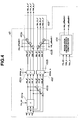
- FIG. 4 is a schematic block diagram showing a power-control/modulation-factor-computation section of the electric power conversion apparatus of FIG. 2.
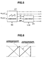
- FIG. 5 is a schematic block diagram showing a PWM (Pulse Width Modulation) pulse generation section of the electric power conversion apparatus of FIG. 2.
- PWM Pulse Width Modulation
- FIG. 6 is a diagram showing the waveform of PWM carriers employed in the PWM pulse generation section of FIG. 5, where the PWM carriers each have a sawtooth waveform.
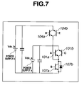
- FIG. 7 is a schematic circuit diagram showing a U-phase section of the power converter of FIG. 1.
- FIGS. 8A to 8F are diagrams showing an example of switch drive signals generated based on comparison between a U-phase instantaneous modulation factor command value and the sawtooth PWM carriers of FIG. 6.
- FIG. 9 is a logic circuit diagram showing a process for the switch drive signals of FIGS. 8A to 8F.
- FIGS. 10A to 10G are diagrams showing an example of a process of generating a signal OVR with respect to the other switch drive signals in the first embodiment.
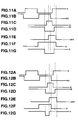
- FIGS. 11A to 11G are diagrams showing an example of a process of generating switch drive signals E and C based on comparison in magnitude between the output voltages of DC voltage sources.
- FIGS. 12A to 12G are diagrams showing another example of the process of generating switch drive signals E and C based on comparison in magnitude between the output voltages of the DC voltage sources.
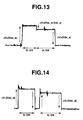
- FIG. 13 is a diagram showing an experimental example in which the electric power conversion apparatus outputs an output voltage containing a continuous pulse based on the two DC voltage sources in the first embodiment.
- FIG. 14 is a diagram showing an experimental example in which separated pulses are outputted based on the two DC voltage sources in a comparative example.
- FIG. 15 is a diagram showing the waveform of PWM carriers employed in the PWM pulse generation section of an electric power conversion apparatus in accordance with a second embodiment of the present invention, where the PWM carriers have sawtooth waveforms with a phase shift.
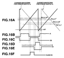
- FIGS. 16A to 16F are diagrams showing an example of switch drive signals generated based on comparison between the U-phase instantaneous modulation factor command value and the sawtooth PWM carriers of FIG. 15.
- FIGS. 17A to 17F are diagrams showing an example of signal OVR with respect to the other switch drive signals in the second embodiment.
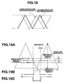
- FIG. 18 is a diagram showing the waveform of PWM carriers employed in the PWM pulse generation section of an electric power conversion apparatus in accordance with a third embodiment of the present invention, where the PWM carriers have triangular waveforms with a phase shift.
- FIGS. 19A to 19C are diagrams showing an example of a process of generating switch drive signals A and E0 based on comparison between a U-phase instantaneous modulation factor command value and the triangular PWM carriers of FIG. 18.
- FIGS. 20A to 20C are diagrams showing an example of a process of generating switch drive signals D and C0 based on comparison between the U-phase instantaneous modulation factor command value and the triangular PWM carriers of FIG. 18.
- FIG. 21 is a diagram showing how to set the phase shift between the triangular PWM carriers of FIG. 18.
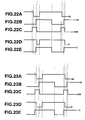
- FIGS. 22A to 22E are diagrams showing an example of a process of generating switch drive signals E and C based on comparison in magnitude between the output voltages of the DC voltage sources.
- FIGS. 23A to 23E are diagrams showing another example of the process of generating switch drive signals E and C based on comparison in magnitude between the output voltages of the DC voltage sources.
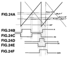
- FIGS. 24A to 24F are diagrams showing an example of switch drive signals generated based on comparison between the U-phase instantaneous modulation factor command value and the sawtooth PWM carriers.
- FIG. 25 is a schematic block diagram showing a power-control/modulation-factor-computation section of an electric power conversion apparatus in accordance with a fifth embodiment of the present invention.
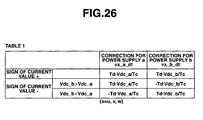
- FIG. 26 is a diagram showing a table employed by a voltage correction computation section of the power-control/modulation-factor-computation section of FIG. 25.
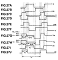
- FIGS. 27A to 27J are diagrams showing an example of a U-phase output voltage pulse train with respect to the switch drive signals in the fifth embodiment.
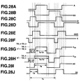
- FIGS. 28A to 28J are diagrams showing another example of the U-phase output voltage pulse train in the fifth embodiment.
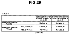
- FIG. 29 is a diagram showing a table employed by a voltage correction computation section of a power-control/modulation-factor-computation section of an electric power conversion apparatus in accordance with a fifth embodiment of the present invention.
- FIG. 30 is a schematic block diagram showing a power-control/modulation-factor-computation section of an electric power conversion apparatus in accordance with a seventh embodiment of the present invention.
- FIG. 31 is a diagram showing a table employed by a voltage correction computation section of the power-control/modulation-factor-computation section of FIG. 30.
- FIG. 32 is a diagram showing a table employed by a voltage correction computation section of a power-control/modulation-factor-computation section of an electric power conversion apparatus in accordance with an eighth embodiment of the present invention.
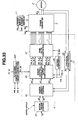
- FIG. 33 is a schematic circuit diagram showing a power converter of an electric power conversion apparatus in accordance with a ninth embodiment of the present invention.
- FIG. 34 is a graph showing a process of correction performed by an allocated power proportion target correction section of the electric power conversion apparatus of FIG. 33.
- FIG. 1 shows a schematic circuit diagram of a power converter of an electric power conversion apparatus in accordance with a first embodiment of the present invention.
- the power converter is adapted to be electrically connected to a plurality of voltage sources and to a three-phase synchronous electric motor.
- the negative pole of a DC voltage source a 11 and the negative pole of a DC voltage source b 12 are both electrically connected to a common negative bus 16.
- a power converter 3 includes a U-phase section 33, a V-phase section 34 and a W-phase section 35, each of which includes a contact adapted to be electrically connected to a respective one of the contacts of a three-phase synchronous electric motor 2.
- V-phase section 34 and W-phase section 35 are disposed a combination of a semiconductor switch 107a and a diode 107b, a combination of a semiconductor switch 108a and a diode 108b, and a combination of a semiconductor switch 109a and a diode 109b, respectively, as in the lower arm of a conventional inverter.
- the positive pole of DC voltage source a 11 is electrically connected to a positive bus 15.
- V-phase section 34 and W-phase section 35 are disposed a combination of semiconductor switches 101a and 101b, a combination of semiconductor switches 102a and 102b, and a combination of semiconductor switches 103a and 103b, respectively, each of which is adapted to be controlled to regulate a state of conductivity in each direction.
- the positive pole of DC voltage source b 12 is electrically connected to a positive bus 17.
- V-phase section 34 and W-phase section 35 are disposed a combination of semiconductor switches 104a and 104b, a combination of semiconductor switches 105a and 105b, and a combination of semiconductor switches 106a and 106b, respectively, each of which is adapted to be controlled to regulate a state of conductivity in each direction.
- a smoothing capacitor 13 is electrically connected between positive bus 15 and common negative bus 16, whereas a smoothing capacitor 14 is electrically connected between positive bus 17 and common negative bus 16.
- power converter 3 operates as a DCAC (Direct Current to Alternating Current) power converter, generating three-phase voltages applied to motor 2 based on the three electric potentials, i.e.
- DCAC Direct Current to Alternating Current
- the semiconductor switches are controlled to generate a voltage outputted to each phase of motor 2. Specifically, the semiconductor switches are controlled connect one of the plurality of electric potentials to each contact of motor 2. The proportion of the period of connection of each semiconductor switch is controlled to supply a necessary set of voltages to motor 2.
- FIG. 2 shows the system configuration of a power-converter control unit 4 of the electric power conversion apparatus.
- a motor-torque control section 41 is configured to compute a command value id* of the d-axis current of motor 2 and a command value iq* of the q-axis of motor 2 based on a motor-torque command value Te* and a motor speed value ⁇ which are given from outside.
- motor-torque control section 41 refers to stored information concerning a prepared map having an axis of Te* and an axis of ⁇ and outputs id* and iq* in accordance with given Te* and ⁇ .
- a motor-current control section 42 is configured to control the motor current based on d-axis current command value id* and q-axis current command value iq*, and based on a d-axis current measured value id and a q-axis current measured value iq outputted from a three-phase/dq transformation section 48, in order that id and iq follow id* and iq*, respectively.
- Motor-torque control section 41 finally outputs a U-phase voltage command value vu*, a V-phase voltage command value vv*, and a W-phase voltage command value vw*.
- FIG. 3 shows the detailed system configuration of motor-current control section 42.
- a motor-current controller 421 is configured to receive id* and iq* from motor-torque control section 41 and id and iq from three-phase/dq transformation section 48, and to output a d-axis voltage command value vd* and a q-axis voltage command value vq* by a feedback control process based on the PI control method, in order that id and iq follow id* and iq*, respectively.
- Three-phase/dq transformation section 48 computes a W-phase current measured value iw based on a U-phase current measured value iu and V-phase current measured value iv which are measured by current sensors, and converts iu, iv and iw into id and iq.
- a dq/three-phase transformation section 422 is configured to receive the d-axis voltage command value vd* and q-axis voltage command value vq*, and to transform them into U-phase voltage command value vu*, V-phase voltage command value vv*, and W-phase voltage command value vw*.
- a power-control/modulation-factor-computation section 45 is configured to receive an allocated power proportion target value rto_pa and an allocated power proportion target value rto_pb which are each a target value of an allocated power proportion of an associated one of DC voltage source a 11 and DC voltage source b 12, and to perform a power control process.
- the allocated power proportion target values are determined and given by an outside controller in such a manner to optimize the power proportions and to improve the total output efficiency of the DC voltage sources.
- Allocated power proportion target value rto_pa and allocated power proportion target value rto_pb are defined to have the following relationship.
- power-control/modulation-factor-computation section 45 receives only the allocated power proportion target value rto_pa and computes the allocated power proportion target value rto_pb.
- FIG. 4 shows the detailed system configuration of power-control/modulation-factor-computation section 45.
- a multiplier 451a is configured to multiply vu*, vv* and vw* with rto_pa to produce a U-phase voltage command value vu_a*, a V-phase voltage command value vv_a*, and a W-phase voltage command value vw_a* for DC voltage source a 11 as follows.
- a subtracter 451b is configured to subtract vu_a*, vv_a* or vw_a* from vu*, vv* and vw*, respectively, to produce a U-phase voltage command value vu_b*, a V-phase voltage command value vv_b*, and a W-phase voltage command value vw_b* for DC voltage source b 12 as follows.
- a modulation factor computation section 452 is configured to receive a DC voltage source voltage value Vdc_a which is a value of a voltage supplied by DC voltage source a 11 and a DC voltage source voltage value Vdc_b which is a value of a voltage supplied by DC voltage source b 12, and to generate and output instantaneous modulation factor command values mu_a*, mu_b*, mv_a*, mv_b*, mw_a* and mw_b* which are normalized voltage command values.
- modulation factor computation section 452 comprises a multiplier 452a and a multiplier 452b.
- U-phase voltage command value vu_a* for DC voltage source a 11 and U-phase voltage command value vu_b* for DC voltage source b 12 are normalized by the half value of each DC voltage value to produce a U-phase instantaneous modulation factor command value mu_a* for DC voltage source a 11 and a U-phase instantaneous modulation factor command value mu_b* for DC voltage source b 12 as follows.
- mu - ⁇ a * vu - ⁇ a * / Vdc - ⁇ a / 2
- mu - ⁇ b * vu - ⁇ b * / Vdc - ⁇ b / 2
- a modulation factor command correction section 453 is configured to correct the modulation factor command values based on allocation of the PWM period to obtain final modulation factor command values, in order to achieve actually desired voltage values.
- a modulation factor offset computation section 454 is configured to compute modulation factor offset values ma_offset0 and mb_offset0 based on Vdc_a, Vdc_b and rto_pa.
- rto_pb is calculated by the following equation which is equivalent to the previous equation.
- Modulation factor offset values ma_offset0 and mb_offset0 as thus computed are added to U-phase instantaneous modulation factor command value mu_a* for DC voltage source a 11 and U-phase instantaneous modulation factor command value mu_b* for DC voltage source b 12 in adders 453a and 453b, respectively.
- U-phase instantaneous modulation factor final command values mu_a_c* and mu_b_c* are calculated by the following equations.
- mu - ⁇ a - ⁇ c * mu - ⁇ a * + ma - ⁇ offset ⁇ 0 - 1
- mu - ⁇ b - ⁇ c * mu - ⁇ b * + mb - ⁇ offset ⁇ 0 - 1
- a PWM pulse generation section 47 is configured to compare the instantaneous modulation factor final command values with PWM carriers, and to control the state of each semiconductor switch based on the comparison by outputting a switch drive signal to each semiconductor switch.
- FIG. 5 shows the detailed configuration of PWM pulse generation section 47.
- FIG. 6 shows a PWM carrier waveform for DC voltage source a 11 and a PWM carrier waveform for DC voltage source b 12.
- the PWM carrier for DC voltage source a 11 has a sawtooth waveform used to generate a PWM pulse train to drive each switch.
- the PWM carrier for DC voltage source b 12 is similar as for DC voltage source a 11.
- a comparator 471 is configured to receive U-phase instantaneous modulation factor final command values mu_a_c* and mu_b_c* from power-control/modulation-factor-computation section 45, to compare them with the PWM carrier waveforms, to provide a dead time Hds to them, and finally to create the switch drive signals to drive the switches for the U phase.
- FIG. 7 shows the U-phase section, in which the switch drive signals for driving the switches for the U phase are identified as follows.
- FIGS. 8A to 8F show a pulse generation method to define how DC voltage source a 11 outputs a voltage pulse train. It is necessary to hold the switch drive signal A ON in order to output a PWM pulse train from DC voltage source a 11.
- switch drive signal E is conventionally held ON in order to serve as a diode, and to ensure a current path from a load including the motor 2 to the DC voltage sources.
- Vdc_a is greater than Vdc_b
- a state in which switch drive signals A and E are both ON causes a short-circuit current between the positive poles. Therefore, it is necessary to keep the switch drive signal E OFF while switch drive signal A is ON.
- switch drive signal A is turned from ON to OFF at the same instant when switch drive signal E is turned from OFF to ON, it actually causes a period in which switch drive signals A and E are both ON, because of a period in which the switch drive signal A is completely turned OFF.
- the short-circuit current flows to raise the quantity of heat released from the semiconductor switches disposed in the associated current path.
- switch drive signal E is turned from OFF to ON after a period in which the switch drive signals A and E are both OFF.
- Such a short-circuit prevention period (dead time) is provided in the voltage pulse train in such a manner to prevent the short circuit.
- a dead time is provided to the combination of switch drive signals A and E.
- a dead time is provided to the combination of switch drive signals D and C.
- a dead time is provided to the combination of switch drive signals A and B and to the combination of switch drive signals D and B, in order to prevent a short-circuit current between positive and negative poles.
- a short-circuit prevention period is provided for rise or fall of output voltage pulses generated by the switches in such a manner to prevent a short circuit between electric poles having different electric potentials.
- an intermediate switch drive signal E0 is generated based on comparison with the sawtooth PWM carrier.
- a value mu_a_c_down* is determined by adding a downward offset to mu_a_c* corresponding to the dead time as follows.
- mu - ⁇ a - ⁇ c - ⁇ down * mu - ⁇ a - ⁇ c * - Hds
- m0* is determined as follows.
- m ⁇ 0 * 1 - Hds
- Switch drive signals A and E0 are determined by comparing mu_a_c*, mu_a_c_down* and m0* with the PWM carrier as follows.
- a value mu_b_c_down* is determined by adding a downward offset to mu_b_c* corresponding to the dead time as follows.
- mu - ⁇ b - ⁇ c - ⁇ down * mu - ⁇ b - ⁇ c * - Hds
- Switch drive signals D and C0 are determined by comparing mu_b_c*, mu_b_c_down* and m0* with the PWM carrier as follows.
- Switch drive signal B as shown in FIG. 8F is generated by receiving the switch drive signals E0 and C0 from comparator 471 and performing a logical AND of switch drive signals E0 and C0 in logic circuit section 472 shown in FIGS. 5 and 9.
- B E ⁇ 0 ⁇ C ⁇ 0
- each pulse of switch drive signal A and an associated pulse of switch drive signal D are continuous in time.
- the associated switches are controlled in such a manner that at least one of the switches is in the ON state during switching operation between the DC voltage sources. Accordingly, the voltage pulse outputted from DC voltage source a 11 and the voltage pulse outputted from DC voltage source b 12 form a continuous voltage pulse.
- switch drive signals E0 and C0 are both OFF. If switch drive signals E0 and C0 are used as switch drive signals E and C, and if the both switch drive signals are turned OFF when the current is flowing from motor 2 to the DC voltage sources, a voltage is generated at the contact by the inductance of motor 2 and the time differential of the current value. Accordingly, in such a case, it is necessary to set the withstand voltage of each semiconductor switch in consideration of this generated voltage.
- the current path from motor 2 to at least one of the DC voltage sources is constantly provided by controlling the ON/OFF state of each semiconductor switch, in order to minimize the voltage generated at the contact and thereby to reduce the manufacturing cost of the semiconductor switches.
- switch drive signals E0 and C0 are corrected in such a manner to prevent the drive signals E and C from being both OFF at a time.
- a signal OVR for correction and a signal R_SW for comparing in magnitude the output voltages of the DC voltage sources are generated, and logical operations are performed over signals E0, C0, OVR and R_SW to generate switch drive signals E and C.
- signal OVR is generated by setting a below value m_ovr* and comparing the same with the PWM carriers for DC voltage source a 11 and DC voltage source b 12.
- signal OVR is ON during a period containing a period in which both of switch drive signals E0 and C0 are OFF.
- the period of the ON state of signal OVR is longer than the period in which both of switch drive signals E0 and C0 are OFF. It is noted that signals OVR and R_SW are expressed to have the ON state and the OFF state for convenience although there is no switches named "OVR" and "R_SW”.
- Signal R_SW for comparing in magnitude the output voltages of the DC voltage sources is generated by a voltage comparator 49 as shown in FIG. 2.
- Voltage comparator 49 detects the DC voltage source voltage value Vdc_a and DC voltage source voltage value Vdc_b, compares them, and turns ON signal R_SW when Vdc_b is greater than Vdc_a.
- This comparing operation is provided with a hysteresis in order to prevent unnecessary frequent switches of signal R_SW due to noise contained in the signals from voltage sensors for detecting Vdc_a and Vdc_b.
- signal R_SW is determined as follows.
- Vdc_b>Vdc_a+Vhs then turn signal R_SW from OFF to ON. If Vdc_b ⁇ Vdc_a-Vhs, then turn signal R_SW from ON to OFF.
- Hysteresis width Vhs is determined based on observation of the magnitude of noise of the voltage signals. If the noise has little effect, signal R_SW may be set without a hysteresis.
- Switch drive signals OVR and R_SW are thus generated, and inputted into the logic circuit section as shown in FIGS. 5 and 9 in order to generate the switch drive signals E and C.
- switch drive signal E is generated and outputted by performing a logical AND of signals OVR and R_SW, and performing a logical OR of the logical AND signal and switch drive signal E0.
- switch drive signal C is generated and outputted by performing a logical NOT of signal R_SW, performing a logical AND of the logical NOT signal and signal OVR, and performing a logical OR of the logical AND signal and switch drive signal C0.
- FIGS. 11A to 11G show an example of the switch drive signals outputted through the logic circuit section when signal R_SW is ON or when Vdc_b>Vdc_a.
- switch drive signals C and E are OFF at a time. Accordingly, it is possible to control the ON/OFF state of the semiconductor switches to ensure the current path from motor 2 to at least one of the DC voltage sources, and thereby to minimize the manufacturing cost of the semiconductor switches.
- the switch drive signals A and E are both ON, the relevant current path is closed by the semiconductor switches to prevent the short-circuit current under condition of Vdc_b>Vdc_a.
- FIGS. 12A to 12G show an example of the switch drive signals outputted through the logic circuit section when signal R_SW is OFF or when Vdc_b ⁇ Vdc_a.
- switch drive signals D and C are both ON at a time.
- the short-circuit current is prevented under condition of Vdc_b ⁇ Vdc_a.
- FIG. 13 shows an experimental example in which the electric power conversion apparatus generates an output voltage based on the two symmetrical sawtooth PWM carriers having no phase shift and the computed modulation factor command values. Specifically, FIG. 13 shows the output voltage for the U-phase with respect to common negative bus 16. As shown in FIG. 13, the output voltage pulse consists of a first section based on DC voltage source b 12 and a second section based on DC voltage source a 11.
- the configuration that PWM pulse generation section 47 generates a pattern of the switch drive signals which prevents a short circuit from an electric pole having a higher electric potential to an electric pole having a lower electric potential and allows a short circuit from the electric pole having the lower electric potential to the electric pole having the higher electric potential, is effective for increasing the period in which the current can flow from the load to the DC voltage sources, and thereby for ensuring the current path from the load to the DC voltage sources in each phase of motor 2.
- PWM pulse generation section 47 determines whether it is desired to prevent the short circuit between the same poles or to allow it for each switch, and outputs the switch drive signals based on the determination, is further effective for minimizing damages in the circuit elements due to short-circuit current, and for ensuring the needed current path.
- PWM pulse generation section 47 selects and outputs ON signal to one of the switch drive signals based on comparison in magnitude between the output voltages of the DC voltage sources in such a manner to allow only a short-circuit current between the same poles in the direction in which no excessive short-circuit current flows, is further effective for minimizing damages in the circuit elements due to short-circuit current, and for ensuring the needed current path.
- the configuration that the hysteresis is provided to the comparison in magnitude between the output voltages of the DC voltage sources is effective for preventing unnecessary frequent switching operations of the signals due to noise contained in the signals from the voltage sensors, and thereby for minimizing a power loss in the switches due to ON/OF switching operations.
- Power converter 3 operated as described above, can alter the power proportions of DC voltage source a 11 and DC voltage source b 12 without a DCDC converter for modulating a DC voltage. As a result, the electric power conversion apparatus is constructed compact and of high efficiency.
- the following describes an electric power conversion apparatus in accordance with a second embodiment of the present invention, specifically focusing a difference in PWM pulse generation section 47 from that in the first embodiment.
- FIG. 15 shows a PWM carrier for DC voltage source a 11 and a PWM carrier for DC voltage source b 12 which are generated in order to generate the PWM pulse trains to drive the switches and then to output the voltage pulse trains from DC voltage source a 11 and DC voltage source b 12, in which each of the PWM carriers for DC voltage source a 11 and DC voltage source b 12 has a sawtooth waveform.
- the two sawtooth PWM carriers have an upper limit of +1 and a lower limit of -1, and symmetrical waveforms with a phase shift.
- an intermediate switch drive signal E0 is generated based on comparison with the sawtooth PWM carrier.
- a value mu_a_c_up* is determined by adding an upward offset to mu_a_c* corresponding to the dead time as follows.
- mu - ⁇ a - ⁇ c - ⁇ up * mu - ⁇ a - ⁇ c * + Hds Hds is calculated based on the amplitude Hsaw (bottom to top) and the period Tsaw of the sawtooth waveform, and dead time Td as follows.
- Hds Td ⁇ Hsaw / Tsaw
- m0* is determined as follows.
- a dead time Td is provided between each pulse of switch drive signal A and an associated pulse of switch drive signal E0.
- a value mu_b_c_up* is determined by adding an upward offset to mu_b_c* corresponding to the dead time as follows.
- Switch drive signal B as shown in FIG. 16F is generated by receiving the switch drive signals E0 and C0 from comparator 471 and performing a logical AND of switch drive signals E0 and C0 in logic circuit section 472 shown in FIGS. 5 and 9.
- B E ⁇ 0 ⁇ C ⁇ 0
- the ON pulse of switch drive signal A and the ON pulse of switch drive signal D are separate in general.
- the phase shift between the PWM carriers is set to a value corresponding to dead time Tdx2.
- the value of the PWM carrier for DC voltage source b 12 becomes a value of 1 a period of 2Td after the time when the value of PWM carrier for DC voltage source a 11 is a value of -1.
- the ON pulse of switch drive signal A and the ON pulse of switch drive signal D are continuous in time as shown in FIGS. 16B and 16D. Accordingly, the voltage pulse outputted from DC voltage source a 11 and the voltage pulse outputted from DC voltage source b 12 form a continuous voltage pulse.
- the phase shift is set in such a manner that the ON pulse of switch drive signal A overlaps in time with the ON pulse of switch drive signal D.
- signal OVR is generated by setting a below value m_ovr* and comparing the same with the PWM carriers for DC voltage source a 11 and DC voltage source b 12.
- the configuration that the output voltage pulses are generated based on comparison between the modulation factor command values and the two symmetrical sawtooth PWM carriers with a phase shift is effective for continuously outputting the output voltage pulse of DC voltage source a 11 and the output voltage pulse of DC voltage source b 12.
- the configuration that the phase shift is set to at least double the necessary dead time is effective for outputting a continuous voltage pulse when a dead time is provided between the rising edge of the ON pulse of switch drive signal A and the falling edge of the ON pulse of switch drive signal D. This minimizes the power loss in the semiconductor elements.
- the following describes an electric power conversion apparatus in accordance with a third embodiment of the present invention, specifically focusing a difference in PWM pulse generation section 47 from that in the first embodiment.
- FIG. 18 shows a PWM carrier for DC voltage source a 11 and a PWM carrier for DC voltage source b 12 which are generated in order to generate the PWM pulse trains to drive the switches and then to output the voltage pulse trains from DC voltage source a 11 and DC voltage source b 12, in which each of the PWM carriers for DC voltage source a 11 and DC voltage source b 12 has a triangular waveform.
- the two triangular PWM carriers have an upper limit of +1 and a lower limit of -1, and symmetrical waveforms with a phase shift.
- an intermediate switch drive signal E0 is generated based on comparison with the sawtooth PWM carrier.
- a value mu_a_c_up* and a value mu_a_c_down* are determined by adding upward and downward offsets to mu_a_c* corresponding to the dead time as follows.
- Hd 2 ⁇ Td ⁇ Htr / Ttr
- a dead time Td is provided between each pulse of switch drive signal A and an associated pulse of switch drive signal E0.
- the pulse generation method to define how DC voltage source b 12 outputs a voltage pulse train is similar as the above method for DC voltage source a 11.
- a value mu_b_c_up* and a value mu_b_c_down* are determined by adding upward and downward offsets to mu_b_c* corresponding to the dead time as follows.
- Switch drive signal B is generated by performing a logical AND of switch drive signals E0 and C0 in logic circuit section 472 as shown in FIGS. 5 and 9.
- B E ⁇ 0 ⁇ C ⁇ 0
- the phase shift Ttr_s between the triangular PWM carriers is set in such a manner that the bottom point of the PWM carrier for DC voltage source a 11 has the same time point as the point (indicated by a circle in FIG. 21) in which the PWM carrier for DC voltage source b 12 has the same value as mu_b_c_up* in a section in which the value of the PWM carrier for DC voltage source b 12 increases with time.
- switch drive signals E0 and C0 are both OFF. Accordingly, as in the first embodiment, switch drive signals E0 and C0 are corrected in such a manner to prevent the drive signals E and C from being both OFF at a time. Specifically, a signal OVR for correction and a signal R_SW for comparing in magnitude the output voltages of the DC voltage sources are generated, and logical operations are performed over signals E0, C0, OVR and R_SW to generate switch drive signals E and C.
- signal OVR is generated by setting a below value m_b_c_up2* and comparing the same with the PWM carriers for DC voltage source a 11 and DC voltage source b 12.
- FIGS. 22D and 22E show an example of switch drive signals E and C under condition of (Vdc_b>Vdc_a), whereas FIG. 23D and 23E show an example of switch drive signals E and C under condition of (Vdc_b ⁇ Vdc_a).
- the configuration that the modulation factor command values are compared with the two symmetrical triangular PWM carriers having a phase shift is effective for outputting a continuous voltage pulse when a dead time is provided for each rising edge of the ON pulse of switch drive signal A and the ON pulse of switch drive signal D. This minimizes the power loss in the semiconductor elements.
- FIG. 24A shows a set of symmetrical sawtooth PWM carriers used by PWM pulse generation section 47 to generate the output voltage pulses.
- signal OVR is generated by setting a below value m_ovr* and comparing the same with the PWM carriers for DC voltage source a 11 and DC voltage source b 12.
- the configuration that the modulation factor command values are compared with the two symmetrical sawtooth PWM carriers having a phase shift to generate the ON pulse of switch drive signal A and the ON pulse of switch drive signal D which are overlapped in time with each other is effective for outputting a continuous voltage pulse consisting of the output voltage pulse of DC voltage source a 11 and the output voltage pulse of DC voltage source b 12 even when the ON pulse of switch drive signal A has a delay time with respect to the switch drive signal. Similar advantages are produced by generating the ON pulse of switch drive signal A and the ON pulse of switch drive signal D in such a manner that they overlap in time with each other by at least the dead time.
- the first embodiment may be modified at least by providing a phase shift corresponding to the dead time, or the second and third embodiments may be modified at least by providing a further phase shift corresponding to the dead time. This minimizes the power loss in the semiconductor elements.
- Power-control/modulation-factor-computation section 45a further includes a voltage correction computation section 461 in addition to the components of power-control/modulation-factor-computation section 45 which are referred to by the same reference signs and whose description is omitted here.
- Voltage correction computation section 461 is configured to compute correction values vu_a_dt, vv_a_dt, vw_a_dt, vu_b_dt, vv_b_dt, vw_b_dt, to correct the voltage command values vu_a*, vv_a*, vw_a*, vu_b*, vv_b* and vw_b* by adding (or subtracting) the computed correction values, respectively, and then to determine corrected voltage command values vu_a', vv_a', vw_a', vu_b', vv_b' and vw_b'.
- Modulation factor computation section 452 computes the instantaneous modulation factor command values mu_a*, mv_a*, mw_a*, mu_b*, mv_b* and mw_b* based on the corrected voltage command values vu_a', vv_a', vw_a', vu_b', vv_b' and vw_b'.
- Voltage correction computation section 461 computes the correction values using stored information as shown by Table 1 of FIG. 26. In the following, the formulas of Table 1 are discussed with reference to FIGS. 27A to 27J and 28A to 28J.
- FIGS. 27A to 27F or 28A to 28F show the U-phase output voltage pulses generated without the correction of this embodiment, which are identical to those of one of the first, second, third and fourth embodiments.
- FIGS. 27A to 27J show a case of Vdc_b>Vdc_a, showing the switch drive signals for the semiconductor switches for the U phase and a variable V UN which represents a voltage between the U-phase output contact from DC voltage source a 11 or DC voltage source b 12 and common negative bus 16.
- the current flow is dependent on the direction of the output current, and the corresponding voltage is outputted.
- the direction of output from the U-phase output contact of power converter 3 is defined as being positive, as a common definition of the sign of a current value in power converters.
- FIGS. 27I and 27J or FIGS. 28I and 28J show switch drive signals referred to as A0 and D0 which represent the switch drive signals A and D without providing the dead time.
- A0 and D0 represent the switch drive signals A and D without providing the dead time.
- FIG. 27G or 28G when the current value is positive, the voltage pulse outputted from DC voltage source a 11 and the voltage pulse outputted from DC voltage source b 12 are shortened in time by the dead time Td, respectively.
- vun_a* and vun_b* are each the average of the pulse command during the period of the PWM carrier. Accordingly, vun_a*and vun_b* are expressed by the following equation containing the voltage source voltages Vdc_a and Vdc_b, the periods of the ON pulses Ta and Tb, and the period of the PWM carrier Tc.
- the output voltages vun_a and vun_b are as follows.
- vun - ⁇ a Ta - Td ⁇ Vdc - ⁇ a / Tc
- vun - ⁇ b Tb - Td ⁇ Vdc - ⁇ b / Tc
- the errors in the output voltages Avu_a and Avu_b are as follows.
- the sign of the current value is determined based on the current command value for each phase. This current command value is computed performing the transformation from id* and iq* to the three-phase form. Alternatively, the current command value may be determined as a current value measured by a current sensor.
- One of the formulas for correction is selected with reference to Table 1 based on the sign of the current value and the relationship in magnitude between the output voltages of the DC voltage sources.
- power converter 3 can compensate for the errors in the output voltages so as to regulate the proportions of power of DC voltage source a 11 and DC voltage source b 12 precisely as desired.
- Power-control/modulation-factor-computation section 45b further includes a modulation factor correction computation section 462 in addition to the components of power-control/modulation-factor-computation section 45 which are referred to by the same reference signs and whose description is omitted here.
- Modulation factor correction computation section 462 is configured to compute correction values mu_a_dt, mv_a_dt, mw_a_dt, mu_b_dt, mv_b_dt, mw_b_dt, and to correct the voltage command values mu_a_c*, mv_a_c*, mw_a_c*, mu_b_c*, mv_b_c* and mw_b_c* by adding (or subtracting) the computed correction values, respectively.
- modulation factor correction computation section 462 computes the correction values using stored information as shown by Table 3 of FIG. 31.
- the correction values mu_a_dt and mu_b_dt are calculated as follows.
- the corrections for the modulation factors are calculated based on the dead time and the frequency (or period) of the PWM carrier. This calculation is performed in accordance with one of the formulas to Table 3 selected based on the signal R_SW and the sign of the current value.
- the computed modulation factor correction values mu_a_dt and mu_b_dt is used to calculate the U-phase instantaneous modulation factor final command values mu_a_c* and mu_b_c* as follows.
- the above process of computing the modulation factor values with the modulation factor correction values is effective for compensating for the errors in the output voltages so as to regulate the proportions of power of DC voltage source a 11 and DC voltage source b 12 precisely as desired.
- an electric power conversion apparatus is constructed by replacing the system configuration of the first, second, third and fourth embodiments as shown in FIG. 2 with the system configuration as shown in FIG. 33.
- the electric power conversion apparatus further includes an allocated power proportion target correction section 463 in addition to the components of the basic system which are referred to by the same reference signs and whose description is omitted here.
- Allocated power proportion target correction section 463 is configured to receive the allocated power proportion target value rto_pa, to correct it, and to output the value rto_pa as corrected.
- This correction is based on a function as shown in FIG. 34 which defines a relationship between the input value and the corrected value.
- the correction relationship differs in accordance with the relationship in magnitude between the output voltages of the DC voltage sources. This is determined based on experiments on how errors in the output voltages cause errors in the proportions of power.
- the electric power conversion apparatus is constructed to output continuous output voltage pulses.
- the frequency of the voltage pulse train applied to the AC motor when the power of one of the DC voltage sources is employed is the same as when the power of all of the DC voltage sources is employed. Accordingly, the frequency of audible sounds are constant with respect to change in the proportions of power. This prevents electromagnetic noise annoying operators or drivers from rapidly increasing in response to change in the proportions of power.
Landscapes
- Engineering & Computer Science (AREA)
- Power Engineering (AREA)
- Life Sciences & Earth Sciences (AREA)
- Sustainable Development (AREA)
- Sustainable Energy (AREA)
- Transportation (AREA)
- Mechanical Engineering (AREA)
- Inverter Devices (AREA)
Applications Claiming Priority (1)
| Application Number | Priority Date | Filing Date | Title |
|---|---|---|---|
| JP2005371990 | 2005-12-26 |
Publications (3)
| Publication Number | Publication Date |
|---|---|
| EP1816736A2 true EP1816736A2 (de) | 2007-08-08 |
| EP1816736A3 EP1816736A3 (de) | 2014-03-19 |
| EP1816736B1 EP1816736B1 (de) | 2017-05-17 |
Family
ID=37909363
Family Applications (1)
| Application Number | Title | Priority Date | Filing Date |
|---|---|---|---|
| EP06026365.4A Active EP1816736B1 (de) | 2005-12-26 | 2006-12-19 | Elektrische Stromwandlervorrichtung |
Country Status (3)
| Country | Link |
|---|---|
| US (1) | US7586768B2 (de) |
| EP (1) | EP1816736B1 (de) |
| CN (1) | CN100574090C (de) |
Cited By (1)
| Publication number | Priority date | Publication date | Assignee | Title |
|---|---|---|---|---|
| EP2204900A4 (de) * | 2007-10-24 | 2017-09-27 | Daikin Industries, Ltd. | Stromwandlereinrichtung |
Families Citing this family (16)
| Publication number | Priority date | Publication date | Assignee | Title |
|---|---|---|---|---|
| JP5157356B2 (ja) * | 2006-11-17 | 2013-03-06 | 日産自動車株式会社 | 電力変換装置およびその制御方法 |
| GB2449427B (en) * | 2007-05-19 | 2012-09-26 | Converteam Technology Ltd | Control methods for the synchronisation and phase shift of the pulse width modulation (PWM) strategy of power converters |
| US9998108B2 (en) * | 2007-12-28 | 2018-06-12 | Eaton Intelligent Power Limited | Drive circuit and method of using the same |
| EP2340957B1 (de) * | 2008-10-23 | 2018-08-29 | Mitsubishi Electric Corporation | Antriebssteuervorrichtung für elektroauto |
| JP5621193B2 (ja) * | 2009-01-15 | 2014-11-05 | 日産自動車株式会社 | 電力変換装置 |
| FR2963510B1 (fr) * | 2010-08-02 | 2012-10-05 | Alstom Transport Sa | Chaine de traction pour un vehicule de transport, notamment ferroviaire, et procede de commande d'une telle chaine |
| TWI477053B (zh) * | 2012-08-16 | 2015-03-11 | Delta Electronics Inc | 混合型直流交流轉換系統及其操作方法 |
| US9071138B2 (en) * | 2013-04-12 | 2015-06-30 | Adaptive Digital Power, Inc. | Adaptive digital pulse width modulation generator for buck converters |
| JP5962591B2 (ja) * | 2013-06-03 | 2016-08-03 | 株式会社デンソー | モータ駆動装置 |
| US9231492B2 (en) * | 2014-01-06 | 2016-01-05 | General Electric Company | System and method of power conversion |
| JP6217554B2 (ja) * | 2014-07-30 | 2017-10-25 | 株式会社豊田自動織機 | インバータ装置 |
| US9553540B2 (en) * | 2015-01-21 | 2017-01-24 | Ford Global Technologies, Llc | Power converter with pre-compensation for dead-time insertion |
| FR3050336B1 (fr) * | 2016-04-15 | 2018-05-04 | Continental Automotive France | Procede de diagnostic de la commande en courant d'un moteur electrique d'un vehicule automobile |
| DE102018114828B3 (de) * | 2018-06-20 | 2019-07-25 | Thyssenkrupp Ag | Kraftfahrzeuglenkung mit einem redundant ausgelegten Steuergerät |
| US11005533B2 (en) | 2018-09-14 | 2021-05-11 | Apple Inc. | Active near-field communication device facilitation of low power card detection |
| CN118275758B (zh) * | 2024-05-29 | 2024-09-13 | 锦浪科技股份有限公司 | 一种母线电压采样方法 |
Family Cites Families (12)
| Publication number | Priority date | Publication date | Assignee | Title |
|---|---|---|---|---|
| US3579081A (en) * | 1968-11-12 | 1971-05-18 | Gulton Ind Inc | Low frequency sine wave generator circuit |
| US3775662A (en) * | 1971-12-07 | 1973-11-27 | Bendix Corp | Constant frequency power inverter having silicon controlled rectifier multibridge inputs for output wave shaping with variable phase control for overload conditions |
| US3867643A (en) * | 1974-01-14 | 1975-02-18 | Massachusetts Inst Technology | Electric power converter |
| CA1143787A (en) * | 1978-09-21 | 1983-03-29 | Exxon Research And Engineering Company | Bridge converter circuit |
| US4203151A (en) * | 1978-09-21 | 1980-05-13 | Exxon Research & Engineering Co. | High-voltage converter circuit |
| JP3262495B2 (ja) * | 1996-06-03 | 2002-03-04 | 株式会社東芝 | マルチレベルインバータ |
| JPH11220886A (ja) * | 1997-11-25 | 1999-08-10 | Denso Corp | マルチレベル形電力変換器 |
| JP4218202B2 (ja) * | 2000-10-04 | 2009-02-04 | トヨタ自動車株式会社 | 燃料電池を有する直流電源 |
| JP2005137076A (ja) * | 2003-10-29 | 2005-05-26 | Favess Co Ltd | モータ制御装置及びモータ制御方法 |
| US6969967B2 (en) * | 2003-12-12 | 2005-11-29 | Ut-Battelle Llc | Multi-level dc bus inverter for providing sinusoidal and PWM electrical machine voltages |
| US7049778B2 (en) * | 2004-02-09 | 2006-05-23 | Nippon Yusoki Co., Ltd. | Inverter control apparatus and inverter control method |
| JP4498827B2 (ja) * | 2004-06-03 | 2010-07-07 | トヨタ自動車株式会社 | 電力変換装置およびそれを備えた車両 |
-
2006
- 2006-12-15 CN CNB2006101669691A patent/CN100574090C/zh active Active
- 2006-12-19 EP EP06026365.4A patent/EP1816736B1/de active Active
- 2006-12-20 US US11/641,938 patent/US7586768B2/en active Active
Cited By (1)
| Publication number | Priority date | Publication date | Assignee | Title |
|---|---|---|---|---|
| EP2204900A4 (de) * | 2007-10-24 | 2017-09-27 | Daikin Industries, Ltd. | Stromwandlereinrichtung |
Also Published As
| Publication number | Publication date |
|---|---|
| US20070194746A1 (en) | 2007-08-23 |
| CN1996747A (zh) | 2007-07-11 |
| US7586768B2 (en) | 2009-09-08 |
| EP1816736B1 (de) | 2017-05-17 |
| CN100574090C (zh) | 2009-12-23 |
| EP1816736A3 (de) | 2014-03-19 |
Similar Documents
| Publication | Publication Date | Title |
|---|---|---|
| EP1816736B1 (de) | Elektrische Stromwandlervorrichtung | |
| EP1814215B1 (de) | Stromrichter und Motorantriebssystem | |
| US8373380B2 (en) | Device and method for controlling alternating-current motor | |
| US9553541B2 (en) | Electric motor control apparatus | |
| AU2004256719A1 (en) | Multiple inverters for motors | |
| US10707778B2 (en) | Control apparatus for rotary electric machine | |
| JP4752736B2 (ja) | 電力変換装置 | |
| JP3245989B2 (ja) | パルス幅変調制御インバータの制御回路 | |
| JP5017911B2 (ja) | 電力変換装置 | |
| JP2006166628A (ja) | 電力変換装置の制御方法 | |
| JP4797371B2 (ja) | 電力変換装置の制御方法 | |
| JP4844051B2 (ja) | 電力変換装置 | |
| WO2022130480A1 (ja) | 電力変換装置 | |
| JP4448294B2 (ja) | 電力変換装置 | |
| JP7595166B2 (ja) | 電力変換装置および電力変換装置の制御方法 | |
| JP3261998B2 (ja) | インバータ制御装置 | |
| EP4277109A1 (de) | Trägerbasierte modellprädiktive regelung für umrichter mit filterzellen | |
| JP5338853B2 (ja) | 電力変換装置 | |
| JP4691974B2 (ja) | 電力変換装置の制御方法 | |
| JP2008211926A (ja) | 電力変換装置およびその制御方法 | |
| Benzazah et al. | Laboratory Power Conversion System for Controlling and Managing Renewable Energy Chains: Design and Hardware | |
| JPH0947028A (ja) | デッドタイム補償装置、デッドタイム補償方法、モータ駆動装置及びモータ駆動方法 | |
| JP2010028941A (ja) | 回転機の制御装置 | |
| JP2006166595A (ja) | 電力変換装置の制御方法 | |
| JPH09172785A (ja) | 電力回路用制御方法及び装置 |
Legal Events
| Date | Code | Title | Description |
|---|---|---|---|
| PUAI | Public reference made under article 153(3) epc to a published international application that has entered the european phase |
Free format text: ORIGINAL CODE: 0009012 |
|
| AK | Designated contracting states |
Kind code of ref document: A2 Designated state(s): AT BE BG CH CY CZ DE DK EE ES FI FR GB GR HU IE IS IT LI LT LU LV MC NL PL PT RO SE SI SK TR |
|
| AX | Request for extension of the european patent |
Extension state: AL BA HR MK YU |
|
| 17P | Request for examination filed |
Effective date: 20070816 |
|
| PUAL | Search report despatched |
Free format text: ORIGINAL CODE: 0009013 |
|
| AK | Designated contracting states |
Kind code of ref document: A3 Designated state(s): AT BE BG CH CY CZ DE DK EE ES FI FR GB GR HU IE IS IT LI LT LU LV MC NL PL PT RO SE SI SK TR |
|
| AX | Request for extension of the european patent |
Extension state: AL BA HR MK RS |
|
| RIC1 | Information provided on ipc code assigned before grant |
Ipc: H02M 7/483 20070101AFI20140210BHEP Ipc: H02M 7/5387 20070101ALI20140210BHEP |
|
| AKX | Designation fees paid |
Designated state(s): DE FR GB |
|
| 17Q | First examination report despatched |
Effective date: 20160211 |
|
| GRAP | Despatch of communication of intention to grant a patent |
Free format text: ORIGINAL CODE: EPIDOSNIGR1 |
|
| INTG | Intention to grant announced |
Effective date: 20170118 |
|
| GRAS | Grant fee paid |
Free format text: ORIGINAL CODE: EPIDOSNIGR3 |
|
| GRAA | (expected) grant |
Free format text: ORIGINAL CODE: 0009210 |
|
| AK | Designated contracting states |
Kind code of ref document: B1 Designated state(s): DE FR GB |
|
| REG | Reference to a national code |
Ref country code: GB Ref legal event code: FG4D |
|
| GRAT | Correction requested after decision to grant or after decision to maintain patent in amended form |
Free format text: ORIGINAL CODE: EPIDOSNCDEC |
|
| REG | Reference to a national code |
Ref country code: DE Ref legal event code: R096 Ref document number: 602006052551 Country of ref document: DE |
|
| REG | Reference to a national code |
Ref country code: FR Ref legal event code: PLFP Year of fee payment: 12 |
|
| REG | Reference to a national code |
Ref country code: DE Ref legal event code: R097 Ref document number: 602006052551 Country of ref document: DE |
|
| PLBE | No opposition filed within time limit |
Free format text: ORIGINAL CODE: 0009261 |
|
| STAA | Information on the status of an ep patent application or granted ep patent |
Free format text: STATUS: NO OPPOSITION FILED WITHIN TIME LIMIT |
|
| 26N | No opposition filed |
Effective date: 20180220 |
|
| PGFP | Annual fee paid to national office [announced via postgrant information from national office to epo] |
Ref country code: DE Payment date: 20251126 Year of fee payment: 20 |
|
| PGFP | Annual fee paid to national office [announced via postgrant information from national office to epo] |
Ref country code: GB Payment date: 20251119 Year of fee payment: 20 |
|
| PGFP | Annual fee paid to national office [announced via postgrant information from national office to epo] |
Ref country code: FR Payment date: 20251120 Year of fee payment: 20 |