EP1825711B1 - Procede et dispositif pour attenuer un circuit oscillant parallele - Google Patents
Procede et dispositif pour attenuer un circuit oscillant parallele Download PDFInfo
- Publication number
- EP1825711B1 EP1825711B1 EP05816094.6A EP05816094A EP1825711B1 EP 1825711 B1 EP1825711 B1 EP 1825711B1 EP 05816094 A EP05816094 A EP 05816094A EP 1825711 B1 EP1825711 B1 EP 1825711B1
- Authority
- EP
- European Patent Office
- Prior art keywords
- operational amplifier
- switching device
- signal
- resonant circuit
- parallel resonant
- Prior art date
- Legal status (The legal status is an assumption and is not a legal conclusion. Google has not performed a legal analysis and makes no representation as to the accuracy of the status listed.)
- Expired - Lifetime
Links
Images


Classifications
-
- G—PHYSICS
- G01—MEASURING; TESTING
- G01S—RADIO DIRECTION-FINDING; RADIO NAVIGATION; DETERMINING DISTANCE OR VELOCITY BY USE OF RADIO WAVES; LOCATING OR PRESENCE-DETECTING BY USE OF THE REFLECTION OR RERADIATION OF RADIO WAVES; ANALOGOUS ARRANGEMENTS USING OTHER WAVES
- G01S7/00—Details of systems according to groups G01S13/00, G01S15/00, G01S17/00
- G01S7/52—Details of systems according to groups G01S13/00, G01S15/00, G01S17/00 of systems according to group G01S15/00
- G01S7/523—Details of pulse systems
- G01S7/524—Transmitters
-
- B—PERFORMING OPERATIONS; TRANSPORTING
- B06—GENERATING OR TRANSMITTING MECHANICAL VIBRATIONS IN GENERAL
- B06B—METHODS OR APPARATUS FOR GENERATING OR TRANSMITTING MECHANICAL VIBRATIONS OF INFRASONIC, SONIC, OR ULTRASONIC FREQUENCY, e.g. FOR PERFORMING MECHANICAL WORK IN GENERAL
- B06B1/00—Methods or apparatus for generating mechanical vibrations of infrasonic, sonic, or ultrasonic frequency
- B06B1/02—Methods or apparatus for generating mechanical vibrations of infrasonic, sonic, or ultrasonic frequency making use of electrical energy
- B06B1/0207—Driving circuits
- B06B1/0215—Driving circuits for generating pulses, e.g. bursts of oscillations, envelopes
-
- H—ELECTRICITY
- H03—ELECTRONIC CIRCUITRY
- H03J—TUNING RESONANT CIRCUITS; SELECTING RESONANT CIRCUITS
- H03J3/00—Continuous tuning
- H03J3/20—Continuous tuning of single resonant circuit by varying inductance only or capacitance only
-
- H—ELECTRICITY
- H03—ELECTRONIC CIRCUITRY
- H03J—TUNING RESONANT CIRCUITS; SELECTING RESONANT CIRCUITS
- H03J5/00—Discontinuous tuning; Selecting predetermined frequencies; Selecting frequency bands with or without continuous tuning in one or more of the bands, e.g. push-button tuning, turret tuner
- H03J5/24—Discontinuous tuning; Selecting predetermined frequencies; Selecting frequency bands with or without continuous tuning in one or more of the bands, e.g. push-button tuning, turret tuner with a number of separate pretuned tuning circuits or separate tuning elements selectively brought into circuit, e.g. for waveband selection or for television channel selection
- H03J5/246—Discontinuous tuning; Selecting predetermined frequencies; Selecting frequency bands with or without continuous tuning in one or more of the bands, e.g. push-button tuning, turret tuner with a number of separate pretuned tuning circuits or separate tuning elements selectively brought into circuit, e.g. for waveband selection or for television channel selection using electronic means
-
- B—PERFORMING OPERATIONS; TRANSPORTING
- B06—GENERATING OR TRANSMITTING MECHANICAL VIBRATIONS IN GENERAL
- B06B—METHODS OR APPARATUS FOR GENERATING OR TRANSMITTING MECHANICAL VIBRATIONS OF INFRASONIC, SONIC, OR ULTRASONIC FREQUENCY, e.g. FOR PERFORMING MECHANICAL WORK IN GENERAL
- B06B2201/00—Indexing scheme associated with B06B1/0207 for details covered by B06B1/0207 but not provided for in any of its subgroups
- B06B2201/30—Indexing scheme associated with B06B1/0207 for details covered by B06B1/0207 but not provided for in any of its subgroups with electronic damping
-
- Y—GENERAL TAGGING OF NEW TECHNOLOGICAL DEVELOPMENTS; GENERAL TAGGING OF CROSS-SECTIONAL TECHNOLOGIES SPANNING OVER SEVERAL SECTIONS OF THE IPC; TECHNICAL SUBJECTS COVERED BY FORMER USPC CROSS-REFERENCE ART COLLECTIONS [XRACs] AND DIGESTS
- Y10—TECHNICAL SUBJECTS COVERED BY FORMER USPC
- Y10S—TECHNICAL SUBJECTS COVERED BY FORMER USPC CROSS-REFERENCE ART COLLECTIONS [XRACs] AND DIGESTS
- Y10S367/00—Communications, electrical: acoustic wave systems and devices
- Y10S367/903—Transmit-receive circuitry
Definitions
- the present invention relates to an apparatus and a method for damping a parallel resonant circuit.
- An acoustic distance measuring system is known in which a piezoelectric transducer is connected via a transformer to a receiving amplifier.
- a transistor can be controlled via a computing unit such that an ohmic attenuator is connected in parallel with the input of the amplifier.
- the transit time of an ultrasonic pulse for the distance to a front vehicle and back can be measured.
- An ultrasonic transducer generates an ultrasonic signal in pulse form.
- An ultrasonic sensor detects the reflected portions of the ultrasonic signal and a downstream device determines the transit time. From the known speed of sound of about 330 m / s and at a distance to the front vehicle of about 7.5 cm results in a running time of 0.5 ms.
- the ultrasonic signal is typically generated by a sound transducer device in which a piezo actuator drives a pot diaphragm.
- a voltage signal with a frequency in the ultrasonic range (> 20 kHz) and an amplitude in the middle voltage range (10 V - 200 V) is applied to a piezoactuator.
- FIG. 6 an electronic circuit of such a sound transducer device 5 is shown.
- a current source 2 generates a transmission current 1 (signal), which inductively via a primary inductance 4a of a transmitter device 4 is transferred to a secondary inductance 4b.
- the transmission current 1 is keyed by the switch 3, which merges after a transmission excitation in a high-impedance center position.
- the secondary inductance 4b together with the sound transducer device and its electrical capacitance, forms a parallel resonant circuit with an electrical resonance frequency.
- the electrical resonance frequency is in the ultrasonic range. In order to achieve optimum excitation of the piezoactuator, the electrical resonance frequency is matched to the mechanical resonance frequency of the sound transducer device 5.
- the sound transducer device 5 is used not only to transmit the acoustic ultrasonic signal 11, but also to receive the reflected portion 12 of the ultrasonic signal 11.
- the received reflected ultrasonic signal 12 is converted by the acoustic transducer 5 into a voltage level and amplified by an amplifier with an operational amplifier 6 and output as output signal 10.
- the proportion of the reflected ultrasonic signal 12 of the transmitted ultrasonic signal 11 is very low. Accordingly, only very low voltage levels result in the conversion of the reflected ultrasonic signal by the sound transducer device. These are typically in the range of a few 10 ⁇ V at the amplifier input. In order to detect these signals, it is necessary that the voltage amplitude of the oscillation in the parallel resonant circuit has dropped to a lower level than the voltage potential of the received signals during the emission of the ultrasonic pulse 11. To achieve this, a sufficiently strong damping of the parallel resonant circuit is necessary. An attenuation takes place via a resistor R 1 , which is connected to the inverting input of the operational amplifier.
- an inverting input of the operational amplifier 6 is connected via protective diodes D 3 and D 4 to a ground potential Gnd or V DD in the reverse direction.
- the parallel resonant circuit is connected to the operational amplifier via a capacitance C 1 in order to achieve a separation of the DC voltage levels. For signal amplitudes of the parallel resonant circuit whose amount is greater than the sum of half the supply voltage V DD / 2 (2.5 V) and the voltage drop across the diodes D 3 and D 4 (0.6 V), there is a current flow to the supply potential V DD or the ground potential Gnd via the resistor R 1 .
- a transistor pair of two conductivity types can be used in push-pull configuration.
- the emitter-collector path of one transistor connects the ground to the inverting input and the emitter-collector path of the other transistor connects the supply voltage to the inverting input.
- At the base of the transistors is half the supply voltage.
- one of the two transistors turns on when the magnitude of the signal amplitude becomes greater than 0.6V. This results in a non-linearly damped range of 0.25 V to 0.6 V.
- One idea of the present invention is a device for damping a parallel resonant circuit having a secondary inductance and a first capacitance provide, in the secondary inductance via a primary inductance, a signal is inductively coupled.
- the secondary inductance of the transformer an attenuator with a switching device is connected in parallel.
- a capacitor may connect the parallel resonant circuit to the inverting input of the operational amplifier. This enables DC decoupling between the operational amplifier and the parallel resonant circuit.
- a first transistor between the node and a first potential disposed and arranged a second transistor between the node and a first ground potential.
- control inputs of the two transistors are connected to a signal output of the operational amplifier.
- One of the two transistors becomes conductive when the input signal times the effective gain of the operational amplifier circuit is greater than the threshold voltage of one of the two transistors. In this way, attenuation via the attenuator for small signal amplitudes can be achieved.
- An advantage of the present invention is that a linearly dependent on the signal amplitude attenuation over the entire voltage range of a signal amplitude is achieved.
- An inventive method provides to switch the switching device in a conductive state when the signal is to be attenuated.
- An advantage of the method according to the invention is that at a given point in time, an attenuation begins by switching the switching device into a switching state and at other times the parallel resonant circuit is not damped. This is particularly advantageous for a sound transducer device which emits at maximum amplitude, then attenuates to achieve a rapid drop in signal amplitude and thereafter is ready to receive a reflected sound signal.
- the primary inductance is connected to a current source via a switching element.
- the current source can be decoupled. During the reception of signals by the sound converter device, the power source is disconnected by default.
- connection point between the parallel resonant circuit and the switching device is connected to an inverting input of an operational amplifier. Reflected ultrasonic signals, which couple into the sound transducer device, can thus be supplied to an amplifying device.
- a switching device is arranged between control inputs of the two transistors and the signal output of the operational amplifier. This allows the attenuation of the signal on or off.
- a voltage divider is arranged between the control inputs of the two transistors and the signal output of the operational amplifier. This allows adjustment of the minimum voltage level for which attenuation is to be applied, regardless of the gain of the operational amplifier circuit.
- an attenuation is achieved for signals which exceed the threshold voltage of the diodes.
- a connection point between the attenuator and the passive switching device is connected to the coupling capacitor and thus connected to DC potential GND.
- This is the DC potential of the sound conversion device 5.
- the damping is thus against a low potential GND with negligible internal resistance, instead of a Referenzpotentialdes OP with non-negligible internal resistance (V_dd / 2) and possible coupling effects in other parts of the circuit (V_dd / 2 warped, resonating further amplifier stages with the same ref potential).
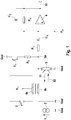
- FIG. 1 a schematic representation of a first exemplary embodiment is shown.
- a sound conversion device 5 is used for transmitting ultrasonic signals 11 and for receiving reflected ultrasonic signals 12.
- the ultrasonic signals 11 are preferably transmitted as pulses.
- the distance to the object at which the ultrasonic signal 11 has been reflected can be determined. This can be used inter alia in parking aids for vehicles. Due to the speed of sound of about 330 m / s results in a duration of about one ms for a distance of 15 cm of the sound transducer device to the object.
- the sound transducer device 5 can be formed by a pot diaphragm, which is moved by a piezo actuator.
- the piezoactuator corresponds to a good approximation in an electrical equivalent circuit diagram of a capacitor.
- the mechanical properties of the pot membrane such as their stiffness, mass and mechanical damping determine the resonant frequency and the decay of the transducer device. Their behavior can be modeled in the equivalent circuit diagram as a resistor, capacitor and inductance series circuit connected in parallel with the capacitor.
- the sound converter device 5 is connected in parallel to a secondary inductance 4b.
- the inductance 4b and the capacitance 5 of the sound transducer device 5 form in this way a parallel resonant circuit.
- the natural resonance of this parallel resonant circuit is adjusted so that it corresponds to the mechanical self-resonance of the sound transducer device 5. In this way, a maximum Deflection amplitude of the pot membrane achieved and thus generates a maximum sound pressure.
- the sound conversion device 5 is constructed such that their natural resonances are in the ultrasonic range.
- a signal 1 is coupled via a primary inductance 4a.
- the secondary and primary inductance may together form a transformer 4. This allows a voltage increase of the injected signal 1 from the primary side to the secondary side of the transformer 4.
- the signal 1 is provided by a current source 2, which via a switching element 3, e.g. a changeover switch, can be connected to the primary inductance 4a.
- the sound conversion device 5 converts the reflected ultrasonic signal 12 into a voltage signal. However, since only a small portion of the transmitted ultrasonic signal 11 is reflected, the corresponding voltage signal is very low. A typical magnitude of these voltage signals is in the range of a few microvolts.
- the signal amplitude in the parallel resonant circuit, which is used to excite the pot membrane, however, is in the range of 10 V - 200 V or greater.
- a purely mechanical damping of the pot membrane in order to achieve corresponding decay times is not desired, which precludes a high transmission sound pressure of the signal converter device 5.
- this attenuation would be permanent and also the reflected ultrasonic signals 12 attenuated by the mechanical damping.
- it is provided to attenuate the electrical parallel resonant circuit of the secondary inductance 4b and the capacitance of the sound transducer means 5 by attenuators R 1 and R 3 .
- These two attenuators R 1 , R 3 may have resistors.
- the attenuator R 3 forms with the switching device S 1 is a series circuit, which is connected in parallel to the secondary inductance 4 b.
- the parallel connection takes place via the ground potential Gnd. If the switching device S 1 is turned on , a current flows through the attenuator R 3 and a corresponding power is dissipated in the attenuator R 3 . With a suitable choice of the resistance of the attenuator R 3 , an attenuation of more than 140 dB can be achieved within a few ms.
- the switching device S 1 When receiving ultrasonic signals 12 through the sound transducer 5, the switching device S 1 is in a blocking state. In this case, the signal is attenuated solely by the current flow into the virtual ground via the resistor R 1 , which connects the sound transducer device 5 to the inverting input of the operational amplifier 6. This attenuation is advantageously kept small for receiving and transmitting ultrasonic signals by using a high resistance attenuator R 1 . Thus, the signals are only slightly attenuated. In the same way, a maximum sound pressure of the ultrasonic signal 11 can be achieved during transmission.
- the attenuator R 1 connects the parallel resonant circuit of the secondary inductance 4 b and the sound transducer device 5 with the inverting input of an operational amplifier 6.
- the operational amplifier 6 is fed back by means of a resistor R 2 and a capacitor C 2 . This allows received ultrasonic signals 12 and their corresponding voltage levels through the operational amplifier circuit from the operational amplifier 6, the attenuator R 1 , which now acts as a dropping resistor and amplify the feedback and output as an output signal 10.
- a further embodiment provides for using a noninverting operational amplifier circuit with a very high input resistance.
- the input of the operational amplifier is connected via a resistor to the ground potential and the parallel resonant circuit.
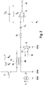
- FIG. 2 a second exemplary embodiment is shown.
- a series connection is made an attenuator R 4 and a switching device S 2 connected in parallel to the primary inductance 4a.
- the switching device S 2 In the conducting state of the switching device S 2 is in the attenuator R 4 (in the drawing falsely also R 2 instead of R4!) Dissipated power, which is the parallel resonant circuit of the secondary inductance 4 b and the sound transducer device 5 is removed.
- the transmission ratio N of the transformer 4 consisting of the primary inductance 4a and the secondary inductance 4b is taken into account. This results in a factor of 1 / N 2 .
- a first transistor T 1 is connected to the collector with a first voltage potential V 3 , which may be, for example, the supply voltage potential V DD of the operational amplifier 6.
- the transistor T 1 is of a first conductivity type.
- the transistor T 1 may be a bipolar or a field effect transistor.
- a transistor T 2 of a second conductivity type is connected with its collector to a second ground potential Gnd B , with which a supply line of the operational amplifier 6 may be connected.
- the emitters of the two transistors T 1 and T 2 are both connected to an inverting input of the operational amplifier 6.
- the transistor T 2 turns on and connects the inverting input of the transistor T 2 Operational amplifier 6 with the second ground potential Gnd B.
- the transistor T 1 turns on when the potential of an inverting the operational amplifier 6 by at least one threshold voltage of the transistor T 1 is less than the potential applied to the base of the transistor T 1 . In this case, the inverting input of the operational amplifier 6 is connected to the first voltage potential V 3 .
- the minimum amount of voltage thus required for a current to flow through the attenuator R 1 to the ground potential Gnd B and the first supply potential V 3 , respectively, may be controlled by the threshold voltage of the transistors and the potential at the base of the two transistors T 1 or T 2 is present.
- the two bases of the transistors are connected to the output signal of the feedback operational amplifier 6.
- there is a base of the transistors amplified inverted input signal which is applied to the inverting input of the operational amplifier 6.
- a signal of 50 mV at the inverting input of the operational amplifier and an exemplary gain of 10 thus results in a base potential of -500 mV at the transistor T 2 .
- the transistor T 2 switches to the conductive state.
- the transistor T 1 switches to the conducting state. It follows that from a voltage amplitude 50 mV, a current flows through the attenuator R 1 and then the parallel resonant circuit with the secondary inductance 4b and the sound transducer device 5 is attenuated. For voltage amplitudes which are less than 50 mV, attenuation is achieved by the feedback by the operational amplifier 6. In this case, the inverting input of the operational amplifier 6 can be regarded as a virtual ground.
- a switching device S 3 may be arranged. This allows the damping on or off.
- the DC potential of the operational amplifier 6 is decoupled from the DC potential of the parallel resonant circuit by a capacitor C 1 .
- a node 52 of a voltage divider of two resistors R 6 and R 7 is connected to the base of the transistors T 1 and T 2 .
- the voltage divider connects the supply voltage V 3 to the ground potential Gnd B.
- the resistors R 6 and R 7 are chosen to be the same size.
- a second voltage divider is formed by a resistor R 5 with the resistors R 6 and R 7 .
- This second voltage divider allows adaptation of the output signals of the operational amplifier 6, regardless of the selected gain of the operational amplifier circuit consisting of the input resistor R 1 , the feedback resistor R 2 and the operational amplifier. 6
- FIG. 4 is a schematic representation of a switching device for one of the embodiments shown.
- the switching device consists of two antiparallel arranged interconnected on both sides signal paths.
- a signal path has a diode, a transistor, z. B. on a field effect transistor.
- An external control signal V St can be applied to the field effect transistor.
- the first signal path for a second half-wave of the second signal path is turned on when a corresponding control signal V St is applied to the two transistors T 10 and T 11 .
- the diodes D 10 , D 11 can be omitted if the transistors have no internal protection diodes D 12 , D 13 .
- FIG. 5 a third exemplary embodiment is shown schematically.
- Parallel to the secondary inductance 4b is a series circuit of an attenuator R 1 and parallel circuit of two antiparallel connected diodes D 1 and D 2 is connected.
- the two diodes D 1 and D 2 are Schottky diodes. Since these have a very low threshold voltage of typically 0.2 volts, there is an attenuation of the parallel resonant circuit for signal amplitudes which are greater than 0.2 V. An attenuation for signal amplitudes which are less than 0.2 V can be achieved by the inverting input of the feedback operational amplifier 6.
Landscapes
- Engineering & Computer Science (AREA)
- Mechanical Engineering (AREA)
- Computer Networks & Wireless Communication (AREA)
- Physics & Mathematics (AREA)
- General Physics & Mathematics (AREA)
- Radar, Positioning & Navigation (AREA)
- Remote Sensing (AREA)
- Amplifiers (AREA)
- Filters And Equalizers (AREA)
- Measurement Of Velocity Or Position Using Acoustic Or Ultrasonic Waves (AREA)
Claims (12)
- Ensemble d'amortissement d'un circuit oscillant parallèle,
l'ensemble présentant un circuit oscillant parallèle doté d'une inductance secondaire (4b) et d'une première capacité (5),
un signal (1) pouvant être injecté par induction dans l'inductance secondaire (4b) par l'intermédiaire d'une inductance primaire (4a),
un organe d'amortissement (R1) présentant un circuit (S4) étant raccordé en parallèle à l'inductance secondaire,
caractérisé en ce que
un point de combinaison (51) entre le circuit oscillant parallèle et le circuit (S4) est relié à une entrée inversante d'un amplificateur opérationnel (6),
en ce qu'un premier transistor (T1) est disposé dans le circuit (S4) entre le point de combinaison (51) et un premier potentiel (V3) et un deuxième transistor (T2) est disposé entre le point de combinaison (51) et un premier potentiel de masse (GndB) et
en ce que les entrées de commande des deux transistors (T1, T2) sont reliées à la sortie de signal de l'amplificateur opérationnel (6). - Ensemble selon la revendication 1, dans lequel le circuit (S4) peut être commuté au moyen d'un signal de commutation externe (VSt).
- Ensemble selon au moins l'une des revendications 1 ou 2, dans lequel l'inductance primaire (4a) est reliée à une source de courant (2) par l'intermédiaire d'un élément de commutation (3).
- Ensemble selon l'une des revendications précédentes, dans lequel le circuit oscillant parallèle est relié par l'intermédiaire de l'organe d'amortissement (R1) et d'un condensateur (C1) à une entrée inversante de l'amplificateur opérationnel (6).
- Ensemble selon l'une des revendications précédentes, dans lequel un autre circuit (S3) est disposé entre les entrées de commande des deux transistors (T1, T2) et la sortie de signal (54) de l'amplificateur opérationnel (6).
- Ensemble selon au moins l'une des revendications 1 à 4, dans lequel un diviseur de tension (R5, R6) est disposé entre les entrées de commande des deux transistors (T1, T2) et la sortie de signal (54) de l'amplificateur opérationnel (6).
- Ensemble selon au moins l'une des revendications précédentes, dans lequel la capacité (5) est la capacité d'un dispositif (5) de conversion acoustique.
- Ensemble selon au moins l'une des revendications précédentes, dans lequel l'autre circuit (S3) présente des transistors (T10, T11).
- Ensemble selon la revendication 1, dans lequel l'autre circuit (S3) présente un circuit passif (D1, D11).
- Ensemble selon la revendication 9, dans lequel le circuit passif (D10, D11) présente deux diodes raccordées en opposition et raccordées en série à l'organe d'amortissement (R1).
- Ensemble selon au moins l'une des revendications 9 ou 10, dans lequel l'organe d'amortissement (R1) présente une résistance (R1) et des diodes Schottky (D10, D11).
- Procédé d'amortissement d'un circuit oscillant parallèle (4b, 5) qui présente une inductance secondaire (4b) et une première capacité (5),
un signal (1) pouvant être injecté par induction dans l'inductance secondaire (4b) par l'intermédiaire d'une inductance primaire (4a),
un circuit série formé d'un organe d'amortissement (R1) et d'un circuit (S4) étant raccordé en parallèle à l'inductance primaire (4a) et/ou à l'inductance secondaire,
un point de combinaison (51) entre le circuit oscillant parallèle et le circuit (S4) étant relié à une entrée inversante d'un amplificateur opérationnel (6),
un premier transistor (T1) étant disposé dans le circuit (S4) entre le point de combinaison (51) et un premier potentiel (V3) et un deuxième transistor (T2) étant disposé entre le point de combinaison (51) et un premier potentiel de masse (GndB) et
les entrées de commande des deux transistors (T1, T2) étant reliées à la sortie de signal de l'amplificateur opérationnel (6),
le procédé présentant l'étape qui consiste à commuter le circuit (S4) à l'état conducteur lorsque le signal (1) doit être amorti.
Applications Claiming Priority (2)
| Application Number | Priority Date | Filing Date | Title |
|---|---|---|---|
| DE102004058665A DE102004058665A1 (de) | 2004-12-06 | 2004-12-06 | Vorrichtung und Verfahren zur Dämpfung eines Parallelschwingkreises |
| PCT/EP2005/055939 WO2006061305A2 (fr) | 2004-12-06 | 2005-11-14 | Procede et dispositif pour attenuer un circuit oscillant parallele |
Publications (2)
| Publication Number | Publication Date |
|---|---|
| EP1825711A2 EP1825711A2 (fr) | 2007-08-29 |
| EP1825711B1 true EP1825711B1 (fr) | 2018-06-20 |
Family
ID=36500079
Family Applications (1)
| Application Number | Title | Priority Date | Filing Date |
|---|---|---|---|
| EP05816094.6A Expired - Lifetime EP1825711B1 (fr) | 2004-12-06 | 2005-11-14 | Procede et dispositif pour attenuer un circuit oscillant parallele |
Country Status (5)
| Country | Link |
|---|---|
| US (1) | US8107322B2 (fr) |
| EP (1) | EP1825711B1 (fr) |
| CN (1) | CN101073287B (fr) |
| DE (1) | DE102004058665A1 (fr) |
| WO (1) | WO2006061305A2 (fr) |
Families Citing this family (15)
| Publication number | Priority date | Publication date | Assignee | Title |
|---|---|---|---|---|
| DE102004058665A1 (de) * | 2004-12-06 | 2006-06-14 | Robert Bosch Gmbh | Vorrichtung und Verfahren zur Dämpfung eines Parallelschwingkreises |
| DE102006054095A1 (de) * | 2006-11-16 | 2008-05-21 | Siemens Ag | Ultraschallsensor sowie Verfahren zum Betrieb eines Ultraschallsensors |
| DE102008001971A1 (de) * | 2008-05-26 | 2009-12-03 | Robert Bosch Gmbh | Verfahren zur Diagnose eines Lastabfalls |
| DE102008025128B3 (de) * | 2008-05-26 | 2010-01-14 | Continental Automotive Gmbh | Schaltungsanordnung mit einem Schallwandler und Parksensor |
| DE102011076117B4 (de) * | 2011-05-19 | 2021-10-14 | Robert Bosch Gmbh | Ultraschall-Messsystem und Verfahren zum Detektieren eines Hindernisses mittels Ultraschall |
| DE102012213712A1 (de) * | 2012-08-02 | 2014-02-06 | Robert Bosch Gmbh | Verfahren zum Betrieb eines Ultraschallwandlers |
| DE102013210236A1 (de) * | 2013-06-03 | 2014-12-04 | Robert Bosch Gmbh | Ultraschall Sende- und Empfangsvorrichtung |
| US9568597B2 (en) * | 2013-08-13 | 2017-02-14 | Microchip Technology Inc. | Ultrasound capacitive T/R switch device, circuit |
| DE102013021328A1 (de) * | 2013-12-17 | 2015-06-18 | Valeo Schalter Und Sensoren Gmbh | Ultraschallsensoreinrichtung für ein Kraftfahrzeug, Kraftfahrzeug und entsprechendes Verfahren |
| EP3015879B1 (fr) * | 2014-10-29 | 2017-11-29 | Siemens Aktiengesellschaft | Dispositif de mesure de distance par écho d'impulsion ultrasonore |
| US10120434B2 (en) * | 2016-05-13 | 2018-11-06 | Infineon Technologies Ag | Semiconductor device chip package with electronic switching using dedicated ground pin coupled to a virtual ground node |
| JP2019029740A (ja) * | 2017-07-27 | 2019-02-21 | アイシン精機株式会社 | 超音波振動子駆動装置 |
| JP6911614B2 (ja) * | 2017-07-27 | 2021-07-28 | 株式会社アイシン | 超音波振動子駆動装置 |
| US12205400B2 (en) * | 2022-06-14 | 2025-01-21 | Huike (Singapore) Holding Pte.Ltd. | Ultrasonic transceiver system and electronic device |
| WO2024011519A1 (fr) * | 2022-07-14 | 2024-01-18 | 深圳市汇顶科技股份有限公司 | Appareil de détection d'empreintes digitales ultrasonore et équipement électronique |
Citations (2)
| Publication number | Priority date | Publication date | Assignee | Title |
|---|---|---|---|---|
| US5199299A (en) * | 1991-03-11 | 1993-04-06 | Iowa State University Research Foundation, Inc. | Ultrasonic unipolar pulse/echo instrument |
| US5267219A (en) * | 1992-07-17 | 1993-11-30 | Milltronics Ltd. | Acoustic range-finding system |
Family Cites Families (2)
| Publication number | Priority date | Publication date | Assignee | Title |
|---|---|---|---|---|
| US5070485A (en) * | 1990-09-28 | 1991-12-03 | Mts Systems Corporation | Low power magnetostrictive sensor |
| DE102004058665A1 (de) * | 2004-12-06 | 2006-06-14 | Robert Bosch Gmbh | Vorrichtung und Verfahren zur Dämpfung eines Parallelschwingkreises |
-
2004
- 2004-12-06 DE DE102004058665A patent/DE102004058665A1/de not_active Withdrawn
-
2005
- 2005-11-14 EP EP05816094.6A patent/EP1825711B1/fr not_active Expired - Lifetime
- 2005-11-14 US US11/792,600 patent/US8107322B2/en not_active Expired - Fee Related
- 2005-11-14 CN CN2005800417305A patent/CN101073287B/zh not_active Expired - Fee Related
- 2005-11-14 WO PCT/EP2005/055939 patent/WO2006061305A2/fr not_active Ceased
Patent Citations (2)
| Publication number | Priority date | Publication date | Assignee | Title |
|---|---|---|---|---|
| US5199299A (en) * | 1991-03-11 | 1993-04-06 | Iowa State University Research Foundation, Inc. | Ultrasonic unipolar pulse/echo instrument |
| US5267219A (en) * | 1992-07-17 | 1993-11-30 | Milltronics Ltd. | Acoustic range-finding system |
Also Published As
| Publication number | Publication date |
|---|---|
| WO2006061305A3 (fr) | 2006-12-07 |
| DE102004058665A1 (de) | 2006-06-14 |
| CN101073287B (zh) | 2012-11-28 |
| US8107322B2 (en) | 2012-01-31 |
| CN101073287A (zh) | 2007-11-14 |
| EP1825711A2 (fr) | 2007-08-29 |
| WO2006061305A2 (fr) | 2006-06-15 |
| US20110102114A1 (en) | 2011-05-05 |
Similar Documents
| Publication | Publication Date | Title |
|---|---|---|
| EP1825711B1 (fr) | Procede et dispositif pour attenuer un circuit oscillant parallele | |
| EP2984503B1 (fr) | Procédé de mesure par ultrason, notamment comme aide au stationnement pour véhicules, et systèmes de mesure par ultrason | |
| DE68925902T2 (de) | Stromquelle für eine wechselnde last mit einer induktiven last | |
| EP2780125B1 (fr) | Transducteur ultrasonique et dispositif correspondant de surveillance de l'environnement d'un véhicule | |
| DE10136628A1 (de) | Verfahren zum Betrieb eines Ultraschallwandlers zum Aussenden und Empfangen von Ultraschallwellen mittels einer Membran | |
| WO2017140673A1 (fr) | Système de mesure à ultrasons, en particulier pour la mesure de distances et/ou comme aide au stationnement pour des véhicules | |
| DE19836997B4 (de) | Sende/Empfangs-Schaltkreis und Sende/Empfangs-Verfahren für einen Wandler | |
| EP0738883B1 (fr) | Transducteur à ultrason intégré avec un amplificateur réglable | |
| DE10023306C2 (de) | Verfahren zur Ansteuerung von piezoelektrischen Antrieben in Füllstandmessgeräten | |
| DE3414423A1 (de) | Akustisches entfernungsmesssystem | |
| EP0623395B1 (fr) | Circuit pour amortir un transducteur d'ultrasons | |
| EP2880463B1 (fr) | Procédé seervant à faire fonctionner un transducteur ultrasonore | |
| EP3004919B1 (fr) | Dispositif émetteur-récepteur d'ultrasons | |
| DE102009000719B4 (de) | Elektrische Bedämpfung eines mechanisch schwingenden Bauteils | |
| DE10328113B4 (de) | Vorrichtung zum Betreiben einer schwingfähigen Einheit eines Vibrationsresonators | |
| DE19514330A1 (de) | Duplexer für ein Ultraschallabbildungssystem | |
| EP2692451B1 (fr) | Circuit électrique pour le fonctionnement d'une unité émettrice-réceptrice | |
| DE10018650C2 (de) | Auswerteschaltung für einen Sensor | |
| DE102006054605A1 (de) | Abstandsmessverfahren und Abstandsmessvorrichtung | |
| DE19721835C2 (de) | Schaltungsanordnung zum Betreiben eines Abstandssensors, insbesondere eines Ultraschallsensors | |
| DE2811668C2 (de) | Anpassungsschaltung für hochohmige Spannungsquellen | |
| DE102011076117B4 (de) | Ultraschall-Messsystem und Verfahren zum Detektieren eines Hindernisses mittels Ultraschall | |
| DE102008025126B4 (de) | Verfahren und Vorrichtung zum Betreiben eines Schallwandlers und Parksensor | |
| EP2904424B1 (fr) | Suppression de l'oscillation d'un convertisseur pour la détection environnementale | |
| DE102012208849A1 (de) | Vorrichtung zur Unterdrückung von Schwebungen bei der aktiven Dämpfung von Ultraschallsensoren |
Legal Events
| Date | Code | Title | Description |
|---|---|---|---|
| PUAI | Public reference made under article 153(3) epc to a published international application that has entered the european phase |
Free format text: ORIGINAL CODE: 0009012 |
|
| 17P | Request for examination filed |
Effective date: 20070706 |
|
| AK | Designated contracting states |
Kind code of ref document: A2 Designated state(s): DE FR GB IT |
|
| DAX | Request for extension of the european patent (deleted) | ||
| RBV | Designated contracting states (corrected) |
Designated state(s): DE FR GB IT |
|
| 17Q | First examination report despatched |
Effective date: 20080527 |
|
| REG | Reference to a national code |
Ref country code: DE Ref legal event code: R079 Ref document number: 502005015850 Country of ref document: DE Free format text: PREVIOUS MAIN CLASS: H04R0003000000 Ipc: G01S0007524000 |
|
| GRAP | Despatch of communication of intention to grant a patent |
Free format text: ORIGINAL CODE: EPIDOSNIGR1 |
|
| RIC1 | Information provided on ipc code assigned before grant |
Ipc: H03J 5/24 20060101ALI20180125BHEP Ipc: B06B 1/02 20060101ALI20180125BHEP Ipc: H03J 3/20 20060101ALI20180125BHEP Ipc: G01S 7/524 20060101AFI20180125BHEP |
|
| INTG | Intention to grant announced |
Effective date: 20180223 |
|
| GRAS | Grant fee paid |
Free format text: ORIGINAL CODE: EPIDOSNIGR3 |
|
| GRAA | (expected) grant |
Free format text: ORIGINAL CODE: 0009210 |
|
| AK | Designated contracting states |
Kind code of ref document: B1 Designated state(s): DE FR GB IT |
|
| REG | Reference to a national code |
Ref country code: GB Ref legal event code: FG4D Free format text: NOT ENGLISH |
|
| REG | Reference to a national code |
Ref country code: DE Ref legal event code: R096 Ref document number: 502005015850 Country of ref document: DE |
|
| REG | Reference to a national code |
Ref country code: DE Ref legal event code: R097 Ref document number: 502005015850 Country of ref document: DE |
|
| PLBE | No opposition filed within time limit |
Free format text: ORIGINAL CODE: 0009261 |
|
| STAA | Information on the status of an ep patent application or granted ep patent |
Free format text: STATUS: NO OPPOSITION FILED WITHIN TIME LIMIT |
|
| 26N | No opposition filed |
Effective date: 20190321 |
|
| PGFP | Annual fee paid to national office [announced via postgrant information from national office to epo] |
Ref country code: FR Payment date: 20191121 Year of fee payment: 15 Ref country code: IT Payment date: 20191120 Year of fee payment: 15 |
|
| PGFP | Annual fee paid to national office [announced via postgrant information from national office to epo] |
Ref country code: GB Payment date: 20191126 Year of fee payment: 15 Ref country code: DE Payment date: 20200124 Year of fee payment: 15 |
|
| REG | Reference to a national code |
Ref country code: DE Ref legal event code: R119 Ref document number: 502005015850 Country of ref document: DE |
|
| GBPC | Gb: european patent ceased through non-payment of renewal fee |
Effective date: 20201114 |
|
| PG25 | Lapsed in a contracting state [announced via postgrant information from national office to epo] |
Ref country code: FR Free format text: LAPSE BECAUSE OF NON-PAYMENT OF DUE FEES Effective date: 20201130 Ref country code: IT Free format text: LAPSE BECAUSE OF NON-PAYMENT OF DUE FEES Effective date: 20201114 |
|
| PG25 | Lapsed in a contracting state [announced via postgrant information from national office to epo] |
Ref country code: DE Free format text: LAPSE BECAUSE OF NON-PAYMENT OF DUE FEES Effective date: 20210601 Ref country code: GB Free format text: LAPSE BECAUSE OF NON-PAYMENT OF DUE FEES Effective date: 20201114 |