EP1833038B1 - Flachbildschirmgerät und Verfahren zur Erzeugung von Datensignalen dafür - Google Patents
Flachbildschirmgerät und Verfahren zur Erzeugung von Datensignalen dafür Download PDFInfo
- Publication number
- EP1833038B1 EP1833038B1 EP07102424A EP07102424A EP1833038B1 EP 1833038 B1 EP1833038 B1 EP 1833038B1 EP 07102424 A EP07102424 A EP 07102424A EP 07102424 A EP07102424 A EP 07102424A EP 1833038 B1 EP1833038 B1 EP 1833038B1
- Authority
- EP
- European Patent Office
- Prior art keywords
- signal
- voltage
- significant bits
- data signal
- video signal
- Prior art date
- Legal status (The legal status is an assumption and is not a legal conclusion. Google has not performed a legal analysis and makes no representation as to the accuracy of the status listed.)
- Not-in-force
Links
Images


Classifications
-
- G—PHYSICS
- G09—EDUCATION; CRYPTOGRAPHY; DISPLAY; ADVERTISING; SEALS
- G09G—ARRANGEMENTS OR CIRCUITS FOR CONTROL OF INDICATING DEVICES USING STATIC MEANS TO PRESENT VARIABLE INFORMATION
- G09G3/00—Control arrangements or circuits, of interest only in connection with visual indicators other than cathode-ray tubes
- G09G3/20—Control arrangements or circuits, of interest only in connection with visual indicators other than cathode-ray tubes for presentation of an assembly of a number of characters, e.g. a page, by composing the assembly by combination of individual elements arranged in a matrix no fixed position being assigned to or needed to be assigned to the individual characters or partial characters
- G09G3/2007—Display of intermediate tones
- G09G3/2077—Display of intermediate tones by a combination of two or more gradation control methods
- G09G3/2081—Display of intermediate tones by a combination of two or more gradation control methods with combination of amplitude modulation and time modulation
-
- G—PHYSICS
- G09—EDUCATION; CRYPTOGRAPHY; DISPLAY; ADVERTISING; SEALS
- G09G—ARRANGEMENTS OR CIRCUITS FOR CONTROL OF INDICATING DEVICES USING STATIC MEANS TO PRESENT VARIABLE INFORMATION
- G09G3/00—Control arrangements or circuits, of interest only in connection with visual indicators other than cathode-ray tubes
- G09G3/20—Control arrangements or circuits, of interest only in connection with visual indicators other than cathode-ray tubes for presentation of an assembly of a number of characters, e.g. a page, by composing the assembly by combination of individual elements arranged in a matrix no fixed position being assigned to or needed to be assigned to the individual characters or partial characters
- G09G3/22—Control arrangements or circuits, of interest only in connection with visual indicators other than cathode-ray tubes for presentation of an assembly of a number of characters, e.g. a page, by composing the assembly by combination of individual elements arranged in a matrix no fixed position being assigned to or needed to be assigned to the individual characters or partial characters using controlled light sources
-
- G—PHYSICS
- G09—EDUCATION; CRYPTOGRAPHY; DISPLAY; ADVERTISING; SEALS
- G09G—ARRANGEMENTS OR CIRCUITS FOR CONTROL OF INDICATING DEVICES USING STATIC MEANS TO PRESENT VARIABLE INFORMATION
- G09G3/00—Control arrangements or circuits, of interest only in connection with visual indicators other than cathode-ray tubes
- G09G3/20—Control arrangements or circuits, of interest only in connection with visual indicators other than cathode-ray tubes for presentation of an assembly of a number of characters, e.g. a page, by composing the assembly by combination of individual elements arranged in a matrix no fixed position being assigned to or needed to be assigned to the individual characters or partial characters
- G09G3/22—Control arrangements or circuits, of interest only in connection with visual indicators other than cathode-ray tubes for presentation of an assembly of a number of characters, e.g. a page, by composing the assembly by combination of individual elements arranged in a matrix no fixed position being assigned to or needed to be assigned to the individual characters or partial characters using controlled light sources
- G09G3/30—Control arrangements or circuits, of interest only in connection with visual indicators other than cathode-ray tubes for presentation of an assembly of a number of characters, e.g. a page, by composing the assembly by combination of individual elements arranged in a matrix no fixed position being assigned to or needed to be assigned to the individual characters or partial characters using controlled light sources using electroluminescent panels
-
- G—PHYSICS
- G09—EDUCATION; CRYPTOGRAPHY; DISPLAY; ADVERTISING; SEALS
- G09G—ARRANGEMENTS OR CIRCUITS FOR CONTROL OF INDICATING DEVICES USING STATIC MEANS TO PRESENT VARIABLE INFORMATION
- G09G3/00—Control arrangements or circuits, of interest only in connection with visual indicators other than cathode-ray tubes
- G09G3/20—Control arrangements or circuits, of interest only in connection with visual indicators other than cathode-ray tubes for presentation of an assembly of a number of characters, e.g. a page, by composing the assembly by combination of individual elements arranged in a matrix no fixed position being assigned to or needed to be assigned to the individual characters or partial characters
- G09G3/34—Control arrangements or circuits, of interest only in connection with visual indicators other than cathode-ray tubes for presentation of an assembly of a number of characters, e.g. a page, by composing the assembly by combination of individual elements arranged in a matrix no fixed position being assigned to or needed to be assigned to the individual characters or partial characters by control of light from an independent source
- G09G3/36—Control arrangements or circuits, of interest only in connection with visual indicators other than cathode-ray tubes for presentation of an assembly of a number of characters, e.g. a page, by composing the assembly by combination of individual elements arranged in a matrix no fixed position being assigned to or needed to be assigned to the individual characters or partial characters by control of light from an independent source using liquid crystals
-
- G—PHYSICS
- G09—EDUCATION; CRYPTOGRAPHY; DISPLAY; ADVERTISING; SEALS
- G09G—ARRANGEMENTS OR CIRCUITS FOR CONTROL OF INDICATING DEVICES USING STATIC MEANS TO PRESENT VARIABLE INFORMATION
- G09G2310/00—Command of the display device
- G09G2310/02—Addressing, scanning or driving the display screen or processing steps related thereto
- G09G2310/0243—Details of the generation of driving signals
- G09G2310/0259—Details of the generation of driving signals with use of an analog or digital ramp generator in the column driver or in the pixel circuit
-
- G—PHYSICS
- G09—EDUCATION; CRYPTOGRAPHY; DISPLAY; ADVERTISING; SEALS
- G09G—ARRANGEMENTS OR CIRCUITS FOR CONTROL OF INDICATING DEVICES USING STATIC MEANS TO PRESENT VARIABLE INFORMATION
- G09G2310/00—Command of the display device
- G09G2310/02—Addressing, scanning or driving the display screen or processing steps related thereto
- G09G2310/0264—Details of driving circuits
- G09G2310/0267—Details of drivers for scan electrodes, other than drivers for liquid crystal, plasma or OLED displays
-
- G—PHYSICS
- G09—EDUCATION; CRYPTOGRAPHY; DISPLAY; ADVERTISING; SEALS
- G09G—ARRANGEMENTS OR CIRCUITS FOR CONTROL OF INDICATING DEVICES USING STATIC MEANS TO PRESENT VARIABLE INFORMATION
- G09G2310/00—Command of the display device
- G09G2310/02—Addressing, scanning or driving the display screen or processing steps related thereto
- G09G2310/0264—Details of driving circuits
- G09G2310/0275—Details of drivers for data electrodes, other than drivers for liquid crystal, plasma or OLED displays, not related to handling digital grey scale data or to communication of data to the pixels by means of a current
-
- G—PHYSICS
- G09—EDUCATION; CRYPTOGRAPHY; DISPLAY; ADVERTISING; SEALS
- G09G—ARRANGEMENTS OR CIRCUITS FOR CONTROL OF INDICATING DEVICES USING STATIC MEANS TO PRESENT VARIABLE INFORMATION
- G09G2330/00—Aspects of power supply; Aspects of display protection and defect management
- G09G2330/02—Details of power systems and of start or stop of display operation
- G09G2330/021—Power management, e.g. power saving
Definitions
- the present invention relates to a flat panel display device and a data signal generating method thereof, and more particularly, to a flat panel display device and a data signal generating method thereof, in which the amplitude and the pulse width of a data signal are controlled to adjust a gray level of the data signal.
- a flat panel display device can be classified into an active matrix type and a passive matrix type according to its structure, and can also be classified into a memory driving type and a non-memory driving type according to its light emitting principle.
- the active matrix type is similar to the memory driving type
- the passive matrix type is similar to the non-memory driving type.
- the active matrix type and the memory driving type light is emitted per a unit of frame.
- the passive matrix type and the non-memory driving type the light is emitted per a unit of line.
- a passive matrix type flat panel display device is a display device in which horizontal lines are selected in sequence and uses a line scan method of emitting light only when the selected line of the horizontal lines is selected.
- the passive matrix type flat panel display device uses a pulse width modulation (PWM) method to control a pulse width of a data signal to adjust its brightness.
- PWM pulse width modulation
- FIG. 1 is a block diagram of a conventional data driver that generates a data signal based on a PWM method.
- the data driver includes a shift register 11, a latch 12; a counter 13, a comparator 14, a level shifter 15, and a buffer 16.
- the shift register 11 receives video signals in series and transmits the video signals to the latch 12.
- the latch 12 receives the video signals in series and outputs them in parallel to the comparator 14.
- the counter 13 uses clocks CLK to count numbers from '255' to '0' when the video signal has an input gray scale of 8 bits.
- the counter 13 either uses an up counter that counts in order of '0,' '1,' '2,' '3,' ..., '254,' '255,' or a down counter that counts in order of '255,' '254,' '253,' ...,' 1,' '0.'
- both the up counter and the down counter may be used as the counter 13.
- the down counter When both the up counter and the down counter are used, the down counter operates first and the up counter starts operating when the down counter finishes counting.
- the comparator 14 compares the number input from the latch 12 with the number counted by the counter 13, and outputs a signal when the value of the video signal corresponds (is coincident) with the value of the counter 13. In the case where the counter 13 employs both the up counter and the down counter, the comparator 14 first compares the number counted by the down counter with the value of the video signal and outputs a signal when they correspond (or are coincident) with each other. In the state that the signal output from the comparator 14 is maintained, the up counter starts counting when the down counter finishes counting.
- the comparator 14 compares the number counted by the up counter with the value of the video signal and stops outputting the signal when they correspond (or are coincident) with each other.
- the signal output from the comparator 14 is transmitted to the buffer 16 via the level shifter 15, thereby allowing the data signal to be generated.
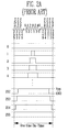
- FIGs. 2A , 2B , and 2C are timing diagrams illustrating PWM driving methods of the conventional data driver shown in FIG. 1 .
- FIG. 2A is a timing diagram of when the counter of the data driver uses both the down counter and the up counter
- FIG. 2B is a timing diagram of when the counter of the data driver uses only the down counter
- FIG. 2C is a timing diagram of when the counter of the data driver uses only the up counter.
- the data driver generates a data signal of representing a gray scale of 8 bits. During the time period that one line emits light (or one line on-time), the data driver controls an emission time of a pixel according to input gray levels of the video signals, thereby representing each of the gray levels.
- the data driver drives the down counter to count clocks from '255' to '0' and then the up counter to count clocks from '0' to '255'.
- the data driver controls the voltage of the data signal to have a ground voltage, thereby representing the gray level of '0.
- the data driver controls the voltage of the data signal to have a voltage Vpp between a time period when the down counter counts '1' and when the up counter counts '1.
- the data driver controls the voltage of the data signal to have the voltage Vpp between a time period when the down counter counts '255' and when the up counter counts '255.' Therefore, the time period for maintaining the data signal at the voltage Vpp is varied by the clocks of the counter according to gray levels.
- the data driver employs the down counter and the up counter to represent 255 gray levels. Also, the time period for maintaining the data signal at the voltage Vpp increases symmetrically with respect to the middle of the on time of one line (or one line on-time) as the gray level becomes higher.
- the foregoing PWM methods can be easily driven because of a linear relation between a pulse width and an emission current, but the power consumption in charging and discharging of electricity to apply an electric field between a gate electrode and a cathode electrode is high.
- the PWM methods represent the gray levels by dividing a relatively short time period for applying the scan signal.
- the gray level becomes higher, the on-time for applying the scan signal may be too short. That is, a gap between the gray levels may become so short that it becomes difficult to properly represent all the gray levels.
- the on-time corresponding to one line decreases, so that the time period that can be used to represent the gray levels is even more constrained as compared with the flat panel display device having a relatively low resolution.
- US 2004/0145597 A1 and US 6,590,581 B1 disclose driving methods for flat panel display devices where a frame is divided into a plurality of sub-fields which may have different periods and during each of which a driving voltage may be selected from a plurality of driving voltages.
- the claims have been characterised over US 2004/0145597 A1 .
- timing circuits which can produce a uniform grey scale in a PWM or a mixed PWM/amplitude driving scheme.
- a second aspect of the invention provides the flat panel display device as specified by claim 4, preferred embodiments of which are set forth in dependent claims 5 and 6.
- a third aspect of the invention provides a method of driving a flat panel display device is set forth in claims 7 and 8.
- FIG. 1 is a block diagram of a conventional data driver that generates a data signal based on a PWM method
- FIGs. 2A , 2B , and 2C are timing diagrams illustrating PWM driving methods of the conventional data driver shown in FIG. 1 ;
- FIG. 3 is a block diagram of a data driver according to an example useful for understanding the present invention.
- FIGs. 4A , 4B , 4C , 4D , 4E , and 4F are waveforms based on operations of the data driver according to the example;
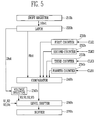
- FIG. 5 is a block diagram of a data driver according to an embodiment of the present invention.
- FIG. 6 is a waveform based on an operation of the data driver according to the embodiment of the present invention.
- FIG. 7 illustrates a flat panel display device employing the data driver according to an embodiment of the present invention.
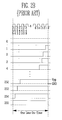
- FIG. 3 is a block diagram of a data driver according to an example useful for understanding the present invention.
- the data driver includes a shift register 210a, a latch 220a, a counter 230a, a comparator 240a, a voltage selector 250a, a level shifter 260a, and a buffer 270a.
- the shift register 210a receives a video signal of 10 bits for representing a gray level from '0' to '1023' in series, and transmits the video signal to the latch 220a.
- the latch 220a receives the video signal of 10 bits in series and outputs the video signal in parallel. In more detail, the latch 220a transmits the lower 8 bits of the video signal to the comparator 240a, and transmits the upper 2 bits of the video signal to the voltage selector 250a.
- the counter 230a includes an up counter and a down counter, or includes either the up counter or the down counter. The counter 230a counts clocks CLK.
- the comparator 240a compares a value of an input video signal with the number counted by the counter 230a, and then outputs a signal.
- the voltage selector 250a uses a signal of 2 bits to output a selection signal for selecting a voltage from among a total four voltages V0, V1, V2 and V3, but the present invention is not thereby limited.
- the level shifter 260a selects a low voltage from among the voltages V0, V1, V2 and V3, and a high voltage from among the voltages V1, V2, V3 and V4.
- the high voltage is the voltage V1.
- the high voltage is the voltage V2.
- voltage. V2 is selected as the low voltage
- the high voltage is the voltage V3.
- voltage V3 is selected as the low voltage
- the high voltage is the voltage V4.
- the level shifter 260a outputs a signal having a certain (or predetermined) voltage and a certain (or predetermined) on-time with the comparator 220a and the voltage selector 250a. Then, the signal output from the level shifter 260a is transmitted to the buffer 270a, thereby allowing the data signal to be output.
- FIGs. 4A through 4F are waveforms based on operation of the data driver according to the example.
- the data driver 200 receives a video signal of 10 bits, and represents a gray scale of 10 bits on the basis of the pulse width and the amplitude of a data signal.
- the counter 230 counts clocks while a scan driver 300 maintains one line in on-time.
- the counter 230 counts a rising time and a falling time of the clocks.
- the down counter first operates to count numbers from '255' to '0' in sequence, and the up counter then operates to count numbers from '0' to '255' in sequence.
- the voltage selector 250a outputs a selection signal to select (or outputs) a voltage from among four voltages as a reference (or low) voltage of the data signal.
- the voltage selector 250a selects the reference (or low) voltage from among the four voltages through the upper 2 bits of the input gray level of the video signal output from the latch 220.
- the upper 2 bits are 0 (10)
- the voltage V0 is selected as the reference voltage.
- the upper 2 bits are 1 (10) the voltage V1 is selected as the reference voltage.
- the voltage V2 is selected as the reference voltage.
- the upper 2 bits are 3 (10) the voltage V3 is selected as the reference voltage.
- the input video signal has a gray level of '0
- the upper 2 bits of the 10 bits are of 00 (2)
- the voltage V0 is selected as the low voltage of the data signal.
- the voltage V1 is selected as the high voltage of the data signal
- the lower 8 bits are of 00000000 (2) .
- the down counter operates to count from '255' to '0' and then the up counter operates to count from '0' to '255.'
- the signal compared by the comparator is '0', so that the data signal maintains the voltage V0 during an entire on-time of one line (or one line on-time).
- the input video signal has a gray level of '2
- the upper 2 bits among 10 bits are of 00 (2) , so that the voltage V0 is selected as the low voltage of the data signal.
- the voltage V1 is selected as the high voltage of the data signal, and the lower 8 bits are of 00000010 (2) .
- the down counter operates to count from '255' to '0' and then the up counter operates to count from '0' to '255.'
- the signal compared by the comparator is 2 (10) , so that the data signal maintains the voltage V0 until the down counter counts 2 (10) . Then, the data signal maintains the voltage V1 during the time period between when the down counter counts 2 (10) and when the up counter counts 2 (10) .
- the data signal After the up counter counts 2 (10) , the data signal returns to and maintains the voltage V0. Therefore, the data signal maintains the voltage V1 for a certain (or predetermined) time period with respect to the middle of the on-time of one line (or one line on-time or while the one line is in on-time), and maintains the voltage V0 for the rest of the time.
- the input video signal has a gray level of '258,' the upper 2 bits among 10 bits are of 01 (2) , so that the voltage V1 is selected as the low voltage of the data signal. Accordingly, the voltage V2 is selected as the high voltage of the data signal, and the lower 8 bits are of 00000010 (2) .
- the down counter operates to count from '255' to '0' and then the up counter operates to count from '0' to '255.'
- the signal compared by the comparator is 2 (10) , so that the data signal maintains the voltage V1 until the down counter counts 2 (10) . Then, the data signal maintains the voltage V2. during the time period between when the down counter counts 2 (10) and when the up counter counts 2 (10) .
- the data signal After the up counter counts 2 (10) , the data signal returns to and maintains the voltage V1. Therefore, the data signal maintains the voltage V2 for a certain (or predetermined) time period with respect to the middle of the on-time of one line, and maintains the voltage V1 for the rest of time.
- the upper 2 bits among 10 bits are of 10 (2) , so that the voltage V2 is selected as the low voltage of the data signal. Accordingly, the voltage V3 is selected as the high voltage of the data signal, and the lower 8 bits are of 00000010 (2) .
- the down counter operates to count from '255' to '0' and then the up counter operates to count from '0' to '255.'
- the signal compared by the comparator is 2 (10) , so that the data signal maintains the voltage V2 until the down counter counts 2 (10) . Then, the data signal maintains the voltage V3 during the time period between when the down counter counts 2 (10) and when the up counter counts 2 (10) .
- the data signal After the up counter counts 2 (10) , the data signal returns to and maintains the voltage V2. Therefore, the data signal maintains the voltage V2 for a certain (or predetermined) time period with respect to the middle of the on-time of one line, and maintains the voltage V2 for the rest of time.
- the input video signal has a gray level of '770
- the upper 2 bits among 10 bits are of 11 (2)
- the voltage V3 is selected as the low voltage of the data signal.
- the voltage V4 is selected as the high voltage of the data signal, and the lower 8 bits are of 0000001 0 (2) .
- the down counter operates to count from '255' to '0' and then the up counter operates to count from '0' to '255.
- the signal compared by the comparator is 2 (10) , so that the data signal maintains the voltage V3 until the down counter counts 2 (10) . Then, the data signal maintains a voltage V4 during the time period between when the down counter counts 2 (10) and when the up counter counts 2 (10) .
- the data signal After the up counter counts 2 (10) , the data signal returns to and maintains the voltage V3. Therefore, the data signal maintains the voltage V4 for a certain (or predetermined) time period with respect to the middle of the on-time of one line, and maintains the voltage V3 for the rest of time.
- the on-time of the video signal corresponding to one line should be longer than the counting time of the counter. If the on-time of one line is equal to the counting time of the counter, there is a problem that pairs of gray levels '255' and '256', '511' and '512', and '767' and '768' of the video signal may be represented as if they are the same.
- the gray level of '255' is represented by one time period (or section) for maintaining the voltage V1 and by another time period for maintaining the voltage V0, but the gray level of '256' is represented by only one time period (or section) for maintaining the voltage V1. Therefore, the gray levels of '255' and '256' can have a difference in brightness. Likewise, the gray levels of '511' and 512' and the gray levels of '767' and '768' can have differences in brightness.
- a reference voltage of a data signal of one example can be varied to correspond to the gray level of a video signal so that the amplitude of the data signal can also be varied according to the gray level of the video signal, thereby allowing the pulse width of the video signal represented by the gray scale higher than 8 bits to vary in a manner similar to a video signal represented by the gray scale of 8 bits. That is, even though data of the video signal has become larger to represent a larger (or higher) number of gray levels, relative difference in the pulse width of the data signal is not reduced for each of the gray levels.
- the difference in the pulse width is not reduced, there is no need to increase the amount of current in order to reduce or prevent a delay (or to improve a response characteristic of the data signals), thereby decreasing power consumption.
- FIG. 4B shows a negative driving waveform of when the counter includes both the up counter and the down counter.
- FIGs. 4C and 4D respectively show positive driving and the negative driving waveforms of when the counter includes only the down counter.
- FIGs. 4E and 4F respectively show positive driving and negative driving waveforms of when the counter includes only the up counter.
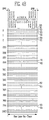
- FIG. 5 is a block diagram of a data driver according to an embodiment of the present invention.
- the data driver includes a shift register 210b, a latch 220b, first, second, third, and fourth counters 231 b, 232b, 233b and 234b, a comparator 240b, a voltage selector 250b, a level shifter 260b, and a buffer 270b.
- the shift register 210b receives a video signal of 10 bits in series, and transmits the video signal to the latch 220b.
- the latch 220b receives the video signal of 10 bits in series and outputs the video signal in parallel. In more detail, the latch 220b transmits the lower 8 bits of the video signal to the comparator 240b, and transmits the upper 2 bits of the video signal to the voltage selector 250b.
- Each of the first through fourth counters 231b, 232b, 233b and 234b includes an up counter and a down counter, or includes either the up counter or the down counter.
- Each of the first through fourth counters 231b, 232b, 233b and 234b counts clocks.
- One of the first through fourth counters 231 b, 232b, 233b and 234b is selected by the upper 2 bits of the video signal.
- the first through fourth counters 231 b, 232b, 233b and 234b respectively receive first clocks CLK1, second clocks CLK2. third clocks CLK3 and fourth clocks CLK4 and count them.
- the first clocks CLK1, the second clocks CLK2, the third clocks CLK3, and the fourth clocks CLK4 are different in a period from one another, so that times taken to count the same number are different. Accordingly, emission times between the gray levels corresponding to the amplitude of the data signal are differently set.
- the comparator 240b compares a value of an input video signal with the numbers counted by the first through fourth counters 231b, 232b, 233b and 234b, and then outputs a signal.
- the voltage selector 250b uses a signal of 2 bits in selecting a voltage. It is shown that the voltage selector 250b outputs a selection for selecting a voltage from among a total of four voltages V0, V1, V2 and V3 based on the signal of 2 bit, but the present invention is not thereby limited.
- the level shifter 260b selects a low voltage from among the voltages V0, V1, V2 and V3, and a high voltage from among the voltages V1, V2, V3 and V4.
- the high voltage is the voltage V1.
- the high voltage is the voltage V2.
- the voltage V2 is selected as the low voltage
- the high voltage is the voltage V3.
- the voltage V3 is selected as the low voltage
- the high voltage is the voltage V4.
- the level shifter 260b outputs a signal having a certain (or predetennined) voltage and a certain (or predetermined) on-time with the comparator 220b and the voltage selector 250b. Then, the signal output from the level shifter 260b is transmitted to the buffer 270b, thereby allowing the data signal to be output.
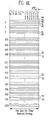
- FIG. 6 is a waveform based on operation of the data driver according to the embodiment of the present invention.
- the first through fourth clocks CLK1, CLK2, CLK3 and CLK4 different in a period from each other are input to the first through fourth counters 231b, 232b, 233b and 234b. Therefore, the emission time due to difference between the gray levels of the data signal is varied according to which one of the first through fourth clocks CLK1, CLK2, CLK3 and CLK4 is selected and respectively counted by the first through fourth counters 231b, 232b, 233b and 234b of the data driver.
- each of the first through fourth counters 231b, 232b, 233b and 234b includes only the down counter, but the present invention is not thereby limited.
- each of the first through fourth counters 231b, 232b, 233b and 234b may include the up counter, or may include both the up counter and the down counter.
- the first counter 231b receiving the first clock CLK1 is selected.
- the second counter 232b receiving the second clock CLK2 is selected.
- the third counter 233b receiving the third clock CLK3 is selected.
- the fourth counter 234b receiving the fourth clock CLK4 is selected.
- representing the gray level of the data signal is divided into a step of representing the gray levels from '0' to '255,' a step of representing the gray levels from '256' to '511,' a step of representing the gray levels from '512' to '767,' and a step of representing the gray levels from '768' to '1023.
- the times taken for the first through fourth counters 231b, 232b, 233b and 234b to count the same number are different from each other by the respective periods of the first through fourth clocks CLK1, CLK2, CLK3 and CLK4, so that the emission time corresponding to one gray level difference is varied according to which one of the first through fourth counters 231b, 232b, 233b and 234b operates.
- the emission time corresponding to one gray level difference can be further varied by the various steps of representing the gray level of the data signal.
- the on-time of the video signal corresponding to one line should be longer than the counting time of the counter. The reason for this was described above with reference to FIGs. 4A through 4F .
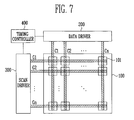
- FIG. 7 illustrates a flat panel display device employing the data driver according to an embodiment of the present invention.
- an electron emission display device is shown as an example of the flat panel display device, but the present invention is not thereby limited.
- the flat panel display device may be a plasma display panel.
- the electron emission display includes a display region 100, the data driver 200, a scan driver 300 and a timing controller 400.
- the display region 100 includes a plurality of pixels 101 in regions around where a plurality of cathode electrodes C1, C2, ..., Cn cross (or intersect) a plurality of gate electrodes G1, G2, ..., Gn.
- Each of the pixels 101 includes an electron emitting device.
- the electron emitting device emits electrons toward an anode, so that the electrons collide with the anode, thereby allowing a fluorescent material of the anode to emit light.
- an image is displayed.
- the gray level of the displayed image is varied according to values of input digital video signals.
- the gray levels according to the values of the digital video signals can be represented by a method of using differences in emission times based on a PWM method, and a method of using differences in the voltages between the cathode electrodes C1, C2, ..., Cn and the gate electrodes G1, G2, ..., Gn by adjusting a voltage of the data signal.
- the gray levels of the video signals are divided into a plurality of ranges, and the differences in voltages between the cathode electrodes C1, C2, ..., Cn and the gate electrodes G1, G2, ..., Gn are adjusted according to the ranges of the gray levels.
- the data driver 200 generates a data signal based on a video signal and is connected with the cathode electrodes C1, C2, ..., Cn, so that the data signal can be supplied to the display region 100.
- the display region 100 emits light based on the data signal.
- the data signal generated by the data driver 200 can have a plurality of voltage levels corresponding to the gray level of the video signal, and the gray level of the video signal can be categorized into the plurality of ranges, thereby allowing the data signal to have a voltage level that can be varied according to one or more of the ranges of the gray levels.
- the voltage applied to the cathode electrode C1, C2, ..., Cn is varied, so that the difference in the voltage between the cathode electrodes C1, C2, ..., Cn and the gate electrodes G1, G2,..., Gn is varied according to the one of the ranges of the gray levels, thereby causing brightness difference according to the ranges of the gray levels.
- each pixel of the electron emission display includes a parasitic capacitance (or capacitor). Therefore, power is consumed in charging and discharging the parasitic capacitance, thereby increasing the power consumption.
- the amount of the power consumed in charging and discharging the parasitic capacitance can be calculated by the following [Equation 1].
- P d n * m * C kg * V H 2 * F clk
- n is the number of row lines
- m is the number of column lines
- C kg is capacitance between the gate electrode and the cathode electrode
- V H is a voltage level of the data signal applied to the column lines
- F clk is a driving frequency of the data driver for the column lines.
- the voltage level V H is adjusted according to the ranges of the gray levels, so that it can have
- the power consumption does not increase even though the voltage level of the data signal becomes higher.
- the scan driver 300 is connected with the gate electrodes G1, G2, ..., Gn and supplies scan signals to the display region 100. Therefore, the scan driver 300 drives the display region 100 to emit light in sequence for a certain time per unit of a horizontal line based on a line scanning method, thereby displaying an image on an entire screen without increasing the production cost and the power consumption. Further, in one embodiment, the scan driver 300 applies (or leaves) a blank (or a blank signal) between a previous scan signal and a current scan signal so as to prevent the scan signals from overlapping due to the rising time and the falling time of each of the scan signals.
- the timing controller 400 transmits (or applies) a video signal, a data control signal, a scan control signal, etc. to the data driver 200 and the scan driver 300, and controls the data driver 200 and the scan driver 300 to operate, thereby allowing the display region 100 to display an image thereon.
- the present invention provides a flat panel display device and a data signal generating method thereof, in which a high gray level can be represented without reducing an emission time between the gray levels, so that the efficiency of representing the gray level is further enhanced, thereby improving a contrast. Further, additional electric current is not needed, thereby reducing a power consumption.
Landscapes
- Engineering & Computer Science (AREA)
- Physics & Mathematics (AREA)
- Computer Hardware Design (AREA)
- General Physics & Mathematics (AREA)
- Theoretical Computer Science (AREA)
- Chemical & Material Sciences (AREA)
- Crystallography & Structural Chemistry (AREA)
- Control Of Indicators Other Than Cathode Ray Tubes (AREA)
- Liquid Crystal (AREA)
- Transforming Electric Information Into Light Information (AREA)
Claims (8)
- Ein Datentreiber, umfassend:ein Schieberegister (210b), das dazu ausgelegt ist, ein Videosignal zu empfangen;einen Signalspeicher (220b), der dazu ausgelegt ist, höchstwertige Bits und niedrigstwertige Bits des Videosignals parallel auszugeben;einen Spannungswähler (250b), der dazu ausgelegt ist, ein Paar benachbarter Spannungspegel aus einer Vielzahl von Spannungspegeln (V0 - V4) als eine untere Spannung und eine obere Spannung für ein Datensignal zu selektieren, wobei die Selektion auf den höchstwertigen Bits des Videosignals basiert; undeinen Pegelumsetzer (260b), der dazu ausgelegt ist, gemäß einem Steuersignal entweder die untere Spannung oder die obere Spannung als das Datensignal an einen Anzeigebereich anzulegen;dadurch gekennzeichnet, dass er Folgendes umfasst:eine Vielzahl von Zählern (231b, 232b, 233b, 234b), die dazu ausgelegt sind, eine Anzahl an Taktereignissen zu zählen, wobei jeder der Zähler (231b, 232b, 233b, 234b) dazu ausgelegt ist, ein jeweiliges Taktsignal (CLK1 - CLK4) zu empfangen, wobei die Taktsignale sich in einer Periode voneinander unterscheiden, so dass die Zeiten, die die Zähler benötigen, um dieselbe Anzahl zu zählen, sich voneinander unterscheiden;Mittel, die dazu ausgelegt sind, einen der Zähler (231b, 232b, 233b, 234b), der den höchstwertigen Bits des Videosignals entspricht, zu selektieren;einen Komparator (240b), der dazu ausgelegt ist, die niedrigstwertigen Bits des Videosignals zu empfangen, dazu ausgelegt ist, die von dem selektierten der Zähler (231b, 232b, 233b, 234b) gezählte Anzahl mit den niedrigstwertigen Bits zu vergleichen, und dazu ausgelegt ist, das Steuersignal gemäß einem Ergebnis des Vergleichs auszugeben.
- Der Datentreiber nach Anspruch 1, wobei jeder der Vielzahl von Zählern (231b, 232b, 233b, 234b) dazu ausgelegt ist, innerhalb einer Zeilenperiode die den niedrigstwertigen Bits entsprechende Anzahl an Taktereignissen zu zählen.
- Der Datentreiber gemäß Anspruch 2, wobei die Zeilenperiode ein Zeitabschnitt ist, den mindestens einer der Zähler (231b, 232b, 233b, 234b) benötigt, um eine Anzahl an Taktereignissen zu zählen, die die den niedrigstwertigen Bits entsprechende Anzahl um mindestens eins übersteigt.
- Eine Flachbildschirmvorrichtung , umfassend:einen Anzeigebereich, der dazu ausgelegt ist, ein Datensignal und ein Abtastsignal zu empfangen, um ein Bild anzuzeigen;einen Datentreiber, der dazu ausgelegt ist, das Datensignal auf der Grundlage eines Videosignals zu erzeugen und das Datensignal an den Anzeigebereich zu liefern; undeinen Abtasttreiber, der dazu ausgelegt ist, das Abtastsignal zu erzeugen und das Abtastsignal an den Anzeigebereich zu liefern,wobei der Datentreiber dazu ausgelegt ist, einen Spannungspegel des Datensignals gemäß höchstwertigen Bits des Videosignals anzupassen und eine Pulsweite des Datensignals gemäß niedrigstwertigen Bits des Videosignals anzupassen, um die Helligkeit zu steuern,wobeider Datentreiber ein Datentreiber gemäß einem der vorhergehenden Ansprüche ist.
- Die Flachbildschirmvorrichtung gemäß Anspruch 4, wobei der Abtasttreiber dazu ausgelegt ist, ein Leersignal zwischen einem vorherigen Abtastsignal und einem aktuellen Abtastsignal einzufügen.
- Die Flachbildschirmvorrichtung gemäß einem der Ansprüche 4 oder 5, wobei die Flachbildschirmvorrichtung als Elektronenemissionsvorrichtung konfiguriert ist, die erste und zweite Substrate, die eine Vakuumhülle bilden, eine auf dem ersten Substrat vorgesehene Elektronenemissionseinheit und eine auf dem zweiten Substrat vorgesehene Lichtemissionseinheit umfasst.
- Ein Verfahren zum Erzeugen eines Datensignals auf der Grundlage eines eine Vielzahl von Graustufen repräsentierenden Videosignals, wobei das Verfahren Folgendes umfasst:Empfangen des Videosignals;Teilen des Videosignals in höchstwertige Bits und niedrigstwertige Bits;Selektieren eines Paares benachbarter Spannungspegel aus einer Vielzahl von Spannungspegeln (V0 - V4) als eine untere Spannung und eine obere Spannung für das Datensignal, wobei die Selektion auf den höchstwertigen Bits basiert;Bereitstellen entweder der unteren Spannung oder der oberen Spannung als das Datensignal gemäß einem Steuersignal;wobei das Verfahren dadurch gekennzeichnet ist, dass es Folgendes umfasst:Bereitstellen einer Vielzahl von Taktsignalen (CLK1 - CLK4);Zählen einer Anzahl an Taktereignissen mit einer Vielzahl von Zählern (231b - 234b), wobei jeder Zähler von einem verschiedenen der Vielzahl von Taktsignalen getaktet wird, wobei die Vielzahl von Taktsignalen (CLK1 - CLK4) sich in einer Periode voneinander unterscheiden, so dass die Zeiten, die die Zähler (231b - 234b) benötigen, um dieselbe Anzahl zu zählen, sich voneinander unterscheiden;Selektieren eines der Zähler gemäß den höchstwertigen Bits;Vergleichen der niedrigstwertigen Bits mit der gezählten Anzahl an Taktereignissen des selektierten Zählers; undErzeugen des Steuersignals gemäß einem Ergebnis des Vergleichs.
- Das Verfahren gemäß Anspruch 7, wobei die Pulsweite des Datensignals durch Zählen einer Anzahl an Taktereignissen in Folge in einem Zeitabschnitt bestimmt wird, der kürzer ist als eine Zeilenperiode.
Applications Claiming Priority (1)
| Application Number | Priority Date | Filing Date | Title |
|---|---|---|---|
| KR1020060022182A KR20070092856A (ko) | 2006-03-09 | 2006-03-09 | 평판표시장치 및 데이터신호 형성방법 |
Publications (2)
| Publication Number | Publication Date |
|---|---|
| EP1833038A1 EP1833038A1 (de) | 2007-09-12 |
| EP1833038B1 true EP1833038B1 (de) | 2009-09-16 |
Family
ID=37963647
Family Applications (1)
| Application Number | Title | Priority Date | Filing Date |
|---|---|---|---|
| EP07102424A Not-in-force EP1833038B1 (de) | 2006-03-09 | 2007-02-15 | Flachbildschirmgerät und Verfahren zur Erzeugung von Datensignalen dafür |
Country Status (6)
| Country | Link |
|---|---|
| US (1) | US20070211011A1 (de) |
| EP (1) | EP1833038B1 (de) |
| JP (1) | JP2007241228A (de) |
| KR (1) | KR20070092856A (de) |
| CN (1) | CN101034523A (de) |
| DE (1) | DE602007002425D1 (de) |
Families Citing this family (19)
| Publication number | Priority date | Publication date | Assignee | Title |
|---|---|---|---|---|
| KR101315373B1 (ko) | 2006-12-22 | 2013-10-08 | 삼성디스플레이 주식회사 | 액정 표시 장치 |
| KR100833755B1 (ko) * | 2007-01-15 | 2008-05-29 | 삼성에스디아이 주식회사 | 원장검사 장치 및 방법 |
| CN101393726B (zh) * | 2007-09-21 | 2011-02-02 | 北京京东方光电科技有限公司 | 像素灰度扩展方法、像素电容充电时间驱动方法及装置 |
| US20100321413A1 (en) * | 2009-06-23 | 2010-12-23 | Himax Technologies Limited | System and method for driving a liquid crystal display |
| US20100321412A1 (en) * | 2009-06-23 | 2010-12-23 | Himax Technologies Limited | System and method for driving a liquid crystal display |
| TWI421835B (zh) | 2010-05-10 | 2014-01-01 | Au Optronics Corp | 有機發光顯示器及其驅動方法 |
| CN101916533B (zh) * | 2010-05-19 | 2013-04-17 | 友达光电股份有限公司 | 有机发光显示器及其驱动方法 |
| CN102332247A (zh) * | 2011-11-25 | 2012-01-25 | 深圳市摩西尔电子有限公司 | 一种调节led灰度的方法 |
| CN102915705B (zh) * | 2012-11-17 | 2014-12-10 | 华北水利水电学院 | 一种提高带灰度led显示屏清晰度的时序发生电路 |
| KR102061554B1 (ko) | 2013-05-28 | 2020-01-03 | 삼성디스플레이 주식회사 | 표시 장치 및 그 구동 방법 |
| US20150317937A1 (en) * | 2014-05-04 | 2015-11-05 | Shenzhen China Star Optoelectronics Technology Co. Ltd. | Data driving circuit for driving liquid crystal panel and driving method of liquid crystal panel |
| KR20180002786A (ko) | 2015-06-05 | 2018-01-08 | 애플 인크. | 디스플레이 패널에 대한 방출 제어 장치들 및 방법들 |
| CN113345362B (zh) * | 2015-06-10 | 2024-02-02 | 苹果公司 | 显示面板冗余方案 |
| TWI557707B (zh) * | 2015-10-27 | 2016-11-11 | 國立交通大學 | 資料線驅動電路、資料線驅動器及顯示裝置 |
| US10297191B2 (en) | 2016-01-29 | 2019-05-21 | Samsung Display Co., Ltd. | Dynamic net power control for OLED and local dimming LCD displays |
| TWI622976B (zh) * | 2017-03-15 | 2018-05-01 | 明陽半導體股份有限公司 | 灰階產生電路與使用其之驅動電路 |
| US10861380B2 (en) * | 2018-05-14 | 2020-12-08 | Facebook Technologies, Llc | Display systems with hybrid emitter circuits |
| CN110310591B (zh) * | 2019-06-27 | 2024-07-05 | 富满微电子集团股份有限公司 | Led显示屏显示数据分割方法及系统 |
| EP4697315A3 (de) | 2020-01-06 | 2026-02-25 | Snap Inc. | Dynamische pixelmodulation |
Family Cites Families (15)
| Publication number | Priority date | Publication date | Assignee | Title |
|---|---|---|---|---|
| JP3367808B2 (ja) * | 1995-06-19 | 2003-01-20 | シャープ株式会社 | 表示パネルの駆動方法および装置 |
| JP2000056727A (ja) * | 1998-06-05 | 2000-02-25 | Matsushita Electric Ind Co Ltd | 表示パネルの階調駆動装置 |
| JP4646351B2 (ja) * | 1999-03-18 | 2011-03-09 | 株式会社半導体エネルギー研究所 | 表示装置 |
| US6590581B1 (en) | 1999-05-07 | 2003-07-08 | Semiconductor Energy Laboratory Co., Ltd. | Display device |
| JP2001350442A (ja) * | 1999-10-04 | 2001-12-21 | Matsushita Electric Ind Co Ltd | 表示パネルの駆動方法、表示パネルの輝度補正装置及び駆動装置 |
| US6894665B1 (en) * | 2000-07-20 | 2005-05-17 | Micron Technology, Inc. | Driver circuit and matrix type display device using driver circuit |
| JP2002311885A (ja) * | 2001-04-13 | 2002-10-25 | Canon Inc | 画像表示装置の駆動回路、画像表示装置、画像表示装置の駆動方法 |
| JP4566459B2 (ja) * | 2001-06-07 | 2010-10-20 | 株式会社日立製作所 | 表示装置 |
| TW552573B (en) * | 2001-08-21 | 2003-09-11 | Samsung Electronics Co Ltd | Liquid crystal display and driving method thereof |
| JP3911141B2 (ja) * | 2001-09-18 | 2007-05-09 | 株式会社日立製作所 | 液晶表示装置およびその駆動方法 |
| JP3851800B2 (ja) * | 2001-10-04 | 2006-11-29 | 株式会社東芝 | 電子ビーム発生装置 |
| JP2004233522A (ja) | 2003-01-29 | 2004-08-19 | Seiko Epson Corp | 電気光学装置の駆動方法、電気光学装置および電子機器 |
| JP4012118B2 (ja) * | 2003-05-19 | 2007-11-21 | キヤノン株式会社 | 画像表示装置 |
| KR100698983B1 (ko) * | 2004-03-30 | 2007-03-26 | 샤프 가부시키가이샤 | 표시 장치 및 구동 장치 |
| JP2006251453A (ja) * | 2005-03-11 | 2006-09-21 | Sanyo Electric Co Ltd | アクティブマトリクス型表示装置及びその駆動方法 |
-
2006
- 2006-03-09 KR KR1020060022182A patent/KR20070092856A/ko not_active Withdrawn
- 2006-07-13 JP JP2006193284A patent/JP2007241228A/ja active Pending
-
2007
- 2007-01-19 CN CNA2007100042593A patent/CN101034523A/zh active Pending
- 2007-02-15 EP EP07102424A patent/EP1833038B1/de not_active Not-in-force
- 2007-02-15 DE DE602007002425T patent/DE602007002425D1/de active Active
- 2007-03-01 US US11/681,119 patent/US20070211011A1/en not_active Abandoned
Non-Patent Citations (1)
| Title |
|---|
| P. PARRA, J. CASTRO, M. VALENCIA, A. J. ACOSTA: "Application of clock gating techniques at a flip-flop level to switching noise reduction in VLSI circuits", VLSI CIRCUITS AND SYSTEMS II, PROCEEDINGS OF SPIE, vol. 5837, June 2005 (2005-06-01), Bellingham, WA, 2005, pages 1003 - 1014 * |
Also Published As
| Publication number | Publication date |
|---|---|
| KR20070092856A (ko) | 2007-09-14 |
| JP2007241228A (ja) | 2007-09-20 |
| CN101034523A (zh) | 2007-09-12 |
| DE602007002425D1 (de) | 2009-10-29 |
| EP1833038A1 (de) | 2007-09-12 |
| US20070211011A1 (en) | 2007-09-13 |
Similar Documents
| Publication | Publication Date | Title |
|---|---|---|
| EP1833038B1 (de) | Flachbildschirmgerät und Verfahren zur Erzeugung von Datensignalen dafür | |
| US7358935B2 (en) | Display device of digital drive type | |
| US6784859B2 (en) | Plasma display drive method | |
| US7173580B2 (en) | Method for optimizing brightness in a display device and apparatus for implementing the method | |
| EP1333420A2 (de) | Steuerungsgerät für eine Flachanzeigetafel | |
| JP4269133B2 (ja) | Ac型pdpの駆動装置および表示装置 | |
| US7679628B2 (en) | Controller and image display device | |
| US6621228B2 (en) | EL display apparatus | |
| US20060232507A1 (en) | Plasma display apparatus and method of driving the same | |
| EP1227461B1 (de) | Plasma-Anzeige und Verfahren zu ihrer Steuerung | |
| EP1437704A2 (de) | Verfahren und Vorrichtung zur Ansteuerung einer Anzeigetafel | |
| EP1717785A1 (de) | Vorrichtung und Verfahren zur Ansteuerung einer Elektronenemissionsvorrichtung | |
| US5739799A (en) | Method of memory-driving a DC gaseous discharge panel and circuitry therefor | |
| JP2011018012A (ja) | 画像表示装置の制御方法 | |
| EP2107547A2 (de) | Bildanzeigevorrichtung und Steuerverfahren dafür | |
| JP2003316312A (ja) | 発光素子の駆動方法 | |
| US7471050B2 (en) | Organic EL drive circuit and organic EL display device | |
| CN100530289C (zh) | 具有减小信号失真的电子发射显示器(eed)及驱动eed的方法 | |
| EP2079071B1 (de) | Plasmaanzeigevorrichtung und Verfahren zu ihrer Ansteuerung | |
| CN100444222C (zh) | 等离子显示屏数据驱动器、驱动方法和等离子显示设备 | |
| US7336245B2 (en) | Display for using pulse width modulation to represent brightness and gray scales | |
| EP1998311A2 (de) | Anzeigevorrichtung mit Flachbildschirm | |
| US20060139249A1 (en) | Electron emission display and a method of driving the electron emission display | |
| KR20090047222A (ko) | 플라즈마 디스플레이 패널의 구동 방법 및 그를 이용한플라즈마 디스플레이 장치 | |
| EP1806720A2 (de) | Plasmaanzeigevorrichtung und Verfahren zu ihrer Ansteuerung |
Legal Events
| Date | Code | Title | Description |
|---|---|---|---|
| PUAI | Public reference made under article 153(3) epc to a published international application that has entered the european phase |
Free format text: ORIGINAL CODE: 0009012 |
|
| 17P | Request for examination filed |
Effective date: 20070215 |
|
| AK | Designated contracting states |
Kind code of ref document: A1 Designated state(s): AT BE BG CH CY CZ DE DK EE ES FI FR GB GR HU IE IS IT LI LT LU LV MC NL PL PT RO SE SI SK TR |
|
| AX | Request for extension of the european patent |
Extension state: AL BA HR MK YU |
|
| 17Q | First examination report despatched |
Effective date: 20071115 |
|
| AKX | Designation fees paid |
Designated state(s): DE FR GB |
|
| GRAP | Despatch of communication of intention to grant a patent |
Free format text: ORIGINAL CODE: EPIDOSNIGR1 |
|
| GRAC | Information related to communication of intention to grant a patent modified |
Free format text: ORIGINAL CODE: EPIDOSCIGR1 |
|
| GRAS | Grant fee paid |
Free format text: ORIGINAL CODE: EPIDOSNIGR3 |
|
| GRAA | (expected) grant |
Free format text: ORIGINAL CODE: 0009210 |
|
| AK | Designated contracting states |
Kind code of ref document: B1 Designated state(s): DE FR GB |
|
| REG | Reference to a national code |
Ref country code: GB Ref legal event code: FG4D |
|
| REF | Corresponds to: |
Ref document number: 602007002425 Country of ref document: DE Date of ref document: 20091029 Kind code of ref document: P |
|
| PLBE | No opposition filed within time limit |
Free format text: ORIGINAL CODE: 0009261 |
|
| STAA | Information on the status of an ep patent application or granted ep patent |
Free format text: STATUS: NO OPPOSITION FILED WITHIN TIME LIMIT |
|
| 26N | No opposition filed |
Effective date: 20100617 |
|
| PGFP | Annual fee paid to national office [announced via postgrant information from national office to epo] |
Ref country code: DE Payment date: 20110208 Year of fee payment: 5 Ref country code: FR Payment date: 20110218 Year of fee payment: 5 |
|
| PGFP | Annual fee paid to national office [announced via postgrant information from national office to epo] |
Ref country code: GB Payment date: 20110209 Year of fee payment: 5 |
|
| GBPC | Gb: european patent ceased through non-payment of renewal fee |
Effective date: 20120215 |
|
| REG | Reference to a national code |
Ref country code: FR Ref legal event code: ST Effective date: 20121031 |
|
| REG | Reference to a national code |
Ref country code: DE Ref legal event code: R119 Ref document number: 602007002425 Country of ref document: DE Effective date: 20120901 |
|
| PG25 | Lapsed in a contracting state [announced via postgrant information from national office to epo] |
Ref country code: FR Free format text: LAPSE BECAUSE OF NON-PAYMENT OF DUE FEES Effective date: 20120229 Ref country code: GB Free format text: LAPSE BECAUSE OF NON-PAYMENT OF DUE FEES Effective date: 20120215 |
|
| PG25 | Lapsed in a contracting state [announced via postgrant information from national office to epo] |
Ref country code: DE Free format text: LAPSE BECAUSE OF NON-PAYMENT OF DUE FEES Effective date: 20120901 |