EP1833073A1 - Bildanzeigeeinrichtung - Google Patents
Bildanzeigeeinrichtung Download PDFInfo
- Publication number
- EP1833073A1 EP1833073A1 EP05816506A EP05816506A EP1833073A1 EP 1833073 A1 EP1833073 A1 EP 1833073A1 EP 05816506 A EP05816506 A EP 05816506A EP 05816506 A EP05816506 A EP 05816506A EP 1833073 A1 EP1833073 A1 EP 1833073A1
- Authority
- EP
- European Patent Office
- Prior art keywords
- metal
- voltage
- layer
- resistance
- layers
- Prior art date
- Legal status (The legal status is an assumption and is not a legal conclusion. Google has not performed a legal analysis and makes no representation as to the accuracy of the status listed.)
- Granted
Links
Images

Classifications
-
- H—ELECTRICITY
- H01—ELECTRIC ELEMENTS
- H01J—ELECTRIC DISCHARGE TUBES OR DISCHARGE LAMPS
- H01J31/00—Cathode ray tubes; Electron beam tubes
- H01J31/08—Cathode ray tubes; Electron beam tubes having a screen on or from which an image or pattern is formed, picked up, converted, or stored
- H01J31/10—Image or pattern display tubes, i.e. having electrical input and optical output; Flying-spot tubes for scanning purposes
- H01J31/12—Image or pattern display tubes, i.e. having electrical input and optical output; Flying-spot tubes for scanning purposes with luminescent screen
- H01J31/123—Flat display tubes
- H01J31/125—Flat display tubes provided with control means permitting the electron beam to reach selected parts of the screen, e.g. digital selection
- H01J31/127—Flat display tubes provided with control means permitting the electron beam to reach selected parts of the screen, e.g. digital selection using large area or array sources, i.e. essentially a source for each pixel group
-
- H—ELECTRICITY
- H01—ELECTRIC ELEMENTS
- H01J—ELECTRIC DISCHARGE TUBES OR DISCHARGE LAMPS
- H01J2329/00—Electron emission display panels, e.g. field emission display panels
- H01J2329/18—Luminescent screens
- H01J2329/28—Luminescent screens with protective, conductive or reflective layers
Definitions
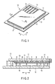
- An FED has a front substrate and a rear substrate, which are opposed to each other and spaced apart by a narrow gap of about 1 to 2 mm. These substrates are fused at their peripheral edges, with a rectangular frame-shaped side wall interposed between them. The substrates therefore form a vacuum envelope. The interior of the vacuum envelope is maintained at a high vacuum of about 10 -4 Pa. A plurality of spacers are provided between the substrates, supporting the substrates against the atmospheric pressure applied to them.
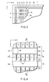
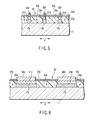
- getter-film segments 22a are formed, which are separated by gaps Gxg 20 ⁇ m wide in the X direction and by gaps Gyg 260 ⁇ m wide in the Y direction.
- FIG. 7 shows an equivalent circuit of the front substrate 11.
- the metal-back segments 20a arranged in the first direction X are connected by the first resistance-adjusting layers 31V.
- a resistor Rx and a capacitor Cx are formed between any adjacent metal-back segments 20a that are arranged in the first direction X.
- the metal-back segments 20a arranged in the second direction Y are connected by the second resistance-adjusting layers 31H.
- a resistor Ry and a capacitor Cy are formed between any adjacent metal-back segments 20a that are arranged in the second direction Y.
Landscapes
- Cathode-Ray Tubes And Fluorescent Screens For Display (AREA)
Applications Claiming Priority (2)
| Application Number | Priority Date | Filing Date | Title |
|---|---|---|---|
| JP2004376874A JP4750413B2 (ja) | 2004-12-27 | 2004-12-27 | 画像表示装置 |
| PCT/JP2005/023065 WO2006070612A1 (ja) | 2004-12-27 | 2005-12-15 | 画像表示装置 |
Publications (3)
| Publication Number | Publication Date |
|---|---|
| EP1833073A1 true EP1833073A1 (de) | 2007-09-12 |
| EP1833073A4 EP1833073A4 (de) | 2010-01-06 |
| EP1833073B1 EP1833073B1 (de) | 2010-11-03 |
Family
ID=36614732
Family Applications (1)
| Application Number | Title | Priority Date | Filing Date |
|---|---|---|---|
| EP05816506A Expired - Lifetime EP1833073B1 (de) | 2004-12-27 | 2005-12-15 | Bildanzeigeeinrichtung |
Country Status (6)
| Country | Link |
|---|---|
| US (1) | US7626325B2 (de) |
| EP (1) | EP1833073B1 (de) |
| JP (1) | JP4750413B2 (de) |
| DE (1) | DE602005024614D1 (de) |
| TW (1) | TWI291191B (de) |
| WO (1) | WO2006070612A1 (de) |
Cited By (2)
| Publication number | Priority date | Publication date | Assignee | Title |
|---|---|---|---|---|
| US8018133B2 (en) | 2006-12-25 | 2011-09-13 | Canon Kabushiki Kaisha | Image display apparatus |
| US8159122B2 (en) | 2007-12-20 | 2012-04-17 | Canon Kabushiki Kaisha | Light-emitting substrate and display apparatus using the same |
Families Citing this family (4)
| Publication number | Priority date | Publication date | Assignee | Title |
|---|---|---|---|---|
| TWI423665B (zh) * | 2006-10-10 | 2014-01-11 | Pentax Ricoh Imaging Co Ltd | 角速度偵測設備 |
| JP2008159449A (ja) * | 2006-12-25 | 2008-07-10 | Canon Inc | 表示装置 |
| JP2010015870A (ja) * | 2008-07-04 | 2010-01-21 | Canon Inc | 画像表示装置 |
| JP2011222439A (ja) * | 2010-04-14 | 2011-11-04 | Canon Inc | 画像表示装置 |
Family Cites Families (14)
| Publication number | Priority date | Publication date | Assignee | Title |
|---|---|---|---|---|
| FR2725072A1 (fr) * | 1994-09-28 | 1996-03-29 | Pixel Int Sa | Protection electrique d'une anode d'ecran plat de visualisation |
| JP3199682B2 (ja) | 1997-03-21 | 2001-08-20 | キヤノン株式会社 | 電子放出装置及びそれを用いた画像形成装置 |
| JP2000251797A (ja) | 1999-02-25 | 2000-09-14 | Canon Inc | 画像形成装置 |
| JP4304809B2 (ja) | 1999-03-05 | 2009-07-29 | ソニー株式会社 | 表示用パネル及びこれを用いた表示装置 |
| JP2003068237A (ja) | 2001-08-24 | 2003-03-07 | Toshiba Corp | 画像表示装置およびその製造方法 |
| JP4110912B2 (ja) * | 2002-05-24 | 2008-07-02 | ソニー株式会社 | 冷陰極電界電子放出表示装置 |
| JP4036078B2 (ja) * | 2002-11-05 | 2008-01-23 | ソニー株式会社 | 冷陰極電界電子放出表示装置 |
| JP2004273376A (ja) * | 2003-03-12 | 2004-09-30 | Sony Corp | 冷陰極電界電子放出表示装置 |
| JP2004335346A (ja) | 2003-05-09 | 2004-11-25 | Toshiba Corp | 画像表示装置 |
| JP4115403B2 (ja) * | 2004-02-18 | 2008-07-09 | キヤノン株式会社 | 発光体基板及び画像表示装置 |
| JP2005268109A (ja) * | 2004-03-19 | 2005-09-29 | Canon Inc | 発光体基板およびそれを用いた画像表示装置 |
| JP2006120622A (ja) * | 2004-09-21 | 2006-05-11 | Canon Inc | 発光スクリーン構造及び画像形成装置 |
| JP4027386B2 (ja) * | 2004-11-18 | 2007-12-26 | キヤノン株式会社 | 発光スクリーン構造及び画像形成装置 |
| JP4594076B2 (ja) * | 2004-12-27 | 2010-12-08 | キヤノン株式会社 | 画像表示装置 |
-
2004
- 2004-12-27 JP JP2004376874A patent/JP4750413B2/ja not_active Expired - Fee Related
-
2005
- 2005-12-15 DE DE602005024614T patent/DE602005024614D1/de not_active Expired - Lifetime
- 2005-12-15 EP EP05816506A patent/EP1833073B1/de not_active Expired - Lifetime
- 2005-12-15 WO PCT/JP2005/023065 patent/WO2006070612A1/ja not_active Ceased
- 2005-12-21 TW TW094145601A patent/TWI291191B/zh not_active IP Right Cessation
-
2007
- 2007-06-26 US US11/768,245 patent/US7626325B2/en not_active Expired - Fee Related
Cited By (3)
| Publication number | Priority date | Publication date | Assignee | Title |
|---|---|---|---|---|
| US8018133B2 (en) | 2006-12-25 | 2011-09-13 | Canon Kabushiki Kaisha | Image display apparatus |
| US8198799B2 (en) | 2006-12-25 | 2012-06-12 | Canon Kabushiki Kaisha | Image display apparatus |
| US8159122B2 (en) | 2007-12-20 | 2012-04-17 | Canon Kabushiki Kaisha | Light-emitting substrate and display apparatus using the same |
Also Published As
| Publication number | Publication date |
|---|---|
| DE602005024614D1 (de) | 2010-12-16 |
| TWI291191B (en) | 2007-12-11 |
| US20070246747A1 (en) | 2007-10-25 |
| EP1833073A4 (de) | 2010-01-06 |
| US7626325B2 (en) | 2009-12-01 |
| JP4750413B2 (ja) | 2011-08-17 |
| JP2006185701A (ja) | 2006-07-13 |
| WO2006070612A1 (ja) | 2006-07-06 |
| TW200629334A (en) | 2006-08-16 |
| EP1833073B1 (de) | 2010-11-03 |
Similar Documents
| Publication | Publication Date | Title |
|---|---|---|
| US7626325B2 (en) | Image display apparatus | |
| JP2005011700A (ja) | 画像表示装置 | |
| JP3971263B2 (ja) | 画像表示装置およびその製造方法 | |
| US7692370B2 (en) | Image display apparatus | |
| KR100761578B1 (ko) | 화상 표시 장치 | |
| EP1345250A2 (de) | Anzeige | |
| JP2005011701A (ja) | 画像表示装置 | |
| US20070228946A1 (en) | Image display device | |
| JP4551755B2 (ja) | 画像表示装置 | |
| EP1758148A1 (de) | Planare display-einrichtung | |
| JP2003109524A (ja) | 画像表示装置 | |
| US20070236131A1 (en) | Image display apparatus | |
| EP1732143A1 (de) | Bildanzeige | |
| JP2003100239A (ja) | 画像表示装置 | |
| EP1760757A1 (de) | Bildanzeigeeinrichtung und verfahren zu ihrer herstellung | |
| EP2249371B1 (de) | Lichtemittierendes Substrat mit lichtemittierenden Elementen und Bildanzeigevorrichtung mit dem lichtemittierenden Substrat | |
| US8253319B2 (en) | Light emitter substrate with improved withstand discharge characteristics, and image displaying apparatus using the same | |
| JP2008181867A (ja) | 画像表示装置 | |
| JP2008181857A (ja) | 画像表示装置、画像表示装置の製造方法、及び、機能付きフィルム | |
| EP1772891A1 (de) | Anzeigeeinheit | |
| WO2006011481A1 (ja) | 平面型表示装置 |
Legal Events
| Date | Code | Title | Description |
|---|---|---|---|
| PUAI | Public reference made under article 153(3) epc to a published international application that has entered the european phase |
Free format text: ORIGINAL CODE: 0009012 |
|
| 17P | Request for examination filed |
Effective date: 20070626 |
|
| AK | Designated contracting states |
Kind code of ref document: A1 Designated state(s): DE FR GB IT NL |
|
| DAX | Request for extension of the european patent (deleted) | ||
| RBV | Designated contracting states (corrected) |
Designated state(s): DE FR GB IT NL |
|
| RAP1 | Party data changed (applicant data changed or rights of an application transferred) |
Owner name: CANON KABUSHIKI KAISHA |
|
| A4 | Supplementary search report drawn up and despatched |
Effective date: 20091209 |
|
| 17Q | First examination report despatched |
Effective date: 20100330 |
|
| GRAP | Despatch of communication of intention to grant a patent |
Free format text: ORIGINAL CODE: EPIDOSNIGR1 |
|
| RIC1 | Information provided on ipc code assigned before grant |
Ipc: H01J 31/12 20060101AFI20100428BHEP Ipc: H01J 29/28 20060101ALI20100428BHEP |
|
| RIN1 | Information on inventor provided before grant (corrected) |
Inventor name: SUZUKI, KEIJIC/O INTELLECTUAL PROP. DIVISION, TOSH Inventor name: MURATA, HIROTAKAC/O INTELLECTUAL PROP. DIV., TOSH |
|
| GRAS | Grant fee paid |
Free format text: ORIGINAL CODE: EPIDOSNIGR3 |
|
| GRAA | (expected) grant |
Free format text: ORIGINAL CODE: 0009210 |
|
| AK | Designated contracting states |
Kind code of ref document: B1 Designated state(s): DE FR GB IT NL |
|
| REG | Reference to a national code |
Ref country code: GB Ref legal event code: FG4D |
|
| REF | Corresponds to: |
Ref document number: 602005024614 Country of ref document: DE Date of ref document: 20101216 Kind code of ref document: P |
|
| REG | Reference to a national code |
Ref country code: NL Ref legal event code: VDEP Effective date: 20101103 |
|
| PG25 | Lapsed in a contracting state [announced via postgrant information from national office to epo] |
Ref country code: NL Free format text: LAPSE BECAUSE OF FAILURE TO SUBMIT A TRANSLATION OF THE DESCRIPTION OR TO PAY THE FEE WITHIN THE PRESCRIBED TIME-LIMIT Effective date: 20101103 |
|
| PLBE | No opposition filed within time limit |
Free format text: ORIGINAL CODE: 0009261 |
|
| REG | Reference to a national code |
Ref country code: FR Ref legal event code: ST Effective date: 20110831 |
|
| STAA | Information on the status of an ep patent application or granted ep patent |
Free format text: STATUS: NO OPPOSITION FILED WITHIN TIME LIMIT |
|
| 26N | No opposition filed |
Effective date: 20110804 |
|
| PG25 | Lapsed in a contracting state [announced via postgrant information from national office to epo] |
Ref country code: FR Free format text: LAPSE BECAUSE OF NON-PAYMENT OF DUE FEES Effective date: 20110103 |
|
| REG | Reference to a national code |
Ref country code: DE Ref legal event code: R097 Ref document number: 602005024614 Country of ref document: DE Effective date: 20110804 |
|
| PG25 | Lapsed in a contracting state [announced via postgrant information from national office to epo] |
Ref country code: IT Free format text: LAPSE BECAUSE OF FAILURE TO SUBMIT A TRANSLATION OF THE DESCRIPTION OR TO PAY THE FEE WITHIN THE PRESCRIBED TIME-LIMIT Effective date: 20101103 |
|
| PGFP | Annual fee paid to national office [announced via postgrant information from national office to epo] |
Ref country code: GB Payment date: 20161230 Year of fee payment: 12 |
|
| PGFP | Annual fee paid to national office [announced via postgrant information from national office to epo] |
Ref country code: DE Payment date: 20161231 Year of fee payment: 12 |
|
| REG | Reference to a national code |
Ref country code: DE Ref legal event code: R119 Ref document number: 602005024614 Country of ref document: DE |
|
| GBPC | Gb: european patent ceased through non-payment of renewal fee |
Effective date: 20171215 |
|
| PG25 | Lapsed in a contracting state [announced via postgrant information from national office to epo] |
Ref country code: DE Free format text: LAPSE BECAUSE OF NON-PAYMENT OF DUE FEES Effective date: 20180703 |
|
| PG25 | Lapsed in a contracting state [announced via postgrant information from national office to epo] |
Ref country code: GB Free format text: LAPSE BECAUSE OF NON-PAYMENT OF DUE FEES Effective date: 20171215 |