EP1833175B1 - Anfangszellensuchalgorithmus - Google Patents
Anfangszellensuchalgorithmus Download PDFInfo
- Publication number
- EP1833175B1 EP1833175B1 EP07111143.9A EP07111143A EP1833175B1 EP 1833175 B1 EP1833175 B1 EP 1833175B1 EP 07111143 A EP07111143 A EP 07111143A EP 1833175 B1 EP1833175 B1 EP 1833175B1
- Authority
- EP
- European Patent Office
- Prior art keywords
- module
- offset
- controller
- scrambling code
- frequency
- Prior art date
- Legal status (The legal status is an assumption and is not a legal conclusion. Google has not performed a legal analysis and makes no representation as to the accuracy of the status listed.)
- Expired - Lifetime
Links
- 238000010845 search algorithm Methods 0.000 title description 11
- 238000000034 method Methods 0.000 claims description 27
- 239000000872 buffer Substances 0.000 claims description 23
- 238000004891 communication Methods 0.000 claims description 23
- 230000007717 exclusion Effects 0.000 claims description 18
- 239000013598 vector Substances 0.000 claims description 14
- 238000001514 detection method Methods 0.000 claims description 10
- 230000008569 process Effects 0.000 claims description 9
- 230000003044 adaptive effect Effects 0.000 claims description 2
- 239000011159 matrix material Substances 0.000 description 36
- 238000010586 diagram Methods 0.000 description 15
- 230000001427 coherent effect Effects 0.000 description 4
- 230000010354 integration Effects 0.000 description 4
- 230000003111 delayed effect Effects 0.000 description 3
- 238000012545 processing Methods 0.000 description 3
- 230000035508 accumulation Effects 0.000 description 2
- 238000009825 accumulation Methods 0.000 description 2
- 230000000875 corresponding effect Effects 0.000 description 2
- 125000004122 cyclic group Chemical group 0.000 description 2
- 239000000284 extract Substances 0.000 description 2
- 238000005259 measurement Methods 0.000 description 2
- 230000007480 spreading Effects 0.000 description 2
- 230000001360 synchronised effect Effects 0.000 description 2
- 101100129500 Caenorhabditis elegans max-2 gene Proteins 0.000 description 1
- 230000015556 catabolic process Effects 0.000 description 1
- 230000008859 change Effects 0.000 description 1
- 238000012937 correction Methods 0.000 description 1
- 230000002596 correlated effect Effects 0.000 description 1
- 230000006735 deficit Effects 0.000 description 1
- 238000006731 degradation reaction Methods 0.000 description 1
- 238000011156 evaluation Methods 0.000 description 1
- 238000010295 mobile communication Methods 0.000 description 1
- 239000003607 modifier Substances 0.000 description 1
- 230000004044 response Effects 0.000 description 1
- 238000012216 screening Methods 0.000 description 1
- 238000001228 spectrum Methods 0.000 description 1
- 238000010408 sweeping Methods 0.000 description 1
Images








Classifications
-
- H—ELECTRICITY
- H04—ELECTRIC COMMUNICATION TECHNIQUE
- H04W—WIRELESS COMMUNICATION NETWORKS
- H04W56/00—Synchronisation arrangements
-
- H—ELECTRICITY
- H04—ELECTRIC COMMUNICATION TECHNIQUE
- H04B—TRANSMISSION
- H04B1/00—Details of transmission systems, not covered by a single one of groups H04B3/00 - H04B13/00; Details of transmission systems not characterised by the medium used for transmission
- H04B1/69—Spread spectrum techniques
- H04B1/707—Spread spectrum techniques using direct sequence modulation
-
- H—ELECTRICITY
- H04—ELECTRIC COMMUNICATION TECHNIQUE
- H04B—TRANSMISSION
- H04B1/00—Details of transmission systems, not covered by a single one of groups H04B3/00 - H04B13/00; Details of transmission systems not characterised by the medium used for transmission
- H04B1/69—Spread spectrum techniques
- H04B1/707—Spread spectrum techniques using direct sequence modulation
- H04B1/7073—Synchronisation aspects
- H04B1/7083—Cell search, e.g. using a three-step approach
-
- H—ELECTRICITY
- H04—ELECTRIC COMMUNICATION TECHNIQUE
- H04J—MULTIPLEX COMMUNICATION
- H04J3/00—Time-division multiplex systems
- H04J3/02—Details
- H04J3/06—Synchronising arrangements
- H04J3/0602—Systems characterised by the synchronising information used
- H04J3/0605—Special codes used as synchronising signal
- H04J3/0608—Detectors therefor, e.g. correlators, state machines
-
- H—ELECTRICITY
- H04—ELECTRIC COMMUNICATION TECHNIQUE
- H04W—WIRELESS COMMUNICATION NETWORKS
- H04W48/00—Access restriction; Network selection; Access point selection
- H04W48/16—Discovering, processing access restriction or access information
-
- H—ELECTRICITY
- H04—ELECTRIC COMMUNICATION TECHNIQUE
- H04J—MULTIPLEX COMMUNICATION
- H04J11/00—Orthogonal multiplex systems, e.g. using WALSH codes
- H04J11/0069—Cell search, i.e. determining cell identity [cell-ID]
Definitions
- the transmit order of the SSC depends on the primary scrambling code group number. As an example, in a five hundred and twelve (512) cell system, there are sixty four (64) groups. In each group, the patterns of the SSC and its cyclic shifts are different. As a result, there are five hundred and twelve (512) primary scrambling codes. Each cell, of a five hundred and twelve cell (512) system, is assigned a code such that no one code is used by more than one cell in a given reception area.
- the cell search synchronization systems determine the primary scrambling code of a cell utilizing an initial cell search algorithm.
- Common initial cell search algorithms utilize three (3) major algorithms: a step 1 algorithm detects the PSC and determines a chip offset; a step 2 algorithm uses the information given by step 1 and detects the slot offset and code group number; and a step 3 algorithm utilizes the information provided by the step 2 algorithm and detects the primary scrambling code.
- each step algorithm has an inherent error associated with it. The error present in each of the steps is caused by the UE detection of noise associated with the received common downlink channel, which can result in a high number of false detections.
- the common initial cell search algorithms can not handle a rejection by the upper layers ofthe wrong public land mobile network (PLMN). Since most algorithms detect the strongest cell in the common downlink channel, it is likely that each time the algorithm locates a cell the same PLMN will be associated with the cell. This results in a deadlock and ultimately an indication to the UE that there is no service.
- PLMN public land mobile network
- a method for signal transmitting and spread-spectrum code synchronizing method for mobile communication system is disclosed.
- a mobile station first carries out correlation detection by a matched filter using a short code common to all the cells as a spreading code replica.
- the mobile station is then connected to the base station which has sent the signal associated with the maximum correlation peak.
- the mobile station carries out correlation detection between the received signal and the short code used as the spreading code replica to detect the phase of the received long code from the timing of the maximum peak.
- a user equipment shall scan all RF channels in the UTRA band according to its capabilities to find available public land mobile networks (PLMNs). On each carrier, the UE shall search for the strongest cell and read its system information. The UE may optimize the search by using stored information of carrier frequencies and optionally also information on cell parameters from previously received measurement control information elements.
- PLMNs public land mobile networks
- WO 00/31998 discloses a method for searching for the presence narrowband signals by first selecting a wider receiver bandwidth.
- WO01/01596 discloses a user equipment comprising the features of the preamble of claim 1 of the present application.
- the present invention is a system and method for conducting initial cell search and establishing a communication link between a UE and a base station in a communication network.
- the communication signal is first processed to generate an index value and chip offset associated with a primary synchronization code, producing a first decision.
- a peak sample of the communication signal is extracted and a second processing is conducted on the communication signal.
- the secondprocessing retrieves the code group number, slot offset, and secondary synchronization code from the communication signal, producing a second decision.
- a third processing is conducted on the communication signal in response to the code group number and slot offset, which retrieves the primary scrambling code.
- the primary scrambling code is then used for synchronizing the UE to the cell associated with the primary scrambling code.
- window exclusion logic is employed to enhance the screening of frequency bands while performing the initial code search.
- rejected chip offsets and rejected primary scrambling codes are stored for the purpose of checking and comparing by the window exclusion logic, which can then restart the decision process upon detection of a wrong PLMN, thereby avoiding a deadlock condition.
- the cell search synchronization system 10 in accordance with the preferred embodiment of the present invention is illustrated in Figure 1 .
- the system 10 comprises a step 1 module 12, a step 2 module 14, a step 3 module 16, and a controller 18 to accomplish synchronization between a user equipment (UE) and a base station.
- UE user equipment
- the UE through the cell search synchronization system 10, utilizes an initial cell search algorithm, to be disclosed hereinafter.
- the step 1 algorithm of the initial cell search algorithm is accomplished using the step 1 module 12.
- the step 1 module 12 comprises two Hierarchical Golay Correlators (HGC) 21, 22, two absolute value modifiers (AVM) 23,24, a decision circuit 25, a normalizer circuit 26, a look up table 27, a multiplier 28, a splitter 19, and a step 1 comparator 29.
- the root raised cosine filter (RRCFIR) 1 shown is not a part of the step 1 module 12, but are illustrated therein to provide a complete picture.
- the HGCs 21, 22 are coupled to the AVMs 23, 24, and the sample selector 34 of the step 2 module 14 (illustrated in Figure 5 ), to be disclosed hereinafter.
- HGCs 21, 22 correlate the PSC of the input signal.
- the HGCs 21, 22 output the complex values of the even and odd samples of the input signal, respectively.
- the HGC 21, 22 outputs are forwarded to the AVMs 23, 24 and the sample selector 34.
- the use ofthe approximated absolute value in accordance with Equation 1 reduces the hardware required in this implementation and causes no significant performance degradation.
- the accumulator when the first sample value of slot 1 is added to the first register value, the accumulator has the values ⁇ 1,0,0,0 ⁇ ; when the second sample value of slot 1 is added to the second register value, the accumulator has the values ⁇ 1,5,0,0 ⁇ and so on.
- the first sample value of slot 2 is added to the first register of the accumulator, resulting in the accumulator having the values ⁇ 3,5,3,7 ⁇ ; when the second sample value of slot 2 is added to the second register value, the accumulator has the values ⁇ 3,9,3,7 ⁇ .
- the preferred embodiment of the present invention flushes the registers of the accumulator after five (5) frames have been accumulated, which is equivalent to seventy five (75) slots.
- the number of accumulated frames is counted by a step 1 counter (not shown) within the decision circuit 25.
- the decision circuit 25 also comprises a mask generator 5, which is used to exclude a window around a rejected chip offset from detection by the decision circuit 25.
- This mask generator 5, therefore, prohibits the decision circuit 25 from utilizing an index associated with a rejected chip offset.
- the details of the mask generator 5 will be disclosed hereinafter.
- the calculated chip offset and the frame count step 1 counter are output to a controller 18, to be disclosed hereinafter.
- the decision circuit 25 also outputs the maximum accumulated chip value MAX and the accumulated chip value OUTPUT for all registers.
- the accumulated chip value OUTPUT for all registers is output to a normalizer circuit 26, where it is sampled at 20% the chip rate (one out of five), summed, and then normalized to 1024.
- the frame count step 1 counter is output to the lookup table 27 to determine the proper gain factor based on the number of frames accumulated.
- the output of the normalizer circuit 26 and the lookup table 27 are then multiplied by the multiplier 28.
- the output of the multiplier 28 is considered the Noise Threshold and is forwarded to a step 1 comparator circuit 29, to be compared to the maximum accumulated sample value MAX. If the maximum accumulated sample value MAX is greater than the Noise Threshold, the differential amplifier 29 outputs a high step1 firm signal to the controller, indicating a good decision for step 1, otherwise a low signal is output.
- the chip offset and other outputs are determined at the end of every frame. Therefore, the reliability of the first decision is less than that of the second because the second decision is made over thirty slots instead of fifteen slots. The reliability increases as the number of slots accumulated increases.
- the highest reliable output is generated at the M1th frame, M1 being an integer greater than or equal to one (1).
- the controller 18 resets the frame count step 1 counter and the accumulator registers at the end of every M1th frame.
- the performance results under different channel impairment show that five-frame integration is good enough to detect PSC. However, this integration can be changed to more or less frames.
- a flow diagram of the step 1 module is illustrated in Figure 4 .
- the UE detects the receipt of communications over the common downlink channel (step 401) and samples the signal at twice the chip rate generating even and odd samples (step 402). These even and odd samples are passed to the hierarchical Golay correlators (HGC) 21, 22 (step 403).
- the HGCs 21, 22 then forwards the outputs to the AVMs 23, 24 and sample selector 34 (step 404).
- the AVMs 23, 24 approximate the magnitudes of the even and odd outputs received from the HGCs 21,22 (step 405) and forwards them to the decision circuit 25 (step 406).
- the decision circuit 25 Upon receipt of the output magnitudes the decision circuit 25 combines the magnitudes (step 407), which represents the signal strength of the signal transmitted in one of the samples of each slot of each frame. The signal strength for each sample is accumulated for all slots within each frame (step 408). The decision circuit 25 then determines which sample in the frame has the maximum accumulated sample value (step 409) and assigns an index to it (step 410). Based on the index, a chip value is assigned to the index (step 411), known as the chip offset, and output to the controller 18 (step 412). A noise threshold value is then generated using the accumulated chip value for all samples and the frame count (step 413) and then compared to the maximum accumulated sample value (step 414), indicating a firm or tentative decision to the controller 18 (step 415).
- the outputs of the step 1 module 12, the chip offset, step 1 firm, and step 1 counter, are forwarded to the controller 18.
- the controller 18 forwards the chip offset to the step 2 module 14.
- the step 2 module 14 utilizes a step 2 algorithm which takes the chip offset output from step 1 and the HGC 21, 22 outputs and detects the slot offset and the code group number.
- the step 2 module 14 illustrated in Figure 5 comprises a step 2 comparator 30, a delay 32, a sample selector 34, a conjugator 36, a complex multiplier 38, a Fast Hadamard Transform (FHT) 3 3, an envelope remover 31, an input matrix generator 3 5, an RS encoder 37, and a step 2 decision circuit 39.
- FHT Fast Hadamard Transform
- the same communication signal to the step 1 module 12 is input to an alignment circuit 15, which aligns the input signal so that step 2 module 14 begins it search for the scrambling code group number and slot offset at the beginning of the slot.
- the alignment circuit 15 forwards it to the step 2 module 14. Even though there are two thousand five hundred and sixty (2,560) chips in each slot, it should be apparent from Figure 2 that the PSC is located within the first 256 chips of each slot. Since the chip offset has been determined by the step 1 module, the step 2 module determines the SSC using the location of the strongest PSC in the first 256 chips in each slot.
- the signal is output from the envelope remover 31 to the FHT transform 33 coupled to the envelope remove 31 and multiplier 38, which reduces the complexity of the pure Hadamard correlation operation.
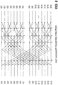
- Figure 6 is an illustration of the FHT structure.
- the output of the FHT transform 33 is multiplied by the conjugate of the peak HGC 21, 22 by the complex multiplier 38 coupled to the conjugator 36 and the FHT transform 33.
- the use of the conjugate of the peak output from the HGCs 21, 22 provides a phase correction to the FHT output and transforms the one entry that corresponds to the transmitted SSC code onto the real axis.
- a correlation matrix is generated within the step 2 decision circuit 39 using the input matrix 35 and a known code group matrix, which results in a 64 X 15 matrix.
- the correlation matrix is reset when the frame counter for the step 2 module reaches M2, similar to that disclosed in the step 1 module.
- the structure of the code group matrix and the resulting correlation matrix are illustrated in Figures 8 and 9 respectively.
- the comparator circuit 30 will output a high step 2 firm signal to the controller 18 indicating a firm decision, otherwise a low signal is output indicating a tentative decision.
- the step 2 module 14 outputs to the controller 18 the code group number, slot offset, step 2 firm, and step 2 counter.
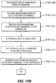
- the flow diagram for the step 2 algorithm is illustrated in Figure 10 .
- the step 2 module receives the communication signal from the base station over the downlink channel (step 1001).
- An envelope sequence is removed from the communication signal (step 1002a) and output to an FHT transform 33, (step 1003a).
- the chip offset from the step 1 module 12 is input to a delay 32 in the step 2 module 14 (step 1002b) and forwarded to a sample selector 34, which extracts the peak even or odd output generated by the HGCs 21, 22 of the step 1 module 12 based on the chip offset (step 1003b).
- the output of the FHT transformer 33 is then multiplied by the conjugate of the peak even or odd sample output from the sample selector 34 (step 1004) and transforms one entry of the FHT output that corresponds to the SSC code onto the real axis (step 1005).
- the real part of the FHT outputs for each slot in a frame are forwarded to the input matrix generator 35 (step 1006).
- the input matrix generator 35 then creates the input matrix (step 1007).
- the input matrix is then forwarded to the decision circuit 39 to determine the slot offset and code group number (step 1008). Utilizing the input matrix and known code group matrix, the decision circuit 39 generates a correlation matrix (step 1009).
- the decision circuit 39 locates the maximum entry in the correlation matrix (step 1010), for which the corresponding row of the found maximum entry is determined to be the code group number and the column is the slot offset.
- the code group number and the slot offset are then forwarded to the controller 18 (step 1011).
- a threshold value is then calculated using the mean magnitude value of the correlation matrix (step 1012) and compared to the max correlation (step 1013), forwarding an indication of a firm or tentative decision to the controller 18 (step 1014).
- the chip offset output from the step 1 module 12 and the slot offset and code group number output from the step 2 module, are forwarded by the controller 18 to the step 3 module 16, which utilizes a step 3 algorithm for the purpose of determining which one of the primary scrambling codes is coming with the least probability of false alarm (P FA ) when the code group number is given.
- P FA probability of false alarm
- the communication signal is input to the correlators 41 1 ...41 8 .
- the correlators 41 1 ...41 8 utilize non-coherent integration over a certain number of slots. Integration can be over multiple frames.
- the correlation is made coherently for each symbol that corresponds to the 256-chip data.
- the absolute value of the correlation results are accumulated over 10 * N symbols per frame, where N is the number of slots to be accumulated from the beginning of a frame. In a single slot there are ten 256-chip long data parts; therefore, ten 256-chip coherent correlation and ten accumulations are made per slot.
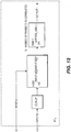
- Figure 12 shows the details of a correlator 41 1.
- the step 3 decision circuit 44 takes the outputs of the scrambled code correlators 41 1 ...41 8 , determines the correlator 41 1 ...41 8 with the maximum output, and generates an index thereof. The index is the scrambling code number.
- the scrambling code number is then forwarded to the decision support circuit 45 and the controller 18.
- the decision support circuit 45 observes the last M3 decisions made by the decision circuit 44. If a code repeats itself more than k repetitions out of M3 inputs, then the code that has been repeated is the scrambling code number that is output from the decision support circuit 45 to the controller 18.
- the output of the decision support circuit 45 is only utilized when there is no firm decision over the consecutive M3 frames. Even though the decision support circuit is only illustrated in the step 3 module 16, a decision support circuit 45 as disclosed in the step 3 module 16 can be utilized for both the step 1 and step 2 modules12, 14 disclosed herein above.
- a firm decision is indicated when the determined maximum correlation value is greater than the calculated threshold value.
- the threshold value is calculated using the noise estimator circuit 42, which is used for noise measurement, and a gain factor.
- the noise is determined by taking the magnitude of the difference between the successive common pilot symbols. This method of noise estimation eliminates any bias in the noise estimate due to orthogonal signal interference.
- the result of the noise estimator 42 is multiplied by the gain factor in the multiplier 46, which is determined to be the threshold.
- the comparator 47 outputs a high step 3 firm signal indicating a firm decision, otherwise a low signal is generated indicating a tentative decision.
- the accumulated results are forwarded to the step 3 decision circuit 44 (step 1306).
- the decision circuit 44 determines the correlator with the maximum output and generates an index thereof, which is the scrambling code number (step 1307).
- a threshold value is then calculated (step 1308) and compared to the maximum correlation value (step 1309). If the maximum correlation value is greater than the calculated threshold, the step 3 module 16 outputs a high step 3 firm signal (step 1310), which results in the decision circuit 44 outputting the scrambling code number to the controller 18 (step 1311). Otherwise, a low signal is output to the controller 18 (step 1312) and the scrambling code number is output to the decision support circuit 45 (step 1313). Since the decision support circuit 45 observes the last M3 decisions made by the decision circuit 44, a scrambling code number is output to the controller 18 when a scrambling code repeats itself k times out of M3 inputs (step 1311).
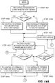
- the flow diagram of the decision logic used by the controller 18 to determine the primary scrambling code for synchronization with the transmitting base station is illustrated in Figure 14 .
- the controller 18 receives the chip offset, the step 1 firm signal and the step 1 counter signal from the step 1 module 12 (step 1401). If the step 1 firm signal is high, the controller 18 forwards the firm chip offset to the step 2 module 14 (step 1402a), otherwise a tentative chip offset is forwarded (step 1402b).
- the step 2 module 14 generates the code group number, slot offset value, step 2 firm, and step 2 counter (step 1403). If the step 2 firm signal is high, the controller forwards the firm code group to the step 3 module (step 1404a).
- the controller 18 forwards a tentative code group to the step 3 module 16 (step 1404b) and if the step 2 counter is less than M2, the step 2 module 14 continues to generate the code group number (step 1403). If the step 2 counter is equal to M2, then the step 2 module 14 is reset (step 1407), which results in the step 2 module generating a code number and slot offset (step 1403).
- the step 3 module 16 then generates a scrambling code number and step 3 firm signal (step 1405) generated in step 1403, receiving the slot offset and code group number. If the step 3 firm signal is high, then the decision logic circuit 2 determines that the scrambling code number is firm and ends the decision logic process.
- step 3 firm signal is low and the step 1 firm signal is high or the step 2 counter is less than M2, the step 2 module continues to generate a code group number (step 1403). Otherwise, the step 2 module receives a reset signal from controller 18 and resets the step 2 counter to 0 (step 1407). This procedure continues until the decision output by the step 3 module 16 is firm.
- the AFC 4 sets the frequency using the first frequency in the FAT and the offset value from the FST.
- This initial frequency is the frequency used by the controller 18 to conduct the cell search.
- the FST is a table of step frequencies, or offset frequencies, for example ⁇ 0, 2, -2, 4, -4, 6, -6...N, -N ⁇ which are used to offset the frequency in use by the controller 18.
- the FAT includes a plurality of predetermined frequencies for which the controller 18, or a level 1 controller (not shown) utilize to locate and synchronize the UE to the base station.
- the plurality of frequencies listed are defined as F 0 , F 1 , F 2 ...F N in the FAT and the offset frequencies in the FST are defined as SF 0 , SF 1 , -SF 1 , SF 2 -SF 2 ...SF N , -SF N .
- the offset frequency is SFO and the frequency > F 0 .
- the AFC 4 combines the two values F 0 +SF 0 , and forwards the resulting frequency value to the VCO or NCO 7, which maintains the UE frequency at this forwarded frequency.
- the controller 18 performs the decision logic disclosed above. If after X number of frames the output step 3 firm does not go high, the controller signals the AFC 4 to step 2 the next offset in the FST, for example, SF 1 . The AFC 4 then combines the new offset frequency with the frequency of the FAT, F 0 +SF 1 , and outputs the resulting frequency to the VCO or NCO 7 to maintain the UE at this frequency.
- the UE utilizes the detected PLMN to determine whether or not the service provider provides service in the UE's location.
- the controller 18 utilizes a window exclusion logic within the window exclusion logic circuit 6 for overcoming a rejection due to the wrong PLMN. Since detecting the HGC 21, 22 output at peak value always gives the same PLMN, the controller 18 utilizes the window exclusion logic to overcome this deadlock.
- the window exclusion logic circuit is coupled to the decision logic circuit 2, rejected chip offset vector buffer 9, a rejected chip offset counter 11, a rejected primary scrambling code vector buffer 13, and a rejected primary scrambling code counter 3.
- the window exclusion logic circuit 6 checks the primary scrambling code output from the step 3 module against the rejected primary scrambling codes stored in the rejected primary scrambling code vector buffer 13. If the primary scrambling code output from the step 3 module is found in the buffer 13, or the wrong PLMN is detected, the window exclusion logic circuit 6 rejects the code and initializes the decision logic circuit again. Each time a primary scrambling code is rejected, the chip offset that was generated by the step 1 module is stored in the rejected chip offset vector buffer 9 and used by the mask generator 5.
- the mask generator 5 of the decision circuit 25 within the step 1 module 12 uses the values stored in the rejected chip offset vector buffer 9 and rejected chip offset counter 11 from the controller 18 to determine which chips in each slot to exclude in the window. The exclusion of the detected primary scrambling codes and chip offsets are made only within a single frequency band. The buffers and counters are reset when there is an acknowledgment by the base station or new frequency band is used by the level 1 controller.
- the layer 1 controller In order to adjust the frequency band used by the controller 18 during the window exclusion logic process, the layer 1 controller signals the AFC 4 to step to the next frequency in the FAT. Since the offset frequency of the FST is set, the AFC combines the new frequency with the set offset frequency. The VCO or NCO 7 is then adjusted to maintain this combined frequency.
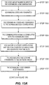
- a flow diagram of the window exclusion logic utilized by the controller is illustrated in Figure 15 .
- the controller 18 runs the cell search decision logic and finds a primary scrambling code (step 1501).
- the primary scrambling code is passed to the upper layers (step 1502) which store the frequency and the primary scrambling code index (step 1503). If the PLMN is correct for the particular service provider, the UE is synchronized to the base station, and the process is terminated (step 1504). If the PLMN is incorrect and there is a frequency remaining in the FAT of the AGC 4, the AGC 4 steps to the next frequency in the FAT and the controller 18 changes the frequency, stores the primary scrambling code in the vector buffer 13, and resets the cell search algorithm (step 1505).
- the failure condition monitors either the counter buffers 3, 11, or a timer to determine whether a failed condition occurs.
- a failed condition indicates that synchronization will not occur under the current conditions (e.g. frequency). If there is no frequency left within the FAT, the controller 18 begins to the sweep the frequencies with the stored primary scrambling code (step 1506). The controller 18 then sets the first frequency and passes the rejected primary scrambling code to the initial cell search with window exclusion method (step 1507). The controller 18 resets the initial cell search with window exclusion method and also resets the failure condition (step 1508). The rejected primary scrambling code is pushed into the rejected primary scrambling code vector buffer 13 and the rejected primary scrambling code counter is incremented (step 1509).
- the cell search decision logic is run and a primary scrambling code and chip offset are found (step 1510). If the primary scrambling code is stored in the rejected primary scrambling code vector buffer 13, then the chip offset is pushed into the rejected chip offset vector buffer 9 and the rejected chip offset counter 11 is incremented (step 1511). The cell search decision logic is again run excluding a window around the rejected chip offset (step 1512). If the primary scrambling code generated by this cell search decision logic is again stored in the rejected primary scrambling code vector buffer, then the detected chip offset is pushed onto the rejected chip offset vector buffer and the rejected chip offset counter is incremented (step 1511) and the cell search decision logic excluding a window of value rejected chip offset is run again (step 1512).
- Steps 1511 and 1512 continue until the detected primary code is not in the list at which point the primary scrambling code is forwarded to the upper layers to await an acknowledgment by the base station (step 1513). If there is a failure condition and there is no frequency left, the controller 18 indicates that no service is available (step 1517) and the process is terminated. If there was a failure and there was a frequency remaining in the bandwidth, the controller 18 sets a new frequency and passes the rejected primary scrambling code for that frequency (step 1516). The controller 18 then resets the initial cell search with window excluding method and the failure condition monitor (step 1508). The controller 18 then continues the initial cell search with window exclusion method as disclosed above.
- the controller 18 indicates that the UE is synchronized to the base station upon receipt of the acknowledgment (step 1518), and the process is terminated. If the PLMN is incorrect, the rejected primary scrambling code is pushed into the rejected primary scrambling code vector buffer 13 and the rejected primary scrambling code counter 3 is incremented (step 1515). The cell search decision logic is run again excluding a window around the previously rejected chip offset value (step 1512). This procedure continues until the controller indicates that no service is available or an acknowledgment from a base station is received.
Landscapes
- Engineering & Computer Science (AREA)
- Computer Networks & Wireless Communication (AREA)
- Signal Processing (AREA)
- Databases & Information Systems (AREA)
- Computer Security & Cryptography (AREA)
- Mobile Radio Communication Systems (AREA)
- Synchronisation In Digital Transmission Systems (AREA)
- Supplying Of Containers To The Packaging Station (AREA)
- Data Exchanges In Wide-Area Networks (AREA)
Claims (5)
- Benutzergerät (User Equipment, UE)-Einheit, die fähig ist, eine Anfangszellensuche durchzuführen und eine Kommunikationsverbindung mit einer Basisstation in einem Kommunikationsnetzwerk herzustellen, wobei das UE Folgendes umfasst:ein erstes Modul (12), das konfiguriert ist, um ein Kommunikationssignal zu verarbeiten, und einem Spitzenabtastwert des Kommunikationssignals einen Indexwert zuzuordnen, wobei der Indexwert verwendet wird, um einen Chipversatz eines primären Verwürfelungscodes zu berechnen; undein zweites Modul (14), das konfiguriert ist, um den berechneten Chipversatz zu verwenden, um eine Verwürfelungscode-Gruppennummer, einen Slotversatz und einen sekundären Synchronisationscode des Kommunikationssignals zu erkennen;ein drittes Modul (16), das konfiguriert ist, um den durch das erste Modul (12) berechneten Chipversatz sowie die Verwürfelungscode-Gruppennummer und den Slotversatz, die von dem zweiten Modul (14) erkannt wurden, zu empfangen, wobei das dritte Modul (16) konfiguriert ist, um einen primären Verwürfelungscode aus dem Kommunikationssignal basierend auf dem Chipversatz, der Verwürfelungscode-Gruppennummer und dem Slotversatz abzurufen;eine Steuerung (18), die mit dem ersten Modul (12), dem zweiten Modul (14) und dem dritten Modul (16) gekoppelt ist,wobei das UE dadurch gekennzeichnet ist, dass:die Steuerung (18) konfiguriert ist, um eine Anpassung einer Suchfrequenz in dem UE zu steuern, damit das dritte Modul (16) den primären Verwürfelungscode in dem Kommunikationssignal abrufen kann; wobei die Steuerung (18) Folgendes aufweist:einen ersten Puffer (13), der konfiguriert ist, um abgelehnte primäre Verwürfelungscodes zu speichern;einen zweiten Puffer (9), der konfiguriert ist, um abgelehnte Chipversatz-Vektoren zu speichern; undeine Entscheidungslogikschaltung (2), die konfiguriert ist, um zu bestimmen, ob der erkannte Verwürfelungscode korrekt ist;wobei das erste Modul (12) ferner einen Maskengenerator (5) aufweist, wobei der Maskengenerator (5) des ersten Moduls (12) konfiguriert ist, um zu bestimmen, welche Chips in jedem Slot durch die Entscheidungslogikschaltung (2) von der Erkennung ausgeschlossen werden sollen, wobei die ausgeschlossenen Chips basierend auf Chipversätzen bestimmt werden, die in dem zweiten Puffer (9) gespeichert sind.
- UE nach Anspruch 1, ferner umfassend einen Frequenzsynthesizer (20), der auf die Steuerung anspricht und konfiguriert ist, um die Suchfrequenz anzupassen und zu erhalten, wobei der Synthesizer einen Oszillator (7) und eine adaptive Frequenzschaltung (Adaptive Frequency Circuit, AFC) (4) aufweist, die konfiguriert ist, um die Suchfrequenz durch Kombinieren einer Vielzahl von Versatzfrequenzen mit einer von mehreren Basisfrequenzen zu erzeugen, wobei die AFC Folgendes umfasst:eine Frequenzschritttabelle, die die Vielzahl von Versatzfrequenzen aufweist; undeine Frequenzzuteilungstabelle, die die Vielzahl von Basisfrequenzen aufweist.
- UE nach Anspruch 2, wobei der Oszillator (7) ein spannungsgesteuerter Oszillator oder ein numerisch gesteuerter Oszillator ist, wobei der Oszillator auf die AFC anspricht, um das UE auf der Suchfrequenz zu erhalten.
- UE nach Anspruch 1, wobei die Steuerung (18) konfiguriert ist, um die Suchfrequenz durch Extrahieren einer einer Vielzahl von Versatzfrequenzen und einer einer Vielzahl von Suchfrequenzen und Kombinieren der Versatz- und Suchfrequenzen anzupassen.
- UE nach Anspruch 1, wobei die Steuerung (18) ferner Folgendes umfasst:eine Fensterausschlussschaltung, gekoppelt mit dem ersten Puffer, dem zweiten Puffer und der Entscheidungslogikschaltung, die konfiguriert ist, um öffentliche landgestützte Mobilfunknetze (Public Mobile Land Networks, PMLNs) zu erkennen und einen von einem falschen PMLN verursachten Ausschluss zu überwinden, wobei die Fensterausschlussschaltung Chips ausschließen soll, die durch die Maske (5) des ersten Moduls (12) bestimmt werden.
Applications Claiming Priority (4)
| Application Number | Priority Date | Filing Date | Title |
|---|---|---|---|
| US27164201P | 2001-02-27 | 2001-02-27 | |
| US09/918,611 US6826244B2 (en) | 2001-02-27 | 2001-07-31 | Initial cell search algorithm for 3G FDD wireless communication systems |
| EP02702141A EP1380131B1 (de) | 2001-02-27 | 2002-02-04 | Anfangszellensuchalgorithmus |
| EP06111667A EP1686698B1 (de) | 2001-02-27 | 2002-02-04 | Anfangszellensuchalgorithmus |
Related Parent Applications (2)
| Application Number | Title | Priority Date | Filing Date |
|---|---|---|---|
| EP06111667A Division EP1686698B1 (de) | 2001-02-27 | 2002-02-04 | Anfangszellensuchalgorithmus |
| EP02702141A Division EP1380131B1 (de) | 2001-02-27 | 2002-02-04 | Anfangszellensuchalgorithmus |
Publications (3)
| Publication Number | Publication Date |
|---|---|
| EP1833175A1 EP1833175A1 (de) | 2007-09-12 |
| EP1833175A8 EP1833175A8 (de) | 2008-04-16 |
| EP1833175B1 true EP1833175B1 (de) | 2017-11-01 |
Family
ID=26955047
Family Applications (5)
| Application Number | Title | Priority Date | Filing Date |
|---|---|---|---|
| EP09173326A Withdrawn EP2148448A1 (de) | 2001-02-27 | 2002-02-04 | Anfangszellensuchalgorithmus |
| EP06111667A Expired - Lifetime EP1686698B1 (de) | 2001-02-27 | 2002-02-04 | Anfangszellensuchalgorithmus |
| EP02702141A Expired - Lifetime EP1380131B1 (de) | 2001-02-27 | 2002-02-04 | Anfangszellensuchalgorithmus |
| EP05108806A Expired - Lifetime EP1608080B8 (de) | 2001-02-27 | 2002-02-04 | Anfangszellensuchalgorithmus |
| EP07111143.9A Expired - Lifetime EP1833175B1 (de) | 2001-02-27 | 2002-02-04 | Anfangszellensuchalgorithmus |
Family Applications Before (4)
| Application Number | Title | Priority Date | Filing Date |
|---|---|---|---|
| EP09173326A Withdrawn EP2148448A1 (de) | 2001-02-27 | 2002-02-04 | Anfangszellensuchalgorithmus |
| EP06111667A Expired - Lifetime EP1686698B1 (de) | 2001-02-27 | 2002-02-04 | Anfangszellensuchalgorithmus |
| EP02702141A Expired - Lifetime EP1380131B1 (de) | 2001-02-27 | 2002-02-04 | Anfangszellensuchalgorithmus |
| EP05108806A Expired - Lifetime EP1608080B8 (de) | 2001-02-27 | 2002-02-04 | Anfangszellensuchalgorithmus |
Country Status (19)
| Country | Link |
|---|---|
| US (7) | US6826244B2 (de) |
| EP (5) | EP2148448A1 (de) |
| JP (2) | JP4382352B2 (de) |
| KR (2) | KR100722210B1 (de) |
| CN (2) | CN101174853B (de) |
| AR (1) | AR032861A1 (de) |
| AT (3) | ATE390766T1 (de) |
| BR (1) | BRPI0207841B1 (de) |
| CA (2) | CA2439378C (de) |
| DE (4) | DE60216162T2 (de) |
| DK (3) | DK1686698T3 (de) |
| ES (4) | ES2344402T3 (de) |
| IL (3) | IL157450A0 (de) |
| MX (1) | MXPA03007640A (de) |
| MY (1) | MY130625A (de) |
| NO (2) | NO336023B1 (de) |
| SG (2) | SG190452A1 (de) |
| TW (5) | TWI342681B (de) |
| WO (1) | WO2002069551A1 (de) |
Families Citing this family (28)
| Publication number | Priority date | Publication date | Assignee | Title |
|---|---|---|---|---|
| CA2406438C (en) | 2000-04-07 | 2006-10-17 | Interdigital Technology Corporation | Base station synchronization for wireless communication systems |
| TW532041B (en) | 2000-08-04 | 2003-05-11 | Interdigital Tech Corp | Cell search |
| US6826244B2 (en) | 2001-02-27 | 2004-11-30 | Interdigital Technology Corporation | Initial cell search algorithm for 3G FDD wireless communication systems |
| GB2378328B (en) * | 2001-08-01 | 2005-07-13 | Ipwireless Inc | AGC scheme and receiver for use in a wireless communication system |
| US7356098B2 (en) | 2001-11-14 | 2008-04-08 | Ipwireless, Inc. | Method, communication system and communication unit for synchronisation for multi-rate communication |
| TWI224740B (en) * | 2002-07-31 | 2004-12-01 | Interdigital Tech Corp | Start-up automatic frequency control (AFC) method and apparatus |
| US7415084B2 (en) * | 2002-09-12 | 2008-08-19 | Interdigital Technology Corporation | Mitigation of interference in cell search by wireless transmit and receive units |
| US20040058650A1 (en) * | 2002-09-19 | 2004-03-25 | Torgny Palenius | Receivers and methods for searching for cells using recorded data |
| AU2003259590A1 (en) * | 2003-01-23 | 2004-08-12 | Nec Australia Pty Ltd | Cell search method and apparatus in a WCDMA system |
| EP1978662A1 (de) * | 2003-02-05 | 2008-10-08 | Interdigital Technology Corporation | Anfangszellensuche in drahtlosen Kommunikationssystemen |
| US7555067B2 (en) * | 2003-03-13 | 2009-06-30 | Texas Instruments Incorporated | Method and apparatus for decoder input scaling based on interference estimation in CDMA |
| DE10311323A1 (de) * | 2003-03-14 | 2004-09-30 | Infineon Technologies Ag | Vorrichtung zur Synchronisation eines Mobilfunkempfängers auf eine Rahmenstruktur eines empfangenen Funksignals |
| US7261830B2 (en) * | 2003-10-16 | 2007-08-28 | Molecular Imprints, Inc. | Applying imprinting material to substrates employing electromagnetic fields |
| US8364185B2 (en) * | 2005-04-18 | 2013-01-29 | Samsung Electronics Co., Ltd. | Method and system for synchronizing a clock for an adjacent network to a clock for an overlay network |
| JP2006319765A (ja) * | 2005-05-13 | 2006-11-24 | Mitsubishi Electric Corp | Cdma用受信装置およびセルサーチ方法 |
| US9094146B2 (en) | 2007-01-08 | 2015-07-28 | Telefonaktiebolaget Lm Ericsson (Publ) | Secondary synchronization sequences for cell group detection in a cellular communications system |
| US8050225B2 (en) * | 2007-05-21 | 2011-11-01 | Qualcomm Incorporated | Assignment of primary and secondary synchronization code sequences to cells in a wireless communication system |
| US9025586B2 (en) * | 2007-09-21 | 2015-05-05 | Texas Instruments Incorporated | Secondary synchronization signal mapping |
| US8503547B2 (en) * | 2007-10-11 | 2013-08-06 | Qualcomm Incorporated | Scrambling codes for secondary synchronization codes in wireless communication systems |
| EP2117128B1 (de) | 2008-05-09 | 2012-11-21 | Research In Motion Limited | Abtastverfahren und Vorrichtung zur Systemerfassung |
| US8098630B2 (en) | 2008-05-09 | 2012-01-17 | Research In Motion Limited | Scanning methods and apparatus for system acquisition |
| US8849452B2 (en) * | 2009-08-03 | 2014-09-30 | Honda Motor Co., Ltd. | Robot and control system |
| EP2456106B1 (de) * | 2010-11-22 | 2013-11-06 | Sequans Communications | Zellensuchverfahren für einen Abwärtskanal eines OFDMA-Übertragungssystems |
| US8748798B2 (en) * | 2012-09-05 | 2014-06-10 | Omnivision Technologies, Inc. | Comparator circuit for reduced output variation |
| US10474652B2 (en) * | 2013-03-14 | 2019-11-12 | Inpixon | Optimizing wide data-type storage and analysis of data in a column store database |
| US10305671B2 (en) * | 2015-05-21 | 2019-05-28 | Cirrus Logic, Inc. | Synchronous differential signaling protocol |
| US10044403B1 (en) * | 2017-05-04 | 2018-08-07 | Samsung Electronics Co., Ltd | Apparatus and method for multi-beam initial synchronization for 5G-NR system |
| US10624024B2 (en) * | 2017-10-24 | 2020-04-14 | Qualcomm Incorporated | Correlation-enhanced frequency scanning |
Citations (1)
| Publication number | Priority date | Publication date | Assignee | Title |
|---|---|---|---|---|
| WO2001001596A1 (en) * | 1999-06-30 | 2001-01-04 | Qualcomm Incorporated | Method and apparatus for fast wcdma acquisition |
Family Cites Families (84)
| Publication number | Priority date | Publication date | Assignee | Title |
|---|---|---|---|---|
| US421941A (en) * | 1890-02-25 | leeds | ||
| US9930A (en) * | 1853-08-09 | Improvement in grain harvesters and binders | ||
| US110160A (en) * | 1870-12-13 | Improvement in anti-friction boxes for axles | ||
| US4661A (en) * | 1846-07-24 | Improvement in magnetic fire-alarms | ||
| US288239A (en) * | 1883-11-13 | George a | ||
| US387168A (en) * | 1888-07-31 | Rotating trolling device for shipsj logs | ||
| US44117A (en) * | 1864-09-06 | Improved composition for concrete pavements | ||
| US378440A (en) * | 1888-02-28 | Electric railway-station indicator | ||
| US101596A (en) * | 1870-04-05 | Improvement in revolving center-rest for wood-lathes | ||
| US14907A (en) * | 1856-05-20 | Printing-machine | ||
| US319998A (en) * | 1885-06-16 | Chaeles g | ||
| US391101A (en) * | 1887-09-28 | 1888-10-16 | Howaed w | |
| US828910A (en) * | 1903-05-25 | 1906-08-21 | Day J H Co | Mixing-machine. |
| US854122A (en) * | 1905-08-10 | 1907-05-21 | Simon B Storer | System of electrical distribution. |
| US825737A (en) * | 1905-11-03 | 1906-07-10 | Thomas Lauther | Curtain-fixture. |
| US852430A (en) * | 1906-12-15 | 1907-05-07 | William L Goodman | Ruling apparatus. |
| US1414482A (en) * | 1921-05-07 | 1922-05-02 | Nelson John | Manufacture of carbon for pigmental and other purposes |
| FI920976A0 (fi) * | 1992-03-05 | 1992-03-05 | Tecnomen Oy | Radiosynkroniseringsfoerfarande foer stoedstationer i ett simulcastingnaet. |
| US5313457A (en) * | 1992-04-14 | 1994-05-17 | Trimble Navigation Limited | Code position modulation system and method for multiple user satellite communications |
| SE470037C (sv) | 1992-10-27 | 1995-04-10 | Ericsson Telefon Ab L M | Anordning vid mobila telekommunikationssystem för att möjliggöra synkronisering av basstationernas sändare |
| US5448570A (en) | 1993-03-17 | 1995-09-05 | Kyocera Corporation | System for mutual synchronization and monitoring between base stations |
| WO1994028643A1 (en) | 1993-05-27 | 1994-12-08 | Nokia Telecommunications Oy | Base station for a tdma cellular radio network |
| EP0659326B1 (de) * | 1993-06-14 | 2002-09-04 | Telefonaktiebolaget Lm Ericsson | Übertragungszeitjustierung in der abwärtsverbindung eines systems mit kodemultiplex-vielfachzugriff |
| JPH0825737A (ja) * | 1994-07-13 | 1996-01-30 | Canon Inc | 画像形成装置 |
| US5881100A (en) * | 1994-09-09 | 1999-03-09 | Omnipoint Corporation | Method and apparatus for coherent correlation of a spread spectrum signal |
| US5784368A (en) | 1994-09-23 | 1998-07-21 | Motorola, Inc. | Method and apparatus for providing a synchronous communication environment |
| KR100201806B1 (ko) * | 1994-10-19 | 1999-06-15 | 윤종용 | 무선호출수신기의전원 절약장치 및 방법 |
| JP3116264B2 (ja) | 1994-12-07 | 2000-12-11 | 松下電器産業株式会社 | スペクトル拡散通信受信機 |
| US6177964B1 (en) * | 1997-08-01 | 2001-01-23 | Microtune, Inc. | Broadband integrated television tuner |
| US6049535A (en) * | 1996-06-27 | 2000-04-11 | Interdigital Technology Corporation | Code division multiple access (CDMA) communication system |
| JP3208305B2 (ja) * | 1995-11-14 | 2001-09-10 | シャープ株式会社 | 通信装置および通信方法 |
| US5793772A (en) * | 1995-11-29 | 1998-08-11 | Motorola, Inc. | Method and apparatus for synchronizing timing of components of a telecommunication system |
| CN1080047C (zh) | 1996-03-05 | 2002-02-27 | Ntt移动通信网株式会社 | 移动通信系统中的信号传输方法,发射机,接收机和扩展码同步法 |
| US6014376A (en) | 1996-09-18 | 2000-01-11 | Motorola, Inc. | Method for over-the-air synchronization adjustment in a communication system |
| JP3376224B2 (ja) * | 1996-10-23 | 2003-02-10 | 株式会社エヌ・ティ・ティ・ドコモ | Ds−cdma基地局間非同期セルラ方式における初期同期方法および受信機 |
| JP2845228B2 (ja) | 1996-12-10 | 1999-01-13 | 日本電気株式会社 | 隣接セル同期検出方式 |
| JPH10190562A (ja) | 1996-12-26 | 1998-07-21 | Toshiba Corp | 移動通信システムの基地局間フレーム同期方式およびこの方式を適用した基地局装置 |
| JP3373746B2 (ja) * | 1997-01-07 | 2003-02-04 | 株式会社鷹山 | Ds−cdma基地局間非同期セルラ方式における初期同期方法および受信機 |
| SE9700896L (sv) * | 1997-03-13 | 1998-02-09 | Kockum Sonics Ab | Ljudgenerator |
| JPH10304437A (ja) | 1997-04-30 | 1998-11-13 | Fujitsu Ltd | 無線区間同期監視方式及び該方式による無線基地局装置 |
| US6597914B1 (en) * | 1997-05-09 | 2003-07-22 | Nokia Corporation | Method for determining timing differences between radio transmitters and a radio network incorporating the same |
| US5991330A (en) | 1997-06-27 | 1999-11-23 | Telefonaktiebolaget L M Ericsson (Pub1) | Mobile Station synchronization within a spread spectrum communication systems |
| US5930366A (en) | 1997-08-29 | 1999-07-27 | Telefonaktiebolaget L M Ericsson | Synchronization to a base station and code acquisition within a spread spectrum communication system |
| US5872774A (en) | 1997-09-19 | 1999-02-16 | Qualcomm Incorporated | Mobile station assisted timing synchronization in a CDMA communication system |
| CN100590988C (zh) | 1997-10-10 | 2010-02-17 | 高通股份有限公司 | 扩展谱通信系统中对信息信号进行扩展的装置 |
| JP3385200B2 (ja) | 1997-11-07 | 2003-03-10 | 株式会社エヌ・ティ・ティ・ドコモ | 移動通信システムにおける信号の伝送方法および拡散符号同期法 |
| FI974310A7 (fi) | 1997-11-24 | 1999-05-25 | Nokia Networks Oy | Menetelmä tukiasemien synkronisoimiseksi ja solukkoradiojärjestelmä |
| RU2241312C2 (ru) | 1998-02-12 | 2004-11-27 | Телефонактиеболагет Лм Эрикссон (Пабл) | Система и способ обеспечения синхронизации базовых станций в асинхронной системе мобильной связи множественного доступа с кодовым разделением каналов |
| TW428388B (en) | 1998-02-20 | 2001-04-01 | Koninkl Philips Electronics Nv | A power consumption reduction method in a digital mobile radio system and a mobile radio station |
| US6208871B1 (en) * | 1998-02-27 | 2001-03-27 | Motorola, Inc. | Method and apparatus for providing a time adjustment to a wireless communication system |
| JP3090117B2 (ja) | 1998-03-26 | 2000-09-18 | 株式会社デンソー | スペクトラム拡散信号復調装置 |
| EP0954122A1 (de) | 1998-04-28 | 1999-11-03 | Siemens Aktiengesellschaft | Verfahren zum Betreiben eines Funk-Kommunikationssystems und derartiges Funk-Kommunikationssystem |
| US6230018B1 (en) * | 1998-05-14 | 2001-05-08 | Nortel Networks Limited | Devices and processing in a mobile radio communication network having calibration terminals |
| US6504830B1 (en) | 1998-06-15 | 2003-01-07 | Telefonaktiebolaget Lm Ericsson Publ | Method, apparatus, and system for fast base synchronization and sector identification |
| DE19831569A1 (de) | 1998-07-14 | 2000-01-20 | Siemens Ag | Verfahren zur Informationsübertragung und Funkstation |
| EP0977351B1 (de) * | 1998-07-30 | 2004-02-18 | Motorola Semiconducteurs S.A. | Verfahren und Gerät zur Funkübertragung |
| US6131030A (en) | 1998-08-19 | 2000-10-10 | Telefonaktiebolaget Lm Ericsson | System network and method for the transference of cell handover information |
| GB9819482D0 (en) | 1998-09-07 | 1998-10-28 | Nokia Telecommunications Oy | Communication system |
| US6539004B1 (en) * | 1998-09-17 | 2003-03-25 | Lucent Technologies Inc. | Time synchronization of packetized radio signals to base stations |
| US6223037B1 (en) | 1998-10-09 | 2001-04-24 | Nokia Mobile Phones Ltd. | Cell selection during loss of service in a telecommunications system |
| US6205334B1 (en) * | 1998-11-24 | 2001-03-20 | Ericsson Inc. | Accelerated scanning of cellular channels by cellular radiotelephones |
| JP3428965B2 (ja) * | 1998-12-01 | 2003-07-22 | サムスン エレクトロニクス カンパニー リミテッド | 直交周波数分割多重/符号分割多重接続システムの周波数同期装置 |
| US6590881B1 (en) | 1998-12-04 | 2003-07-08 | Qualcomm, Incorporated | Method and apparatus for providing wireless communication system synchronization |
| US6522706B1 (en) * | 1998-12-10 | 2003-02-18 | National Semiconductor Corporation | Delay spread estimation for multipath fading channels |
| US6625200B1 (en) * | 1999-01-25 | 2003-09-23 | Ericsson Inc. | Multi-stage CDMA synchronization with parallel execution |
| AU3383400A (en) | 1999-02-26 | 2000-09-14 | Qualcomm Incorporated | Method and system for handoff between an asynchronous cdma base station and a synchronous cdma base station |
| FI107487B (fi) * | 1999-03-08 | 2001-08-15 | Nokia Mobile Phones Ltd | Datalähetyksen salausmenetelmä radiojärjestelmässä |
| US6480558B1 (en) | 1999-03-17 | 2002-11-12 | Ericsson Inc. | Synchronization and cell search methods and apparatus for wireless communications |
| KR20000073917A (ko) * | 1999-05-15 | 2000-12-05 | 윤종용 | 비동기식 부호분할다중접속 통신시스템의 동기워드 생성 및 송수신장치 및 방법 |
| US6493380B1 (en) * | 1999-05-28 | 2002-12-10 | Nortel Networks Limited | System and method for estimating signal time of arrival |
| US6483824B1 (en) * | 1999-07-29 | 2002-11-19 | Qualcomm, Inc. | Method and apparatus for acquiring service in a “border area” |
| US6834046B1 (en) * | 1999-10-05 | 2004-12-21 | Texas Instruments Incorporated | Acquisition of an unevenly spaced synchronization channel in a wireless communication system |
| US6996162B1 (en) * | 1999-10-05 | 2006-02-07 | Texas Instruments Incorporated | Correlation using only selected chip position samples in a wireless communication system |
| JP3439399B2 (ja) | 1999-10-14 | 2003-08-25 | エヌイーシーマイクロシステム株式会社 | Cdmaベースバンド受信装置 |
| TW486914B (en) | 1999-12-02 | 2002-05-11 | Ericsson Telefon Ab L M | Synchronization of diversity handover destination base station |
| KR100319927B1 (ko) * | 2000-01-11 | 2002-01-09 | 윤종용 | 비동기식 광대역 직접 시퀀스 코드분할다중접속 수신기의셀 탐색 장치 및 각 셀에 고유한 코드 획득 방법 |
| US7047011B1 (en) | 2000-02-10 | 2006-05-16 | Telefonaktiebolaget Lm Ericsson (Publ) | Synchronization in diversity handover |
| CA2406438C (en) | 2000-04-07 | 2006-10-17 | Interdigital Technology Corporation | Base station synchronization for wireless communication systems |
| EP1387594B1 (de) | 2000-05-10 | 2006-07-26 | Mitsubishi Electric Information Technology Centre Europe B.V. | Verfahren zur Zuweisung von Sekundärsynchronisationscodes an eine Basisstation eines Mobilkommunikationssystems |
| FR2811367B1 (fr) * | 2000-07-04 | 2003-02-14 | Meritor Light Vehicle Sys Ltd | Leve-vitre ayant un curseur a deplacement silencieux |
| WO2002058334A2 (en) | 2001-01-18 | 2002-07-25 | Strix Systems, Inc. | System, method and computer-readable medium for wirelessly exchanging communication with a mobile unit |
| US6826244B2 (en) | 2001-02-27 | 2004-11-30 | Interdigital Technology Corporation | Initial cell search algorithm for 3G FDD wireless communication systems |
| US6476572B2 (en) * | 2001-04-03 | 2002-11-05 | Overhead Door Corporation | Power supply system and method for dock equipment |
| US20030203745A1 (en) | 2002-04-30 | 2003-10-30 | Chiang Tung Ching | Assisted base stations synchronization |
-
2001
- 2001-07-31 US US09/918,611 patent/US6826244B2/en not_active Expired - Lifetime
-
2002
- 2002-02-04 DE DE60216162T patent/DE60216162T2/de not_active Expired - Lifetime
- 2002-02-04 ES ES02702141T patent/ES2344402T3/es not_active Expired - Lifetime
- 2002-02-04 CA CA002439378A patent/CA2439378C/en not_active Expired - Lifetime
- 2002-02-04 KR KR1020037013853A patent/KR100722210B1/ko not_active Expired - Lifetime
- 2002-02-04 DE DE60236076T patent/DE60236076D1/de not_active Expired - Lifetime
- 2002-02-04 JP JP2002568557A patent/JP4382352B2/ja not_active Expired - Lifetime
- 2002-02-04 MX MXPA03007640A patent/MXPA03007640A/es active IP Right Grant
- 2002-02-04 EP EP09173326A patent/EP2148448A1/de not_active Withdrawn
- 2002-02-04 DE DE0001380131T patent/DE02702141T1/de active Pending
- 2002-02-04 CA CA2599806A patent/CA2599806C/en not_active Expired - Lifetime
- 2002-02-04 KR KR1020037011261A patent/KR100649064B1/ko not_active Expired - Fee Related
- 2002-02-04 IL IL15745002A patent/IL157450A0/xx unknown
- 2002-02-04 ES ES07111143.9T patent/ES2657475T3/es not_active Expired - Lifetime
- 2002-02-04 CN CN2007101669747A patent/CN101174853B/zh not_active Expired - Lifetime
- 2002-02-04 DK DK06111667T patent/DK1686698T3/da active
- 2002-02-04 BR BRPI0207841A patent/BRPI0207841B1/pt not_active IP Right Cessation
- 2002-02-04 DK DK02702141.9T patent/DK1380131T3/da active
- 2002-02-04 EP EP06111667A patent/EP1686698B1/de not_active Expired - Lifetime
- 2002-02-04 ES ES05108806T patent/ES2273312T3/es not_active Expired - Lifetime
- 2002-02-04 DK DK05108806T patent/DK1608080T3/da active
- 2002-02-04 CN CNB028055926A patent/CN100346591C/zh not_active Expired - Lifetime
- 2002-02-04 EP EP02702141A patent/EP1380131B1/de not_active Expired - Lifetime
- 2002-02-04 AT AT06111667T patent/ATE390766T1/de not_active IP Right Cessation
- 2002-02-04 SG SG2010012920A patent/SG190452A1/en unknown
- 2002-02-04 WO PCT/US2002/003217 patent/WO2002069551A1/en not_active Ceased
- 2002-02-04 EP EP05108806A patent/EP1608080B8/de not_active Expired - Lifetime
- 2002-02-04 SG SG200505528-0A patent/SG132508A1/en unknown
- 2002-02-04 ES ES06111667T patent/ES2304181T3/es not_active Expired - Lifetime
- 2002-02-04 AT AT05108806T patent/ATE345601T1/de not_active IP Right Cessation
- 2002-02-04 DE DE60225861T patent/DE60225861T2/de not_active Expired - Lifetime
- 2002-02-04 EP EP07111143.9A patent/EP1833175B1/de not_active Expired - Lifetime
- 2002-02-04 AT AT02702141T patent/ATE465555T1/de not_active IP Right Cessation
- 2002-02-07 TW TW095139071A patent/TWI342681B/zh not_active IP Right Cessation
- 2002-02-07 TW TW091102284A patent/TWI268110B/zh not_active IP Right Cessation
- 2002-02-07 TW TW094121510A patent/TWI321913B/zh not_active IP Right Cessation
- 2002-02-07 TW TW092127536A patent/TWI250425B/zh not_active IP Right Cessation
- 2002-02-07 TW TW099106045A patent/TWI428042B/zh not_active IP Right Cessation
- 2002-02-26 AR ARP020100658A patent/AR032861A1/es not_active Application Discontinuation
- 2002-02-27 US US10/083,796 patent/US7046754B2/en not_active Expired - Fee Related
- 2002-02-27 MY MYPI20020699A patent/MY130625A/en unknown
- 2002-04-11 US US10/120,735 patent/US6804315B2/en not_active Expired - Lifetime
-
2003
- 2003-08-18 IL IL157450A patent/IL157450A/en unknown
- 2003-08-25 NO NO20033770A patent/NO336023B1/no not_active IP Right Cessation
-
2005
- 2005-08-17 US US11/205,846 patent/US7433437B2/en not_active Expired - Lifetime
-
2007
- 2007-07-10 JP JP2007181460A patent/JP4718520B2/ja not_active Expired - Lifetime
-
2008
- 2008-10-06 IL IL194548A patent/IL194548A/en active IP Right Grant
- 2008-10-06 US US12/245,800 patent/US7746920B2/en not_active Expired - Fee Related
-
2010
- 2010-04-07 US US12/755,583 patent/US8503512B2/en not_active Expired - Fee Related
-
2013
- 2013-07-25 US US13/951,303 patent/US9247509B2/en not_active Expired - Fee Related
-
2015
- 2015-01-06 NO NO20150027A patent/NO342203B1/no not_active IP Right Cessation
Patent Citations (1)
| Publication number | Priority date | Publication date | Assignee | Title |
|---|---|---|---|---|
| WO2001001596A1 (en) * | 1999-06-30 | 2001-01-04 | Qualcomm Incorporated | Method and apparatus for fast wcdma acquisition |
Also Published As
Similar Documents
| Publication | Publication Date | Title |
|---|---|---|
| EP1686698B1 (de) | Anfangszellensuchalgorithmus | |
| HK1116936B (en) | Initial cell search algorithm | |
| HK1116936A (en) | Initial cell search algorithm | |
| HK1117664B (en) | Initial cell search algorithm | |
| KR100311528B1 (ko) | 기지국 탐색 방법 및 그를 위한 수신 장치 |
Legal Events
| Date | Code | Title | Description |
|---|---|---|---|
| PUAI | Public reference made under article 153(3) epc to a published international application that has entered the european phase |
Free format text: ORIGINAL CODE: 0009012 |
|
| 17P | Request for examination filed |
Effective date: 20070627 |
|
| AC | Divisional application: reference to earlier application |
Ref document number: 1686698 Country of ref document: EP Kind code of ref document: P Ref document number: 1380131 Country of ref document: EP Kind code of ref document: P |
|
| AK | Designated contracting states |
Kind code of ref document: A1 Designated state(s): AT BE CH CY DE DK ES FI FR GB GR IE IT LI LU MC NL PT SE TR |
|
| 17Q | First examination report despatched |
Effective date: 20080409 |
|
| AKX | Designation fees paid |
Designated state(s): AT BE CH CY DE DK ES FI FR GB GR IE IT LI LU MC NL PT SE TR |
|
| REG | Reference to a national code |
Ref country code: HK Ref legal event code: DE Ref document number: 1116936 Country of ref document: HK |
|
| RAP1 | Party data changed (applicant data changed or rights of an application transferred) |
Owner name: INTEL CORPORATION |
|
| REG | Reference to a national code |
Ref country code: DE Ref legal event code: R079 Ref document number: 60249152 Country of ref document: DE Free format text: PREVIOUS MAIN CLASS: H04B0001707000 Ipc: H04B0001708300 |
|
| GRAP | Despatch of communication of intention to grant a patent |
Free format text: ORIGINAL CODE: EPIDOSNIGR1 |
|
| RIC1 | Information provided on ipc code assigned before grant |
Ipc: H04J 3/06 20060101ALI20170308BHEP Ipc: H04B 1/7083 20110101AFI20170308BHEP Ipc: H04J 11/00 20060101ALI20170308BHEP Ipc: H04W 56/00 20090101ALI20170308BHEP Ipc: H04W 48/16 20090101ALI20170308BHEP |
|
| INTG | Intention to grant announced |
Effective date: 20170406 |
|
| GRAS | Grant fee paid |
Free format text: ORIGINAL CODE: EPIDOSNIGR3 |
|
| GRAA | (expected) grant |
Free format text: ORIGINAL CODE: 0009210 |
|
| AC | Divisional application: reference to earlier application |
Ref document number: 1380131 Country of ref document: EP Kind code of ref document: P Ref document number: 1686698 Country of ref document: EP Kind code of ref document: P |
|
| AK | Designated contracting states |
Kind code of ref document: B1 Designated state(s): AT BE CH CY DE DK ES FI FR GB GR IE IT LI LU MC NL PT SE TR |
|
| REG | Reference to a national code |
Ref country code: GB Ref legal event code: FG4D |
|
| REG | Reference to a national code |
Ref country code: CH Ref legal event code: EP Ref country code: AT Ref legal event code: REF Ref document number: 942994 Country of ref document: AT Kind code of ref document: T Effective date: 20171115 |
|
| REG | Reference to a national code |
Ref country code: IE Ref legal event code: FG4D |
|
| REG | Reference to a national code |
Ref country code: DE Ref legal event code: R096 Ref document number: 60249152 Country of ref document: DE |
|
| REG | Reference to a national code |
Ref country code: FR Ref legal event code: PLFP Year of fee payment: 17 |
|
| REG | Reference to a national code |
Ref country code: NL Ref legal event code: FP |
|
| REG | Reference to a national code |
Ref country code: ES Ref legal event code: FG2A Ref document number: 2657475 Country of ref document: ES Kind code of ref document: T3 Effective date: 20180305 |
|
| PG25 | Lapsed in a contracting state [announced via postgrant information from national office to epo] |
Ref country code: SE Free format text: LAPSE BECAUSE OF FAILURE TO SUBMIT A TRANSLATION OF THE DESCRIPTION OR TO PAY THE FEE WITHIN THE PRESCRIBED TIME-LIMIT Effective date: 20171101 Ref country code: FI Free format text: LAPSE BECAUSE OF FAILURE TO SUBMIT A TRANSLATION OF THE DESCRIPTION OR TO PAY THE FEE WITHIN THE PRESCRIBED TIME-LIMIT Effective date: 20171101 |
|
| PGFP | Annual fee paid to national office [announced via postgrant information from national office to epo] |
Ref country code: ES Payment date: 20180301 Year of fee payment: 17 |
|
| REG | Reference to a national code |
Ref country code: HK Ref legal event code: GR Ref document number: 1116936 Country of ref document: HK |
|
| PGFP | Annual fee paid to national office [announced via postgrant information from national office to epo] |
Ref country code: GR Payment date: 20180201 Year of fee payment: 17 |
|
| REG | Reference to a national code |
Ref country code: GR Ref legal event code: EP Ref document number: 20180400314 Country of ref document: GR Effective date: 20180518 |
|
| PG25 | Lapsed in a contracting state [announced via postgrant information from national office to epo] |
Ref country code: CY Free format text: LAPSE BECAUSE OF FAILURE TO SUBMIT A TRANSLATION OF THE DESCRIPTION OR TO PAY THE FEE WITHIN THE PRESCRIBED TIME-LIMIT Effective date: 20171101 Ref country code: DK Free format text: LAPSE BECAUSE OF FAILURE TO SUBMIT A TRANSLATION OF THE DESCRIPTION OR TO PAY THE FEE WITHIN THE PRESCRIBED TIME-LIMIT Effective date: 20171101 |
|
| REG | Reference to a national code |
Ref country code: DE Ref legal event code: R097 Ref document number: 60249152 Country of ref document: DE |
|
| PG25 | Lapsed in a contracting state [announced via postgrant information from national office to epo] |
Ref country code: IT Free format text: LAPSE BECAUSE OF FAILURE TO SUBMIT A TRANSLATION OF THE DESCRIPTION OR TO PAY THE FEE WITHIN THE PRESCRIBED TIME-LIMIT Effective date: 20171101 |
|
| PLBE | No opposition filed within time limit |
Free format text: ORIGINAL CODE: 0009261 |
|
| STAA | Information on the status of an ep patent application or granted ep patent |
Free format text: STATUS: NO OPPOSITION FILED WITHIN TIME LIMIT |
|
| PG25 | Lapsed in a contracting state [announced via postgrant information from national office to epo] |
Ref country code: MC Free format text: LAPSE BECAUSE OF FAILURE TO SUBMIT A TRANSLATION OF THE DESCRIPTION OR TO PAY THE FEE WITHIN THE PRESCRIBED TIME-LIMIT Effective date: 20171101 |
|
| 26N | No opposition filed |
Effective date: 20180802 |
|
| PG25 | Lapsed in a contracting state [announced via postgrant information from national office to epo] |
Ref country code: LU Free format text: LAPSE BECAUSE OF NON-PAYMENT OF DUE FEES Effective date: 20180204 |
|
| REG | Reference to a national code |
Ref country code: AT Ref legal event code: UEP Ref document number: 942994 Country of ref document: AT Kind code of ref document: T Effective date: 20171101 |
|
| PG25 | Lapsed in a contracting state [announced via postgrant information from national office to epo] |
Ref country code: GR Free format text: LAPSE BECAUSE OF NON-PAYMENT OF DUE FEES Effective date: 20190904 |
|
| REG | Reference to a national code |
Ref country code: ES Ref legal event code: FD2A Effective date: 20200327 |
|
| PG25 | Lapsed in a contracting state [announced via postgrant information from national office to epo] |
Ref country code: TR Free format text: LAPSE BECAUSE OF FAILURE TO SUBMIT A TRANSLATION OF THE DESCRIPTION OR TO PAY THE FEE WITHIN THE PRESCRIBED TIME-LIMIT Effective date: 20171101 |
|
| PG25 | Lapsed in a contracting state [announced via postgrant information from national office to epo] |
Ref country code: ES Free format text: LAPSE BECAUSE OF NON-PAYMENT OF DUE FEES Effective date: 20190205 |
|
| PG25 | Lapsed in a contracting state [announced via postgrant information from national office to epo] |
Ref country code: PT Free format text: LAPSE BECAUSE OF FAILURE TO SUBMIT A TRANSLATION OF THE DESCRIPTION OR TO PAY THE FEE WITHIN THE PRESCRIBED TIME-LIMIT Effective date: 20171101 |
|
| PGFP | Annual fee paid to national office [announced via postgrant information from national office to epo] |
Ref country code: NL Payment date: 20210125 Year of fee payment: 20 Ref country code: FR Payment date: 20210126 Year of fee payment: 20 Ref country code: CH Payment date: 20210217 Year of fee payment: 20 Ref country code: IE Payment date: 20210209 Year of fee payment: 20 |
|
| PGFP | Annual fee paid to national office [announced via postgrant information from national office to epo] |
Ref country code: DE Payment date: 20210119 Year of fee payment: 20 Ref country code: GB Payment date: 20210127 Year of fee payment: 20 Ref country code: BE Payment date: 20210125 Year of fee payment: 20 Ref country code: AT Payment date: 20210125 Year of fee payment: 20 |
|
| REG | Reference to a national code |
Ref country code: NL Ref legal event code: MK Effective date: 20220203 |
|
| REG | Reference to a national code |
Ref country code: CH Ref legal event code: PL |
|
| REG | Reference to a national code |
Ref country code: GB Ref legal event code: PE20 Expiry date: 20220203 |
|
| REG | Reference to a national code |
Ref country code: BE Ref legal event code: MK Effective date: 20220204 |
|
| REG | Reference to a national code |
Ref country code: AT Ref legal event code: MK07 Ref document number: 942994 Country of ref document: AT Kind code of ref document: T Effective date: 20220204 |
|
| REG | Reference to a national code |
Ref country code: IE Ref legal event code: MK9A |
|
| PG25 | Lapsed in a contracting state [announced via postgrant information from national office to epo] |
Ref country code: IE Free format text: LAPSE BECAUSE OF EXPIRATION OF PROTECTION Effective date: 20220204 Ref country code: GB Free format text: LAPSE BECAUSE OF EXPIRATION OF PROTECTION Effective date: 20220203 |