EP1835528A2 - Procédé de fabrication d'un dispositif semi-conducteur avec une grille métallique et dispositif semi-conducteur - Google Patents
Procédé de fabrication d'un dispositif semi-conducteur avec une grille métallique et dispositif semi-conducteur Download PDFInfo
- Publication number
- EP1835528A2 EP1835528A2 EP06007759A EP06007759A EP1835528A2 EP 1835528 A2 EP1835528 A2 EP 1835528A2 EP 06007759 A EP06007759 A EP 06007759A EP 06007759 A EP06007759 A EP 06007759A EP 1835528 A2 EP1835528 A2 EP 1835528A2
- Authority
- EP
- European Patent Office
- Prior art keywords
- layer
- gate
- metal
- semiconductor
- deposited
- Prior art date
- Legal status (The legal status is an assumption and is not a legal conclusion. Google has not performed a legal analysis and makes no representation as to the accuracy of the status listed.)
- Granted
Links
Images

Classifications
-
- H—ELECTRICITY
- H10—SEMICONDUCTOR DEVICES; ELECTRIC SOLID-STATE DEVICES NOT OTHERWISE PROVIDED FOR
- H10D—INORGANIC ELECTRIC SEMICONDUCTOR DEVICES
- H10D30/00—Field-effect transistors [FET]
- H10D30/40—FETs having zero-dimensional [0D], one-dimensional [1D] or two-dimensional [2D] charge carrier gas channels
- H10D30/47—FETs having zero-dimensional [0D], one-dimensional [1D] or two-dimensional [2D] charge carrier gas channels having two-dimensional [2D] charge carrier gas channels, e.g. nanoribbon FETs or high electron mobility transistors [HEMT]
- H10D30/471—High electron mobility transistors [HEMT] or high hole mobility transistors [HHMT]
- H10D30/475—High electron mobility transistors [HEMT] or high hole mobility transistors [HHMT] having wider bandgap layer formed on top of lower bandgap active layer, e.g. undoped barrier HEMTs such as i-AlGaN/GaN HEMTs
- H10D30/4755—High electron mobility transistors [HEMT] or high hole mobility transistors [HHMT] having wider bandgap layer formed on top of lower bandgap active layer, e.g. undoped barrier HEMTs such as i-AlGaN/GaN HEMTs having wide bandgap charge-carrier supplying layers, e.g. modulation doped HEMTs such as n-AlGaAs/GaAs HEMTs
-
- H—ELECTRICITY
- H10—SEMICONDUCTOR DEVICES; ELECTRIC SOLID-STATE DEVICES NOT OTHERWISE PROVIDED FOR
- H10D—INORGANIC ELECTRIC SEMICONDUCTOR DEVICES
- H10D30/00—Field-effect transistors [FET]
- H10D30/60—Insulated-gate field-effect transistors [IGFET]
- H10D30/67—Thin-film transistors [TFT]
- H10D30/6729—Thin-film transistors [TFT] characterised by the electrodes
- H10D30/6737—Thin-film transistors [TFT] characterised by the electrodes characterised by the electrode materials
- H10D30/6738—Schottky barrier electrodes
-
- H—ELECTRICITY
- H10—SEMICONDUCTOR DEVICES; ELECTRIC SOLID-STATE DEVICES NOT OTHERWISE PROVIDED FOR
- H10D—INORGANIC ELECTRIC SEMICONDUCTOR DEVICES
- H10D30/00—Field-effect transistors [FET]
- H10D30/60—Insulated-gate field-effect transistors [IGFET]
- H10D30/67—Thin-film transistors [TFT]
- H10D30/674—Thin-film transistors [TFT] characterised by the active materials
- H10D30/675—Group III-V materials, Group II-VI materials, Group IV-VI materials, selenium or tellurium
-
- H—ELECTRICITY
- H10—SEMICONDUCTOR DEVICES; ELECTRIC SOLID-STATE DEVICES NOT OTHERWISE PROVIDED FOR
- H10D—INORGANIC ELECTRIC SEMICONDUCTOR DEVICES
- H10D64/00—Electrodes of devices having potential barriers
- H10D64/01—Manufacture or treatment
- H10D64/012—Manufacture or treatment of electrodes comprising a Schottky barrier to a semiconductor
- H10D64/0124—Manufacture or treatment of electrodes comprising a Schottky barrier to a semiconductor to Group III-V semiconductors
-
- H—ELECTRICITY
- H10—SEMICONDUCTOR DEVICES; ELECTRIC SOLID-STATE DEVICES NOT OTHERWISE PROVIDED FOR
- H10D—INORGANIC ELECTRIC SEMICONDUCTOR DEVICES
- H10D64/00—Electrodes of devices having potential barriers
- H10D64/01—Manufacture or treatment
- H10D64/012—Manufacture or treatment of electrodes comprising a Schottky barrier to a semiconductor
- H10D64/0124—Manufacture or treatment of electrodes comprising a Schottky barrier to a semiconductor to Group III-V semiconductors
- H10D64/0125—Manufacture or treatment of electrodes comprising a Schottky barrier to a semiconductor to Group III-V semiconductors characterised by the sectional shape, e.g. T or inverted T
-
- H—ELECTRICITY
- H10—SEMICONDUCTOR DEVICES; ELECTRIC SOLID-STATE DEVICES NOT OTHERWISE PROVIDED FOR
- H10D—INORGANIC ELECTRIC SEMICONDUCTOR DEVICES
- H10D64/00—Electrodes of devices having potential barriers
- H10D64/20—Electrodes characterised by their shapes, relative sizes or dispositions
- H10D64/27—Electrodes not carrying the current to be rectified, amplified, oscillated or switched, e.g. gates
- H10D64/311—Gate electrodes for field-effect devices
- H10D64/411—Gate electrodes for field-effect devices for FETs
-
- H—ELECTRICITY
- H10—SEMICONDUCTOR DEVICES; ELECTRIC SOLID-STATE DEVICES NOT OTHERWISE PROVIDED FOR
- H10D—INORGANIC ELECTRIC SEMICONDUCTOR DEVICES
- H10D64/00—Electrodes of devices having potential barriers
- H10D64/60—Electrodes characterised by their materials
- H10D64/64—Electrodes comprising a Schottky barrier to a semiconductor
-
- H—ELECTRICITY
- H10—SEMICONDUCTOR DEVICES; ELECTRIC SOLID-STATE DEVICES NOT OTHERWISE PROVIDED FOR
- H10D—INORGANIC ELECTRIC SEMICONDUCTOR DEVICES
- H10D62/00—Semiconductor bodies, or regions thereof, of devices having potential barriers
- H10D62/80—Semiconductor bodies, or regions thereof, of devices having potential barriers characterised by the materials
- H10D62/85—Semiconductor bodies, or regions thereof, of devices having potential barriers characterised by the materials being Group III-V materials, e.g. GaAs
Definitions
- the invention relates to a method for producing a semiconductor component with a metallic control electrode and a semiconductor component having a metallic control electrode, the metallic control electrode having as a gate electrode of a field effect transistor a narrower gate base and a wider gate head and is typically approximately T-shaped.
- the gate length of the gate is of particular importance as a control electrode, with the precise production of very short gate lengths below 300 nm being particularly critical.
- the material combination of metal of the control electrode semiconductor material is due to alloy formation, diffusion, chemical reaction and influencing the semiconductor properties is essential, often on Si substrates suitable electrode metals for compound semiconductor materials, in particular GaAs and InP are not suitable and vice versa.
- aluminum as a gate material is advantageous over the frequently used Ti / Pt / Au control electrodes.
- Aluminum has a particularly high conductivity and forms a particularly long-term stable connection to the semiconductor material, without affecting its properties by diffusion.
- a control electrode made of aluminum is known in which aluminum is deposited over the entire surface and the gate head is produced by subsequent marking and etching of the continuous metal layer becomes.
- a structure for a gate head is given in a mask, wherein advantageously the gate base and the gate head are aligned self-aligning with each other.
- At least one temperature treatment at elevated temperature is required.
- Object of the present invention is to provide a method for producing a semiconductor device and a semiconductor element to a III-V compound semiconductor substrate, which has favorable and long-term stable properties even with small gate length.
- the advantageous properties of the contact between aluminum (A1) are obtained as the material of a first layer of the gate base on the one hand and the compound semiconductor material of the semiconductor layer, in particular on GaAs substrate.
- the semiconductor layer is thereby and in the following, unless explicitly stated otherwise or from the context, that semiconductor layer is named, on which the control electrode is constructed and arranged.
- the control electrode can in particular form a Schottky diode with the semiconductor layer.
- the invention makes use of the finding that the essential reason for the occurrence of said NOPO errors is an increase in grain size of the aluminum occurring during temperature treatment and / or operation by electromigration.
- a larger grain size in aluminum as a gate metal is in itself advantageous for a low electrical resistance of the gate control electrode. It turns out, however, that as the gate length decreases, a larger grain size in the narrow gate foot will be detrimental.
- This disadvantageous phenomenon is counteracted according to the invention by using aluminum with its advantageous physical properties as gate metal in a thin first layer with a first layer thickness and by limiting the first layer thickness by a second layer of a second metal other than aluminum, the grain size growth is limited to smaller mean grain sizes in the first layer than a gate made entirely of aluminum.
- a metal is advantageously selected, which is alloyed with the aluminum of the first layer and at a carried out after the deposition of the metal of the gate electrode temperature treatment, preferably at about 400 ° C, at the layer boundary between the first and second layer with the Al of the first layer is alloyed.
- the resulting alloy layer is advantageously sufficiently spaced from the semiconductor layer to reliably avoid degradation of the metal-semiconductor junction properties.
- platinum (Pt), nickel (Ni) or preferably titanium (Ti) is advantageously deposited on the first layer.
- the second layer thickness is advantageously less than 10 nm, in particular less than 5 nm, preferably less than 2.5 nm.
- the gate head consists at least predominantly of the further metal.
- the further metal is preferably deposited in a layer thickness which is greater than the sum of the first and second layer thickness.
- the average grain size of the aluminum after the temperature treatment is advantageously smaller in the first layer than in the further layer and is preferably less than 50%, in particular less than 20% of the average grain size in the further layer.
- the deposition of the gate metal is preferably carried out by vapor deposition.
- the structuring of the gate head is advantageously self-adjusting to the gate.
- the largest extension of the gate head in the direction of the gate length is preferably at least 1.5 times the gate length and may typically be up to about 600 nm.
- the largest extension of the gate head in the direction of the gate length is advantageously at least 100 nm greater than the gate length.
- the gate length can be up to c. 20 nm can be reduced.
- the gate base is advantageously deposited in a recess trench of the semiconductor surface, for which purpose preferably an opening with the structure of the gate and with lateral undercutting is produced in a layer deposited on the semiconductor material.
- the layer thickness of the first layer is advantageously at least 50%, in particular at least 65%, preferably at least 75% of the depth of the Recessgrabens, whereby adverse effects can be avoided or minimized by other Aufdampf Ti in particular when using Ti as the second metal.
- Fig. 1 a to Fig. 1 d different process stages for the production of a control electrode are outlined.
- the layers 2 to 5 form the vertical profile of a field effect transistor.
- the layer sequence a large number of examples are known from the prior art. The number of layers, the layer thickness and the composition of the materials may vary in each case.
- layer 2 constitutes a buffer layer
- layer 3 forms a semiconductor layer with the two-dimensional electron gas (the channel)
- layer 4 is a barrier layer and forms the semiconductor layer on which the metal of the control electrode is deposited and which with the control electrode a Schottky diode forms
- the layer 5 is a highly doped contact layer for low-resistance device contacting via ohmic contacts OC.
- the layer 4 may have a stop layer as an etching stop for etching processes in the course of the production of the component in its upper layer boundary, ie, away from the substrate.
- the layer 5 is preferably made of GaAs and optionally present stop layers consist for example of AlAs or InGaP.
- a layer of photoresist or similar material is deposited, in which photolithographically the gate structure is generated.
- an opening MF is generated in the protective layer 6, which determines the structure of the gate base.
- An opening MK in the photoresist layer 7 determines the structure of the gate of the control electrode.
- the opening MF in the protective layer 6 and the opening MK in the photoresist layer 7 can be generated self-aligned by separate photolithographic steps or with only one photolithographic step.
- a lateral back-etching of the protective layer 6 into the contact layer 5 produces an access trench RC which extends on both sides of the opening MF.
- the gate depth is deposited by cathode sputtering or preferably by vapor deposition through the opening MF on the barrier layer 4 and through the opening MK on the protective layer 6, wherein an approximately T-shaped electrode with a narrower Gatefoot and a wider gate head is created.
- the secluded Gate metal is also deposited in the vicinity of the gate head on the photoresist layer and can be conveniently removed from there in a lift-off process.
- a first layer G1 of Al, on this a second layer G2 of Pt, Ni or preferably Ti and again on this another layer G3 of Al are deposited successively.
- Ti is also preferred because of its better etchability.
- the metal deposited thereon is removed by lift-off with dissolution of the photoresist layer 7 and the structure according to FIG. 1 b is created.
- typically a first temperature treatment is carried out at elevated temperature, for example at about 400 ° C.
- grain size growth of the aluminum occurs in layers G1 and G3, wherein the grain size growth in the layer G1 is reduced by the measures taken according to the present invention, in particular the limitation of the layer thickness D1 (FIG. 2) of the layer G1 Grain sizes is limited as in the layer G3.
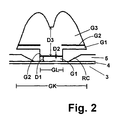
- Essential for the present invention is the layer structure of the metallic gate electrode of the example of a first layer G1 on the semiconductor material of the semiconductor layer 4 in the access trench RC, a second layer G2 on the first layer and a further layer G3 on the second layer G2.
- the layer sequence can be found both in the gate base above the semiconductor material in the recess trench and in the gate head above the protective layer laterally of the opening MF.
- the proportions of the individual layers and / or the control electrode in the figures are not strictly to scale.
- the layer G1 consists of aluminum, which in a particularly advantageous manner forms an interface with the material of the semiconductor layer 4 and can form a Schottky diode with it in particular.
- the layer 1 is deposited with a layer thickness D1, which advantageously is not greater than 1.5 times the gate length GL, in particular not greater than the gate length GL of the control electrode, see FIG. 2.
- the layer G1 is also located laterally of the opening MF and within the opening MK on the upper surface of the protective layer 6 with a width GK of the gate head parallel to the direction of the gate length.
- the gate length GL is advantageously less than 300 nm, in particular in a range between 20 nm and 300 nm.
- the width GK of the gate head is greater than the gate length GL and is preferably at least 1.5 times that Gate length GL.
- the width GK of the gate head is between 400 nm and 650 nm.
- the thickness D1 of the first layer G1 perpendicular to the plane of the semiconductor layers is advantageously between 10 nm and 100 nm.
- the layer thickness D1 of the first layer is advantageously at least 50%, in particular at least 65%, preferably at least 75% of the depth of the recession trench RC under the protective layer 6.
- the depth of the trench is at least approximately equal to the layer thickness of the contact layer 5.
- a second layer G2 of a second metal is deposited through the opening MF and through the opening MK.
- the second metal is different from aluminum and advantageously has the property of being alloyable with Al and limiting the grain size growth of aluminum in the layer G1 during later temperature treatment and / or operation by electromigration.
- Pt, Ni or, more particularly, Ti are suitable.
- the grain growth is limited by the fact that grains in the aluminum layer G1 grow simultaneously on all sides and stopping grain size growth at the layer boundary from G1 to G2 substantially also stops grain size growth transversely to the layer boundary level entails. Of particular importance is thus in particular the small layer thickness of the layer G 1.
- the second layer thickness D2 of the second layer G2 is advantageously less than 10 nm, in particular less than 5 nm, preferably less than 2.5 nm.
- On the second layer G2 further gate metal is deposited in at least one further layer, preferably exactly one further layer G3 , The deposition of the further gate metal in the layer G3 takes place in a layer thickness D3, which is advantageously greater than the sum of the first and second layer thicknesses, G1 and G2.
- the gate head advantageously consists predominantly of the further gate metal in the further layer G3.
- the further layer G3 is advantageously made of aluminum as a further gate metal. This advantageously has a very low specific electrical resistance.
- grain size growth also occurs in the aluminum of the further layer G3.
- no measures are required or provided to limit the grain size growth. Larger grain sizes can be favorable with respect to the electrical resistance of the gate, which is perpendicular to the plane of the drawing.
- an average grain size of the aluminum is advantageously obtained which is smaller than the average grain size of the aluminum in the further layer G3 and advantageously less than 50%, in particular less than 20%, of the mean grain size of the aluminum in the further layer G3.
- alloying also occurs at the interfaces of the second layer G2 to the first layer G1 and the third layer G1 of the different metals.
- An alloying zone forming in the first layer advantageously does not reach the semiconductor layer 4 and is sufficiently spaced therefrom, so that the properties of the Schottky junction between the first layer G1 of the control electrode and the semiconductor layer 4 are not impaired by the alloy.
Landscapes
- Junction Field-Effect Transistors (AREA)
- Electrodes Of Semiconductors (AREA)
Applications Claiming Priority (1)
| Application Number | Priority Date | Filing Date | Title |
|---|---|---|---|
| DE102006012369A DE102006012369A1 (de) | 2006-03-17 | 2006-03-17 | Verfahren zur Herstellung eines Halbleiterbauelements mit einer metallischen Steuerelektrode und Halbleiterbauelement |
Publications (3)
| Publication Number | Publication Date |
|---|---|
| EP1835528A2 true EP1835528A2 (fr) | 2007-09-19 |
| EP1835528A3 EP1835528A3 (fr) | 2009-10-21 |
| EP1835528B1 EP1835528B1 (fr) | 2012-02-01 |
Family
ID=38162142
Family Applications (1)
| Application Number | Title | Priority Date | Filing Date |
|---|---|---|---|
| EP06007759A Expired - Lifetime EP1835528B1 (fr) | 2006-03-17 | 2006-04-13 | Procédé de fabrication d'un dispositif semi-conducteur avec une grille métallique et dispositif semi-conducteur |
Country Status (8)
| Country | Link |
|---|---|
| US (1) | US7573122B2 (fr) |
| EP (1) | EP1835528B1 (fr) |
| JP (1) | JP5348847B2 (fr) |
| CN (1) | CN101043003B (fr) |
| AT (1) | ATE544177T1 (fr) |
| CA (1) | CA2579325C (fr) |
| DE (1) | DE102006012369A1 (fr) |
| TW (1) | TWI350560B (fr) |
Families Citing this family (4)
| Publication number | Priority date | Publication date | Assignee | Title |
|---|---|---|---|---|
| US8502272B2 (en) * | 2007-05-16 | 2013-08-06 | Avago Technologies General Ip (Singapore) Pte. Ltd. | Metal-oxide-semiconductor high electron mobility transistors and methods of fabrication |
| KR102150850B1 (ko) * | 2017-02-27 | 2020-09-02 | 미쓰비시덴키 가부시키가이샤 | 반도체 장치 및 그 제조 방법 |
| CN113793803B (zh) * | 2021-08-19 | 2024-10-25 | 联芯集成电路制造(厦门)有限公司 | 铝金属栅极的制作方法 |
| US12520533B2 (en) * | 2021-10-27 | 2026-01-06 | Win Semiconductors Corp. | Transistor device and gate structure |
Citations (2)
| Publication number | Priority date | Publication date | Assignee | Title |
|---|---|---|---|---|
| US4679311A (en) | 1985-12-12 | 1987-07-14 | Allied Corporation | Method of fabricating self-aligned field-effect transistor having t-shaped gate electrode, sub-micron gate length and variable drain to gate spacing |
| US6011281A (en) | 1997-12-02 | 2000-01-04 | Fujitsu Quantum Devices Limited | Semiconductor device having an ohmic contact and a Schottky contact, with a barrier layer interposed between the ohmic contact and the Schottky contact |
Family Cites Families (15)
| Publication number | Priority date | Publication date | Assignee | Title |
|---|---|---|---|---|
| JPS59119868A (ja) * | 1982-12-27 | 1984-07-11 | Nippon Telegr & Teleph Corp <Ntt> | 半導体装置 |
| JPH05335348A (ja) * | 1992-05-29 | 1993-12-17 | Toshiba Corp | 半導体装置 |
| JPH08139106A (ja) * | 1994-11-11 | 1996-05-31 | Hitachi Ltd | 電界効果型化合物半導体装置 |
| JPH10107300A (ja) * | 1996-10-03 | 1998-04-24 | Hitachi Ltd | 半導体装置 |
| JPH11154678A (ja) * | 1997-11-20 | 1999-06-08 | Nec Corp | 半導体装置およびその製造方法 |
| JP3416532B2 (ja) * | 1998-06-15 | 2003-06-16 | 富士通カンタムデバイス株式会社 | 化合物半導体装置及びその製造方法 |
| JP4584379B2 (ja) * | 1999-07-16 | 2010-11-17 | 三菱電機株式会社 | 半導体装置の製造方法 |
| US6686616B1 (en) * | 2000-05-10 | 2004-02-03 | Cree, Inc. | Silicon carbide metal-semiconductor field effect transistors |
| US6906350B2 (en) * | 2001-10-24 | 2005-06-14 | Cree, Inc. | Delta doped silicon carbide metal-semiconductor field effect transistors having a gate disposed in a double recess structure |
| JP4865189B2 (ja) * | 2002-02-21 | 2012-02-01 | 古河電気工業株式会社 | GaN系電界効果トランジスタ |
| DE10304722A1 (de) | 2002-05-11 | 2004-08-19 | United Monolithic Semiconductors Gmbh | Verfahren zur Herstellung eines Halbleiterbauelements |
| JP2004055677A (ja) * | 2002-07-17 | 2004-02-19 | Communication Research Laboratory | 電界効果トランジスタのゲート電極とその作製方法 |
| JP3960957B2 (ja) * | 2003-09-05 | 2007-08-15 | 古河電気工業株式会社 | 半導体電子デバイス |
| US7129182B2 (en) * | 2003-11-06 | 2006-10-31 | Intel Corporation | Method for etching a thin metal layer |
| US7253015B2 (en) * | 2004-02-17 | 2007-08-07 | Velox Semiconductor Corporation | Low doped layer for nitride-based semiconductor device |
-
2006
- 2006-03-17 DE DE102006012369A patent/DE102006012369A1/de not_active Withdrawn
- 2006-04-13 AT AT06007759T patent/ATE544177T1/de active
- 2006-04-13 EP EP06007759A patent/EP1835528B1/fr not_active Expired - Lifetime
- 2006-11-28 US US11/605,020 patent/US7573122B2/en active Active
-
2007
- 2007-02-20 CA CA 2579325 patent/CA2579325C/fr active Active
- 2007-03-14 CN CN2007100886686A patent/CN101043003B/zh active Active
- 2007-03-15 TW TW096108971A patent/TWI350560B/zh active
- 2007-03-19 JP JP2007070894A patent/JP5348847B2/ja active Active
Patent Citations (2)
| Publication number | Priority date | Publication date | Assignee | Title |
|---|---|---|---|---|
| US4679311A (en) | 1985-12-12 | 1987-07-14 | Allied Corporation | Method of fabricating self-aligned field-effect transistor having t-shaped gate electrode, sub-micron gate length and variable drain to gate spacing |
| US6011281A (en) | 1997-12-02 | 2000-01-04 | Fujitsu Quantum Devices Limited | Semiconductor device having an ohmic contact and a Schottky contact, with a barrier layer interposed between the ohmic contact and the Schottky contact |
Also Published As
| Publication number | Publication date |
|---|---|
| TWI350560B (en) | 2011-10-11 |
| JP5348847B2 (ja) | 2013-11-20 |
| TW200737318A (en) | 2007-10-01 |
| DE102006012369A1 (de) | 2007-09-20 |
| EP1835528B1 (fr) | 2012-02-01 |
| JP2007251180A (ja) | 2007-09-27 |
| ATE544177T1 (de) | 2012-02-15 |
| EP1835528A3 (fr) | 2009-10-21 |
| CN101043003A (zh) | 2007-09-26 |
| US7573122B2 (en) | 2009-08-11 |
| CA2579325C (fr) | 2015-04-28 |
| US20070218642A1 (en) | 2007-09-20 |
| CN101043003B (zh) | 2011-09-21 |
| CA2579325A1 (fr) | 2007-09-17 |
Similar Documents
| Publication | Publication Date | Title |
|---|---|---|
| DE112010001555B4 (de) | GaN-HEMT vom Anreicherungstyp und Verfahren zu seiner Herstellung | |
| DE69835986T2 (de) | Elektrode eines halbleitenden Nitrids vom N-Typ, ein Halbleiterbauelement mit einer solchen Elektrode und ein Herstellungsverfahren | |
| DE112010001589B4 (de) | Kompensierter GATE-MISFET | |
| DE3939319C2 (de) | Verfahren zum Herstellen eines asymmetrischen Feldeffekttransistors | |
| DE112007000697B4 (de) | Leistungshalbleitervorrichtung | |
| DE112018007009T5 (de) | Halbleitervorrichtung und Herstellungsverfahren für diese | |
| DE112006000133T5 (de) | Eine dielektrische Schicht mit hoher dielektrischer Konstante nutzender Quantentopf-Transistor | |
| DE112010004400B4 (de) | Bildung von Nickelsilicid mit Gestaffelter PT-Zusammensetzung | |
| DE112018003057T5 (de) | Gan-transistor im anreicherungsmodus mit selektiven und nicht selektiven ätzschichten für verbesserte gleichförmigkeit der gan-spacerdicke | |
| EP0012955A2 (fr) | Solution pour l'attaque d'oxydes de silicium sur un substrat et procédé d'attaque utilisant la solution | |
| DE112017007040T5 (de) | Halbleitereinheit | |
| EP0002731A1 (fr) | Structure à film mince pour une disposition de contact et procédé pour sa fabrication | |
| DE102008060704A1 (de) | Zusammengesetzter Passivierungsprozess für Nitrid-Feldeffekttransistoren | |
| EP1858064B1 (fr) | Procédé de fabrication d'un élément semi-conducteur doté d'une électrode porte métallique agencée dans une double structure à tranchée | |
| DE2805442A1 (de) | Verfahren zum herstellen eines schottky-sperrschicht-halbleiterbauelementes | |
| DE102021115509A1 (de) | Galliumnitrid-basierte vorrichtung mit stufenartiger feldplatte und verfahren zu deren herstellung | |
| DE3784761T2 (de) | Verfahren zur herstellung eines mesfets. | |
| DE102013202972B4 (de) | Anreicherungsbetrieb einer GaN-HEMT-Vorrichtung mit einem GATE-Abstandshalter sowie Verfahren zu deren Herstellung | |
| EP1835528B1 (fr) | Procédé de fabrication d'un dispositif semi-conducteur avec une grille métallique et dispositif semi-conducteur | |
| EP1090415B1 (fr) | Dispositif a semi-conducteur avec contact ohmique et procede de realisation d'un contact sur un dispositif a semi-conducteur | |
| DE102017108568A1 (de) | kohlenstoffbasierte Kontaktstruktur für ein Siliziumkarbid-Bauelement | |
| DE69215956T2 (de) | Verfahren zum Herstellen eines Kontakts auf einem Halbleiterbauelement | |
| DE69322223T2 (de) | Kontaktierungsverfahren für eine Halbleitervorrichtung | |
| DE3538855A1 (de) | Verfahren zur herstellung einer halbleitervorrichtung | |
| EP0823728A2 (fr) | Méthode de fabrication d'un transistor à effet de champ |
Legal Events
| Date | Code | Title | Description |
|---|---|---|---|
| PUAI | Public reference made under article 153(3) epc to a published international application that has entered the european phase |
Free format text: ORIGINAL CODE: 0009012 |
|
| AK | Designated contracting states |
Kind code of ref document: A2 Designated state(s): AT BE BG CH CY CZ DE DK EE ES FI FR GB GR HU IE IS IT LI LT LU LV MC NL PL PT RO SE SI SK TR |
|
| AX | Request for extension of the european patent |
Extension state: AL BA HR MK YU |
|
| PUAL | Search report despatched |
Free format text: ORIGINAL CODE: 0009013 |
|
| AK | Designated contracting states |
Kind code of ref document: A3 Designated state(s): AT BE BG CH CY CZ DE DK EE ES FI FR GB GR HU IE IS IT LI LT LU LV MC NL PL PT RO SE SI SK TR |
|
| AX | Request for extension of the european patent |
Extension state: AL BA HR MK YU |
|
| 17P | Request for examination filed |
Effective date: 20100421 |
|
| AKX | Designation fees paid |
Designated state(s): AT BE BG CH CY CZ DE DK EE ES FI FR GB GR HU IE IS IT LI LT LU LV MC NL PL PT RO SE SI SK TR |
|
| GRAP | Despatch of communication of intention to grant a patent |
Free format text: ORIGINAL CODE: EPIDOSNIGR1 |
|
| GRAS | Grant fee paid |
Free format text: ORIGINAL CODE: EPIDOSNIGR3 |
|
| GRAA | (expected) grant |
Free format text: ORIGINAL CODE: 0009210 |
|
| AK | Designated contracting states |
Kind code of ref document: B1 Designated state(s): AT BE BG CH CY CZ DE DK EE ES FI FR GB GR HU IE IS IT LI LT LU LV MC NL PL PT RO SE SI SK TR |
|
| REG | Reference to a national code |
Ref country code: GB Ref legal event code: FG4D Free format text: NOT ENGLISH |
|
| REG | Reference to a national code |
Ref country code: AT Ref legal event code: REF Ref document number: 544177 Country of ref document: AT Kind code of ref document: T Effective date: 20120215 Ref country code: CH Ref legal event code: EP |
|
| REG | Reference to a national code |
Ref country code: DE Ref legal event code: R096 Ref document number: 502006010932 Country of ref document: DE Effective date: 20120329 |
|
| REG | Reference to a national code |
Ref country code: NL Ref legal event code: T3 |
|
| LTIE | Lt: invalidation of european patent or patent extension |
Effective date: 20120201 |
|
| PG25 | Lapsed in a contracting state [announced via postgrant information from national office to epo] |
Ref country code: LT Free format text: LAPSE BECAUSE OF FAILURE TO SUBMIT A TRANSLATION OF THE DESCRIPTION OR TO PAY THE FEE WITHIN THE PRESCRIBED TIME-LIMIT Effective date: 20120201 Ref country code: IS Free format text: LAPSE BECAUSE OF FAILURE TO SUBMIT A TRANSLATION OF THE DESCRIPTION OR TO PAY THE FEE WITHIN THE PRESCRIBED TIME-LIMIT Effective date: 20120601 |
|
| REG | Reference to a national code |
Ref country code: IE Ref legal event code: FD4D |
|
| PG25 | Lapsed in a contracting state [announced via postgrant information from national office to epo] |
Ref country code: FI Free format text: LAPSE BECAUSE OF FAILURE TO SUBMIT A TRANSLATION OF THE DESCRIPTION OR TO PAY THE FEE WITHIN THE PRESCRIBED TIME-LIMIT Effective date: 20120201 Ref country code: PL Free format text: LAPSE BECAUSE OF FAILURE TO SUBMIT A TRANSLATION OF THE DESCRIPTION OR TO PAY THE FEE WITHIN THE PRESCRIBED TIME-LIMIT Effective date: 20120201 Ref country code: PT Free format text: LAPSE BECAUSE OF FAILURE TO SUBMIT A TRANSLATION OF THE DESCRIPTION OR TO PAY THE FEE WITHIN THE PRESCRIBED TIME-LIMIT Effective date: 20120601 Ref country code: LV Free format text: LAPSE BECAUSE OF FAILURE TO SUBMIT A TRANSLATION OF THE DESCRIPTION OR TO PAY THE FEE WITHIN THE PRESCRIBED TIME-LIMIT Effective date: 20120201 Ref country code: GR Free format text: LAPSE BECAUSE OF FAILURE TO SUBMIT A TRANSLATION OF THE DESCRIPTION OR TO PAY THE FEE WITHIN THE PRESCRIBED TIME-LIMIT Effective date: 20120502 |
|
| PG25 | Lapsed in a contracting state [announced via postgrant information from national office to epo] |
Ref country code: CY Free format text: LAPSE BECAUSE OF FAILURE TO SUBMIT A TRANSLATION OF THE DESCRIPTION OR TO PAY THE FEE WITHIN THE PRESCRIBED TIME-LIMIT Effective date: 20120201 |
|
| PG25 | Lapsed in a contracting state [announced via postgrant information from national office to epo] |
Ref country code: IE Free format text: LAPSE BECAUSE OF FAILURE TO SUBMIT A TRANSLATION OF THE DESCRIPTION OR TO PAY THE FEE WITHIN THE PRESCRIBED TIME-LIMIT Effective date: 20120201 Ref country code: SI Free format text: LAPSE BECAUSE OF FAILURE TO SUBMIT A TRANSLATION OF THE DESCRIPTION OR TO PAY THE FEE WITHIN THE PRESCRIBED TIME-LIMIT Effective date: 20120201 Ref country code: EE Free format text: LAPSE BECAUSE OF FAILURE TO SUBMIT A TRANSLATION OF THE DESCRIPTION OR TO PAY THE FEE WITHIN THE PRESCRIBED TIME-LIMIT Effective date: 20120201 Ref country code: CZ Free format text: LAPSE BECAUSE OF FAILURE TO SUBMIT A TRANSLATION OF THE DESCRIPTION OR TO PAY THE FEE WITHIN THE PRESCRIBED TIME-LIMIT Effective date: 20120201 Ref country code: RO Free format text: LAPSE BECAUSE OF FAILURE TO SUBMIT A TRANSLATION OF THE DESCRIPTION OR TO PAY THE FEE WITHIN THE PRESCRIBED TIME-LIMIT Effective date: 20120201 Ref country code: SE Free format text: LAPSE BECAUSE OF FAILURE TO SUBMIT A TRANSLATION OF THE DESCRIPTION OR TO PAY THE FEE WITHIN THE PRESCRIBED TIME-LIMIT Effective date: 20120201 Ref country code: DK Free format text: LAPSE BECAUSE OF FAILURE TO SUBMIT A TRANSLATION OF THE DESCRIPTION OR TO PAY THE FEE WITHIN THE PRESCRIBED TIME-LIMIT Effective date: 20120201 |
|
| PG25 | Lapsed in a contracting state [announced via postgrant information from national office to epo] |
Ref country code: MC Free format text: LAPSE BECAUSE OF NON-PAYMENT OF DUE FEES Effective date: 20120430 Ref country code: SK Free format text: LAPSE BECAUSE OF FAILURE TO SUBMIT A TRANSLATION OF THE DESCRIPTION OR TO PAY THE FEE WITHIN THE PRESCRIBED TIME-LIMIT Effective date: 20120201 |
|
| REG | Reference to a national code |
Ref country code: CH Ref legal event code: PL |
|
| PLBE | No opposition filed within time limit |
Free format text: ORIGINAL CODE: 0009261 |
|
| STAA | Information on the status of an ep patent application or granted ep patent |
Free format text: STATUS: NO OPPOSITION FILED WITHIN TIME LIMIT |
|
| 26N | No opposition filed |
Effective date: 20121105 |
|
| PG25 | Lapsed in a contracting state [announced via postgrant information from national office to epo] |
Ref country code: LI Free format text: LAPSE BECAUSE OF NON-PAYMENT OF DUE FEES Effective date: 20120430 Ref country code: CH Free format text: LAPSE BECAUSE OF NON-PAYMENT OF DUE FEES Effective date: 20120430 |
|
| REG | Reference to a national code |
Ref country code: DE Ref legal event code: R097 Ref document number: 502006010932 Country of ref document: DE Effective date: 20121105 |
|
| PG25 | Lapsed in a contracting state [announced via postgrant information from national office to epo] |
Ref country code: ES Free format text: LAPSE BECAUSE OF FAILURE TO SUBMIT A TRANSLATION OF THE DESCRIPTION OR TO PAY THE FEE WITHIN THE PRESCRIBED TIME-LIMIT Effective date: 20120512 |
|
| REG | Reference to a national code |
Ref country code: AT Ref legal event code: MM01 Ref document number: 544177 Country of ref document: AT Kind code of ref document: T Effective date: 20120413 |
|
| PG25 | Lapsed in a contracting state [announced via postgrant information from national office to epo] |
Ref country code: AT Free format text: LAPSE BECAUSE OF NON-PAYMENT OF DUE FEES Effective date: 20120413 Ref country code: BG Free format text: LAPSE BECAUSE OF FAILURE TO SUBMIT A TRANSLATION OF THE DESCRIPTION OR TO PAY THE FEE WITHIN THE PRESCRIBED TIME-LIMIT Effective date: 20120501 |
|
| PG25 | Lapsed in a contracting state [announced via postgrant information from national office to epo] |
Ref country code: TR Free format text: LAPSE BECAUSE OF FAILURE TO SUBMIT A TRANSLATION OF THE DESCRIPTION OR TO PAY THE FEE WITHIN THE PRESCRIBED TIME-LIMIT Effective date: 20120201 |
|
| PG25 | Lapsed in a contracting state [announced via postgrant information from national office to epo] |
Ref country code: LU Free format text: LAPSE BECAUSE OF NON-PAYMENT OF DUE FEES Effective date: 20120413 |
|
| REG | Reference to a national code |
Ref country code: DE Ref legal event code: R082 Ref document number: 502006010932 Country of ref document: DE Representative=s name: BAUR & WEBER PATENTANWAELTE PARTG MBB, DE Ref country code: DE Ref legal event code: R082 Ref document number: 502006010932 Country of ref document: DE Representative=s name: BAUR & WEBER PATENTANWAELTE, DE |
|
| PG25 | Lapsed in a contracting state [announced via postgrant information from national office to epo] |
Ref country code: HU Free format text: LAPSE BECAUSE OF FAILURE TO SUBMIT A TRANSLATION OF THE DESCRIPTION OR TO PAY THE FEE WITHIN THE PRESCRIBED TIME-LIMIT Effective date: 20060413 |
|
| REG | Reference to a national code |
Ref country code: FR Ref legal event code: PLFP Year of fee payment: 11 |
|
| REG | Reference to a national code |
Ref country code: FR Ref legal event code: PLFP Year of fee payment: 12 |
|
| REG | Reference to a national code |
Ref country code: FR Ref legal event code: PLFP Year of fee payment: 13 |
|
| REG | Reference to a national code |
Ref country code: DE Ref legal event code: R079 Ref document number: 502006010932 Country of ref document: DE Free format text: PREVIOUS MAIN CLASS: H01L0021280000 Ipc: H10D0064010000 |
|
| PGFP | Annual fee paid to national office [announced via postgrant information from national office to epo] |
Ref country code: NL Payment date: 20250422 Year of fee payment: 20 |
|
| PGFP | Annual fee paid to national office [announced via postgrant information from national office to epo] |
Ref country code: DE Payment date: 20250430 Year of fee payment: 20 |
|
| PGFP | Annual fee paid to national office [announced via postgrant information from national office to epo] |
Ref country code: GB Payment date: 20250423 Year of fee payment: 20 |
|
| PGFP | Annual fee paid to national office [announced via postgrant information from national office to epo] |
Ref country code: BE Payment date: 20250422 Year of fee payment: 20 Ref country code: IT Payment date: 20250430 Year of fee payment: 20 |
|
| PGFP | Annual fee paid to national office [announced via postgrant information from national office to epo] |
Ref country code: FR Payment date: 20250425 Year of fee payment: 20 |
|
| REG | Reference to a national code |
Ref country code: DE Ref legal event code: R071 Ref document number: 502006010932 Country of ref document: DE |
|
| REG | Reference to a national code |
Ref country code: NL Ref legal event code: MK Effective date: 20260412 |