EP1840957A1 - Procédé de production de plaquette simox - Google Patents
Procédé de production de plaquette simox Download PDFInfo
- Publication number
- EP1840957A1 EP1840957A1 EP07006289A EP07006289A EP1840957A1 EP 1840957 A1 EP1840957 A1 EP 1840957A1 EP 07006289 A EP07006289 A EP 07006289A EP 07006289 A EP07006289 A EP 07006289A EP 1840957 A1 EP1840957 A1 EP 1840957A1
- Authority
- EP
- European Patent Office
- Prior art keywords
- oxide film
- ion implantation
- oxygen ion
- simox
- producing
- Prior art date
- Legal status (The legal status is an assumption and is not a legal conclusion. Google has not performed a legal analysis and makes no representation as to the accuracy of the status listed.)
- Withdrawn
Links
Images

Classifications
-
- H—ELECTRICITY
- H10—SEMICONDUCTOR DEVICES; ELECTRIC SOLID-STATE DEVICES NOT OTHERWISE PROVIDED FOR
- H10P—GENERIC PROCESSES OR APPARATUS FOR THE MANUFACTURE OR TREATMENT OF DEVICES COVERED BY CLASS H10
- H10P95/00—Generic processes or apparatus for manufacture or treatments not covered by the other groups of this subclass
-
- H—ELECTRICITY
- H10—SEMICONDUCTOR DEVICES; ELECTRIC SOLID-STATE DEVICES NOT OTHERWISE PROVIDED FOR
- H10P—GENERIC PROCESSES OR APPARATUS FOR THE MANUFACTURE OR TREATMENT OF DEVICES COVERED BY CLASS H10
- H10P30/00—Ion implantation into wafers, substrates or parts of devices
- H10P30/20—Ion implantation into wafers, substrates or parts of devices into semiconductor materials, e.g. for doping
- H10P30/208—Ion implantation into wafers, substrates or parts of devices into semiconductor materials, e.g. for doping of electrically inactive species
- H10P30/209—Ion implantation into wafers, substrates or parts of devices into semiconductor materials, e.g. for doping of electrically inactive species in silicon to make buried insulating layers
-
- H—ELECTRICITY
- H10—SEMICONDUCTOR DEVICES; ELECTRIC SOLID-STATE DEVICES NOT OTHERWISE PROVIDED FOR
- H10P—GENERIC PROCESSES OR APPARATUS FOR THE MANUFACTURE OR TREATMENT OF DEVICES COVERED BY CLASS H10
- H10P14/00—Formation of materials, e.g. in the shape of layers or pillars
- H10P14/20—Formation of materials, e.g. in the shape of layers or pillars of semiconductor materials
-
- H—ELECTRICITY
- H10—SEMICONDUCTOR DEVICES; ELECTRIC SOLID-STATE DEVICES NOT OTHERWISE PROVIDED FOR
- H10P—GENERIC PROCESSES OR APPARATUS FOR THE MANUFACTURE OR TREATMENT OF DEVICES COVERED BY CLASS H10
- H10P90/00—Preparation of wafers not covered by a single main group of this subclass, e.g. wafer reinforcement
- H10P90/19—Preparing inhomogeneous wafers
- H10P90/1904—Preparing vertically inhomogeneous wafers
- H10P90/1906—Preparing SOI wafers
- H10P90/1908—Preparing SOI wafers using silicon implanted buried insulating layers, e.g. oxide layers [SIMOX]
-
- H—ELECTRICITY
- H10—SEMICONDUCTOR DEVICES; ELECTRIC SOLID-STATE DEVICES NOT OTHERWISE PROVIDED FOR
- H10W—GENERIC PACKAGES, INTERCONNECTIONS, CONNECTORS OR OTHER CONSTRUCTIONAL DETAILS OF DEVICES COVERED BY CLASS H10
- H10W10/00—Isolation regions in semiconductor bodies between components of integrated devices
- H10W10/10—Isolation regions comprising dielectric materials
- H10W10/181—Semiconductor-on-insulator [SOI] isolation regions, e.g. buried oxide regions of SOI wafers
Definitions
- the annealing is carried out in an Ar atmosphere containing 0.5-2% of oxygen for about 5-10 hours after the ITOX step in order to decrease an oxygen content in SOl layer.
- the SIMOX process roughly consists of an implantation step of implanting the oxygen ion at an energy of about 150 keV or more and at a dose of about 1.5x10 17 -1x10 18 cm -2 and a high-temperate annealing step of bringing back the damage produced by the implanted oxygen ion to form a flat buried oxide film (BOX).
- the oxygen ion is implanted into a bare silicon wafer (having no oxide film or the like) and the bare silicon is annealed at a high temperature to form the buried oxide film (BOX).
- an object of the invention to advantageously solve the aforementioned problems and to propose a method of producing SIMOX wafer in which the adhesion of particles onto the silicon surface is effectively suppressed not only at the oxygen ion implantation step but also at the high-temperature annealing step to largely reduce the occurrence of surface defect resulted from these particles as compared with the conventional techniques.
- the direct contact of the particles adhered onto the wafer with the silicon surface can be prevented effectively not only at the oxygen ion implantation step in SIMOX process but also at the high-temperature annealing step, and as a result, the occurrence of surface defect resulted from the particles can be largely reduced as compared with the conventional technique.
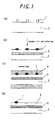
- FIG. 1 is a schematic view illustrating a behavior of particles in SIMOX process according to the conventional technique.
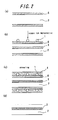
- the screen oxide is left up to the high-temperature annealing step without the complete removal after the oxygen ion implantation, it effectively serves as a protection film to the particles in the high-temperature annealing process. Even in the high-temperature annealing process, it is considered that the particles particularly adhered onto the bare silicon surface at an initial process stage not forming a surface oxide film are baked on the surface in the subsequent high-temperature annealing, which is high in the possibility of causing the surface defect in a final product. Moreover, all of the screen oxide and an oxide film formed in the annealing are finally removed, so that the particles adhered in the annealing can be effectively removed together with these oxide films.
- the silicon surface is covered with an insulating film, so that there is feared a problem on a charge-up in the ion implantation.
- a portion of holding the wafer with a holder corresponds to an outer peripheral edge portion of the wafer, so that it is desirable that only the insulating film is removed from the outer peripheral edge portion by a distance of several mm by etching this portion with a solution of HF or the like. That is, as shown in FIG. 3, it is preferable that the screen oxide 6 is removed from the outer periphery by only several mm over a full periphery of the wafer 2. In this way, electric charges flow effectively from a contact pin at the oxygen ion implantation step, so that the problem on the charge-up in the ion implantation is overcome.
- FIG. 4 For reference, a typical flow chart of SIMOX process according to the invention is shown in FIG. 4.
- the oxygen ion implantation is first carried out under conditions of an acceleration energy: 170 keV, a dose: 2.5x10 17 cm -2 and a substrate temperature: 400°C and thereafter the ion implantation is carried out at room temperature and a dose of 2.5x10 15 cm -2 . Then, ITOX process is conducted at 1320°C for 10 hours and the annealing is carried out in an Ar atmosphere (oxygen content: 4%) at 1350°C for 10-20 hours. With respect to the thus obtained wafer is examined the particle defect to obtain a result as shown in Table 1.
- Nos. 1-5 are comparative examples according to the conventional method
- Nos. 6-10 are invention examples in which a screen oxide is formed on a surface of a wafer prior to the oxygen ion implantation according to the invention and then the ion implantation is conducted through the screen oxide.
- a part or a whole of the screen oxide is removed by etching after the ion implantation.
- the thickness of the screen oxide and the removing ratio of the screen oxide after the oxygen ion implantation are shown in Table 1.
- the particle level can be largely reduced by using SIMOX process according to the invention.
- the invention develops the effect that the final particle level on SOI surface is largely improved. Also, when the high-temperature annealing is carried out at a state of existing the screen oxide on the rear face of the wafer, the bare rear face is not directly contacted with the wafer holder in the high-temperature annealing, so that there is obtained an additional effect that the occurrence of flaw feared on the rear face of the wafer is largely decreased.
Landscapes
- Element Separation (AREA)
- Formation Of Insulating Films (AREA)
- Physical Vapour Deposition (AREA)
Applications Claiming Priority (1)
| Application Number | Priority Date | Filing Date | Title |
|---|---|---|---|
| JP2006085340A JP5157075B2 (ja) | 2006-03-27 | 2006-03-27 | Simoxウェーハの製造方法 |
Publications (1)
| Publication Number | Publication Date |
|---|---|
| EP1840957A1 true EP1840957A1 (fr) | 2007-10-03 |
Family
ID=38197993
Family Applications (1)
| Application Number | Title | Priority Date | Filing Date |
|---|---|---|---|
| EP07006289A Withdrawn EP1840957A1 (fr) | 2006-03-27 | 2007-03-27 | Procédé de production de plaquette simox |
Country Status (6)
| Country | Link |
|---|---|
| US (1) | US20070224773A1 (fr) |
| EP (1) | EP1840957A1 (fr) |
| JP (1) | JP5157075B2 (fr) |
| KR (1) | KR100878732B1 (fr) |
| SG (2) | SG136099A1 (fr) |
| TW (1) | TWI345286B (fr) |
Cited By (1)
| Publication number | Priority date | Publication date | Assignee | Title |
|---|---|---|---|---|
| US8778717B2 (en) | 2010-03-17 | 2014-07-15 | Taiwan Semiconductor Manufacturing Company, Ltd. | Local oxidation of silicon processes with reduced lateral oxidation |
Families Citing this family (3)
| Publication number | Priority date | Publication date | Assignee | Title |
|---|---|---|---|---|
| US8858818B2 (en) * | 2010-09-30 | 2014-10-14 | Suvolta, Inc. | Method for minimizing defects in a semiconductor substrate due to ion implantation |
| US8778786B1 (en) | 2012-05-29 | 2014-07-15 | Suvolta, Inc. | Method for substrate preservation during transistor fabrication |
| JP6502198B2 (ja) * | 2015-07-02 | 2019-04-17 | 東京エレクトロン株式会社 | 基板処理方法および記憶媒体 |
Citations (4)
| Publication number | Priority date | Publication date | Assignee | Title |
|---|---|---|---|---|
| US4786608A (en) * | 1986-12-30 | 1988-11-22 | Harris Corp. | Technique for forming electric field shielding layer in oxygen-implanted silicon substrate |
| US5364800A (en) * | 1993-06-24 | 1994-11-15 | Texas Instruments Incorporated | Varying the thickness of the surface silicon layer in a silicon-on-insulator substrate |
| JPH1041241A (ja) * | 1996-07-26 | 1998-02-13 | Sharp Corp | 半導体装置の製造方法 |
| EP0966034A1 (fr) * | 1998-06-18 | 1999-12-22 | Canon Kabushiki Kaisha | Méthode de fabrication d'un substrat silicium sur isolant |
Family Cites Families (8)
| Publication number | Priority date | Publication date | Assignee | Title |
|---|---|---|---|---|
| FR2528018A1 (fr) * | 1982-06-07 | 1983-12-09 | Cuir Sa | Taquets de positionnement de produits en feuille |
| JPH04737A (ja) * | 1990-04-17 | 1992-01-06 | Fujitsu Ltd | 半導体装置の製造方法 |
| JPH07193204A (ja) * | 1993-12-27 | 1995-07-28 | Nippon Steel Corp | 半導体基板の製造方法 |
| JP3036619B2 (ja) * | 1994-03-23 | 2000-04-24 | コマツ電子金属株式会社 | Soi基板の製造方法およびsoi基板 |
| JPH07335906A (ja) * | 1994-06-14 | 1995-12-22 | Semiconductor Energy Lab Co Ltd | 薄膜状半導体装置およびその作製方法 |
| KR0143344B1 (ko) * | 1994-11-02 | 1998-08-17 | 김주용 | 온도의 변화에 대하여 보상 기능이 있는 기준전압 발생기 |
| US5930643A (en) * | 1997-12-22 | 1999-07-27 | International Business Machines Corporation | Defect induced buried oxide (DIBOX) for throughput SOI |
| TW587332B (en) * | 2000-01-07 | 2004-05-11 | Canon Kk | Semiconductor substrate and process for its production |
-
2006
- 2006-03-27 JP JP2006085340A patent/JP5157075B2/ja not_active Expired - Fee Related
-
2007
- 2007-03-27 TW TW096110633A patent/TWI345286B/zh not_active IP Right Cessation
- 2007-03-27 US US11/729,229 patent/US20070224773A1/en not_active Abandoned
- 2007-03-27 SG SG200702274-2A patent/SG136099A1/en unknown
- 2007-03-27 SG SG200906432-0A patent/SG155989A1/en unknown
- 2007-03-27 EP EP07006289A patent/EP1840957A1/fr not_active Withdrawn
- 2007-03-27 KR KR1020070029964A patent/KR100878732B1/ko not_active Expired - Fee Related
Patent Citations (4)
| Publication number | Priority date | Publication date | Assignee | Title |
|---|---|---|---|---|
| US4786608A (en) * | 1986-12-30 | 1988-11-22 | Harris Corp. | Technique for forming electric field shielding layer in oxygen-implanted silicon substrate |
| US5364800A (en) * | 1993-06-24 | 1994-11-15 | Texas Instruments Incorporated | Varying the thickness of the surface silicon layer in a silicon-on-insulator substrate |
| JPH1041241A (ja) * | 1996-07-26 | 1998-02-13 | Sharp Corp | 半導体装置の製造方法 |
| EP0966034A1 (fr) * | 1998-06-18 | 1999-12-22 | Canon Kabushiki Kaisha | Méthode de fabrication d'un substrat silicium sur isolant |
Non-Patent Citations (1)
| Title |
|---|
| NAKASHIMA S ET AL: "SURFACE MORPHOLOGY OF OXYGEN-IMPLANTED WAFERS", JOURNAL OF MATERIALS RESEARCH, MATERIALS RESEARCH SOCIETY, WARRENDALE, PA, US, vol. 5, no. 9, September 1990 (1990-09-01), pages 1918 - 1928, XP000987373, ISSN: 0884-2914 * |
Cited By (1)
| Publication number | Priority date | Publication date | Assignee | Title |
|---|---|---|---|---|
| US8778717B2 (en) | 2010-03-17 | 2014-07-15 | Taiwan Semiconductor Manufacturing Company, Ltd. | Local oxidation of silicon processes with reduced lateral oxidation |
Also Published As
| Publication number | Publication date |
|---|---|
| SG155989A1 (en) | 2009-10-29 |
| TWI345286B (en) | 2011-07-11 |
| JP5157075B2 (ja) | 2013-03-06 |
| TW200802694A (en) | 2008-01-01 |
| KR100878732B1 (ko) | 2009-01-14 |
| JP2007266055A (ja) | 2007-10-11 |
| US20070224773A1 (en) | 2007-09-27 |
| KR20070096976A (ko) | 2007-10-02 |
| SG136099A1 (en) | 2007-10-29 |
Similar Documents
| Publication | Publication Date | Title |
|---|---|---|
| US6461939B1 (en) | SOI wafers and methods for producing SOI wafer | |
| US8173521B2 (en) | Method for manufacturing bonded wafer | |
| EP1883104B1 (fr) | Procédé pour la fabrication d'une tranche de SOI liée | |
| US7745306B2 (en) | Method for producing bonded wafer | |
| EP3309819B1 (fr) | Procédé de fabrication de tranche de silicium sur isolant liée | |
| EP2251895B1 (fr) | Procédé de fabrication d'une plaquette liée | |
| US5310689A (en) | Method of forming a SIMOX structure | |
| US7910463B2 (en) | Method of producing SIMOX wafer | |
| EP2244286B1 (fr) | Procédé de production d'un substrat à semi-conducteur | |
| EP1863082B1 (fr) | Procédé de production d'un substrat à semi-conducteur | |
| KR100878734B1 (ko) | Simox 웨이퍼의 제조 방법 | |
| EP1840957A1 (fr) | Procédé de production de plaquette simox | |
| US6548379B1 (en) | SOI substrate and method for manufacturing the same | |
| EP3993018B1 (fr) | Procédé de fabrication d'un semi-conducteur sur structure isolante | |
| US20080268621A1 (en) | Method for manufacturing compound material wafer and corresponding compound material wafer | |
| US20260114205A1 (en) | Method for transferring a semiconductor layer | |
| JP4581348B2 (ja) | 貼り合わせウエーハの製造方法およびsoiウエーハ | |
| JPH04264724A (ja) | 半導体基板の製造方法 | |
| JPH1197377A (ja) | Soi基板の製造方法 | |
| EP1840958A1 (fr) | Procédé de production de plaquette simox | |
| JP2000031079A (ja) | Soi基板の製造方法 | |
| JP2010027731A (ja) | Simoxウェーハの製造方法及びsimoxウェーハ | |
| JP3496600B2 (ja) | シリコンウエハの作製方法 | |
| JP5008799B2 (ja) | Simox基板の作製方法 | |
| US20130012008A1 (en) | Method of producing soi wafer |
Legal Events
| Date | Code | Title | Description |
|---|---|---|---|
| PUAI | Public reference made under article 153(3) epc to a published international application that has entered the european phase |
Free format text: ORIGINAL CODE: 0009012 |
|
| 17P | Request for examination filed |
Effective date: 20070327 |
|
| AK | Designated contracting states |
Kind code of ref document: A1 Designated state(s): AT BE BG CH CY CZ DE DK EE ES FI FR GB GR HU IE IS IT LI LT LU LV MC MT NL PL PT RO SE SI SK TR |
|
| AX | Request for extension of the european patent |
Extension state: AL BA HR MK YU |
|
| 17Q | First examination report despatched |
Effective date: 20080306 |
|
| AKX | Designation fees paid |
Designated state(s): DE FR |
|
| STAA | Information on the status of an ep patent application or granted ep patent |
Free format text: STATUS: THE APPLICATION IS DEEMED TO BE WITHDRAWN |
|
| 18D | Application deemed to be withdrawn |
Effective date: 20141001 |