EP1843209A2 - Appareil d'exposition et procédé de fabrication d'un dispositif - Google Patents
Appareil d'exposition et procédé de fabrication d'un dispositif Download PDFInfo
- Publication number
- EP1843209A2 EP1843209A2 EP07105473A EP07105473A EP1843209A2 EP 1843209 A2 EP1843209 A2 EP 1843209A2 EP 07105473 A EP07105473 A EP 07105473A EP 07105473 A EP07105473 A EP 07105473A EP 1843209 A2 EP1843209 A2 EP 1843209A2
- Authority
- EP
- European Patent Office
- Prior art keywords
- substrate
- measurement
- exposure
- shot region
- shot
- Prior art date
- Legal status (The legal status is an assumption and is not a legal conclusion. Google has not performed a legal analysis and makes no representation as to the accuracy of the status listed.)
- Withdrawn
Links
Images



Classifications
-
- H—ELECTRICITY
- H10—SEMICONDUCTOR DEVICES; ELECTRIC SOLID-STATE DEVICES NOT OTHERWISE PROVIDED FOR
- H10P—GENERIC PROCESSES OR APPARATUS FOR THE MANUFACTURE OR TREATMENT OF DEVICES COVERED BY CLASS H10
- H10P76/00—Manufacture or treatment of masks on semiconductor bodies, e.g. by lithography or photolithography
- H10P76/20—Manufacture or treatment of masks on semiconductor bodies, e.g. by lithography or photolithography of masks comprising organic materials
- H10P76/204—Manufacture or treatment of masks on semiconductor bodies, e.g. by lithography or photolithography of masks comprising organic materials of organic photoresist masks
- H10P76/2041—Photolithographic processes
-
- G—PHYSICS
- G03—PHOTOGRAPHY; CINEMATOGRAPHY; ANALOGOUS TECHNIQUES USING WAVES OTHER THAN OPTICAL WAVES; ELECTROGRAPHY; HOLOGRAPHY
- G03F—PHOTOMECHANICAL PRODUCTION OF TEXTURED OR PATTERNED SURFACES, e.g. FOR PRINTING, FOR PROCESSING OF SEMICONDUCTOR DEVICES; MATERIALS THEREFOR; ORIGINALS THEREFOR; APPARATUS SPECIALLY ADAPTED THEREFOR
- G03F7/00—Photomechanical, e.g. photolithographic, production of textured or patterned surfaces, e.g. printing surfaces; Materials therefor, e.g. comprising photoresists; Apparatus specially adapted therefor
- G03F7/70—Microphotolithographic exposure; Apparatus therefor
- G03F7/70691—Handling of masks or workpieces
- G03F7/70716—Stages
- G03F7/70725—Stages control
-
- G—PHYSICS
- G03—PHOTOGRAPHY; CINEMATOGRAPHY; ANALOGOUS TECHNIQUES USING WAVES OTHER THAN OPTICAL WAVES; ELECTROGRAPHY; HOLOGRAPHY
- G03F—PHOTOMECHANICAL PRODUCTION OF TEXTURED OR PATTERNED SURFACES, e.g. FOR PRINTING, FOR PROCESSING OF SEMICONDUCTOR DEVICES; MATERIALS THEREFOR; ORIGINALS THEREFOR; APPARATUS SPECIALLY ADAPTED THEREFOR
- G03F9/00—Registration or positioning of originals, masks, frames, photographic sheets or textured or patterned surfaces, e.g. automatically
- G03F9/70—Registration or positioning of originals, masks, frames, photographic sheets or textured or patterned surfaces, e.g. automatically for microlithography
- G03F9/7003—Alignment type or strategy, e.g. leveling, global alignment
- G03F9/7023—Aligning or positioning in direction perpendicular to substrate surface
- G03F9/7034—Leveling
-
- G—PHYSICS
- G03—PHOTOGRAPHY; CINEMATOGRAPHY; ANALOGOUS TECHNIQUES USING WAVES OTHER THAN OPTICAL WAVES; ELECTROGRAPHY; HOLOGRAPHY
- G03F—PHOTOMECHANICAL PRODUCTION OF TEXTURED OR PATTERNED SURFACES, e.g. FOR PRINTING, FOR PROCESSING OF SEMICONDUCTOR DEVICES; MATERIALS THEREFOR; ORIGINALS THEREFOR; APPARATUS SPECIALLY ADAPTED THEREFOR
- G03F9/00—Registration or positioning of originals, masks, frames, photographic sheets or textured or patterned surfaces, e.g. automatically
- G03F9/70—Registration or positioning of originals, masks, frames, photographic sheets or textured or patterned surfaces, e.g. automatically for microlithography
- G03F9/7003—Alignment type or strategy, e.g. leveling, global alignment
- G03F9/7046—Strategy, e.g. mark, sensor or wavelength selection
-
- G—PHYSICS
- G03—PHOTOGRAPHY; CINEMATOGRAPHY; ANALOGOUS TECHNIQUES USING WAVES OTHER THAN OPTICAL WAVES; ELECTROGRAPHY; HOLOGRAPHY
- G03F—PHOTOMECHANICAL PRODUCTION OF TEXTURED OR PATTERNED SURFACES, e.g. FOR PRINTING, FOR PROCESSING OF SEMICONDUCTOR DEVICES; MATERIALS THEREFOR; ORIGINALS THEREFOR; APPARATUS SPECIALLY ADAPTED THEREFOR
- G03F9/00—Registration or positioning of originals, masks, frames, photographic sheets or textured or patterned surfaces, e.g. automatically
- G03F9/70—Registration or positioning of originals, masks, frames, photographic sheets or textured or patterned surfaces, e.g. automatically for microlithography
- G03F9/7073—Alignment marks and their environment
- G03F9/7084—Position of mark on substrate, i.e. position in (x, y, z) of mark, e.g. buried or resist covered mark, mark on rearside, at the substrate edge, in the circuit area, latent image mark, marks in plural levels
Definitions
- the present invention relates to an exposure apparatus that exposes a substrate to light while the substrate is scanned, and a device manufacturing method employing that exposure apparatus.
- an exposure apparatus When manufacturing a device such as a semiconductor device, a liquid crystal display device, or a thin film magnetic head with a lithography process, an exposure apparatus is used that, via a projection optical system, transfers a pattern of a reticle onto a substrate on which a photosensitive agent has been applied. Higher resolution is sought in exposure apparatuses in accordance with miniaturization and higher density of devices.
- the projection resolution of the pattern depends on the numerical aperture (NA) of the projection optical system and the exposure wavelength, and is increased by increasing the NA of the projection optical system or shortening the exposure wavelength.
- the shortening of the exposure wavelength has progressed, for example, in order from g-ray, to i-ray, to excimer laser light. Shortening of the wavelength of excimer light to 248 nm, 193 nm, and further to 157 nm is progressing.
- An exposure apparatus may employ, as is well known, a step and repeat system or a step and scan system.
- An exposure apparatus using a step and scan system is referred to as a scanning exposure apparatus.
- a scanning exposure apparatus it is possible to match the surface of the substrate to an optimal image plane position while performing scanning exposure, so it is possible to diminish a reduction in exposure precision caused by poor flatness of the substrate.
- the surface position of the exposure area can be measured and corrected to the position of the image plane.
- the surface position is the position in the direction of the optical axis of the projection optical system.
- a light oblique incident type surface-position detecting apparatus or a gap sensor such as an air microsensor or an electrostatic capacitive sensor. Further, it is possible to arrange or define a plurality of measurement points in order to measure the tilt of the surface in addition to the height position.
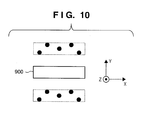
- FIGS. 9 and 10 show example arrangements of measurement points.
- three measurement points of the surface-position detecting apparatus are arranged to both the front and to the rear in the scanning direction (Y direction) of a slit light 900.
- five measurement points of the surface-position detecting apparatus are arranged to both the front and to the rear in the scanning direction (Y direction) of the slit light 900.
- Measurement points are arranged to both the front and to the rear in the slit direction so that with scanning for exposure performed in both the +Y direction and the -Y direction, the surface position of the substrate is measured immediately before exposure in either direction.
- Japanese Patent Laid-Open No. 09-045609 discloses a method for measuring the focus and tilt of scanning exposure.
- Japanese Patent Laid-Open No. 2004-071851 discloses a method for controlling and driving the focus and tilt using wafer surface information obtained in advance with a focus detecting system provided separately from an exposure apparatus.
- the miniaturization trend has been accompanied by the focal depth becoming extremely small, and thus demands for so-called focus precision, meaning the precision of matching the surface of the substrate to be exposed to an optimal image plane, have become more and more intense.
- the required control of flatness of the substrate relative to the focal depth of the exposure apparatus is ordinarily 1/10 to 1/5 of the focal depth, and is 0.04 to 0.08 ⁇ m when the focal depth is 0.4 ⁇ m.
- the surface position of the substrate is corrected based on the information of measurement points FP1, FP2, and FP3 arranged at equal intervals, information of the surface position of the substrate is not present between the measurement points. Accordingly, an offset amount ⁇ of defocusing occurs between the actual surface position of the substrate and the surface obtained from the surface position information of FP1, FP2, and FP3.
- Such a defocusing factor is referred to as focus sampling error.
- the focus sampling interval should be reduced.
- the focus sampling error can be determined based on the detection area and the sampling period of the measurement sensor, a sampling period corresponding to the residual vibration mode of the structural body of the exposure apparatus, the control frequency of the control system, or the like.
- measurement points are arranged at 1 mm intervals in the scanning direction, and light oblique incident type measurement points are arranged at 1 mm intervals in a direction perpendicular to the scanning direction.
- the surface information across the entire range of the substrate is obtained as information mapped to a grid of 1 mm intervals in the scanning direction and 1 mm intervals in the direction perpendicular to the scanning direction.
- a shot region can be configured to include one or a plurality of chip areas.
- the present invention in its first aspect provides an exposure apparatus as specified in claims 1 to 11.
- the present invention in its second aspect provides a method of manufacturing a device as specified in claim 12.
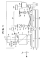
- FIG. 1 shows the overall configuration of an exposure apparatus according to an exemplary embodiment of the present invention.
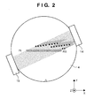
- FIG. 2 shows an example of a light beam for plane position detection in a first plane position detecting unit.
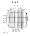
- FIG. 3 shows an example of a measurement sequence for an exposure area of a substrate.
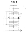
- FIG. 4 shows an example arrangement of measurement points in a surface position detecting method according to an exemplary embodiment of the present invention.
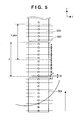
- FIG. 5 shows an example arrangement of measurement points in a surface position detecting method according to an exemplary embodiment of the present invention.
- FIG. 6 is a plan view that shows an example of selecting a sample shot for evaluating the surface state of an exposure area of a substrate.
- FIG. 7 schematically shows how the focus of a substrate surface is measured at broad intervals.
- FIG. 8 is a flowchart that shows the operation of an exposure apparatus according to an exemplary embodiment of the present invention.
- FIG. 9 shows an example arrangement of measurement points.
- FIG. 10 shows an example arrangement of measurement points.
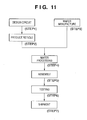
- FIG. 11 shows the overall flow of a manufacturing process for a semiconductor device.
- FIG. 12 shows the flow of a wafer process in detail.
- Embodiments of the present invention will now be described in detail with reference to the accompanying drawings.
- the embodiments reduce a disadvantage, such as local defocusing, caused by variations in the positional relationship between shot regions and measurement points among a plurality of shot regions.
- FIG. 1 shows the overall configuration of an exposure apparatus according to an exemplary embodiment of the present invention. An example is described applied to a scanning exposure apparatus.
- a scanning is driven with a reticle 2 having a pattern held by an reticle stage 3.
- the reticle 2 is output from an illumination optical system 8, and illuminated by a slit light obtained by being formed by a slit member.
- an image of the pattern of the reticle 2 is formed in the image plane of a projection optical system 1 by the slit light.
- a substrate (wafer) 4 on which a photosensitive agent (photoresist) has been applied is positioned in the image plane. Below, the substrate on which a photosensitive agent has been applied is referred to merely as the substrate.
- a plurality of shot regions are aligned on the substrate 4.
- the plurality of shot regions includes shot regions arranged along a straight line.
- Each shot region is configured including one or a plurality of chip areas.
- the exposure apparatus is configured so as to expose the plurality of shot regions on the substrate in order via the projection optical system 1.
- the substrate 4 is held by a substrate chuck 5.
- the substrate chuck 5 is mounted on an exposure stage mechanism 6.
- the exposure stage mechanism 6 is configured as an apparatus that can drive the substrate 4 in six axis-directions.
- the exposure stage mechanism 6 includes, for example, an XY stage drivable in the X and Y axis directions, a leveling stage drivable in the Z axis direction and around the X and Y axes, and a rotation stage drivable around the Z axis.
- the Z axis matches an optical axis AX of the projection optical system 1.
- the exposure stage mechanism 6 is provided on a surface plate 7.
- a first surface-position detecting unit 50 detects the surface position (or, the height position and position in the Z axis direction) and tilt of the substrate 4, and includes components 10 to 19.
- a light source 10 is configured including a white lamp, or a light emitting diode with high luminance having a plurality of distinct peak wavelengths. The light source 10 emits light beams that have approximately the same cross-sectional intensity distribution and become parallel due to the use of a collimator lens 11.
- a light beam emitted from the collimator lens 11 is incident at a plurality of measuring points (here described as 25 points) on the surface of the substrate 4, via a slit member 12, an optical system 13, and a mirror 14.
- the slit member 12 has a prism-like shape, and is formed by bonding a pair of prisms such that the sloping faces of those prisms face each other, and on the bonded face, a light shielding film constituted from chrome or the like is provided. Formed in this light shielding film are openings (for example, pin holes) corresponding to the number of measuring points.
- the optical system 13 is a double telecentric optical system.
- the angle of incidence ⁇ (angle relative to a line perpendicular to the surface of the substrate 4) of the 25 light beams on the surface of the substrate 4 is not less than 70°.
- a plurality of shot regions having the same pattern structure are aligned or defined on the surface of the substrate 4.
- the 25 light beams, after passing through the optical system 13, are incident and form an image at the measurement points of the pattern area, the measurement points being independent from each other, as shown for example in FIG. 2.
- the 25 measurement points in FIG. 2 are arranged in the X direction to cover the width (length in the direction perpendicular to the scanning direction) of the slit light on the surface of the substrate. For example, by arranging the measurement points so as to cover an area that is twice the width of the slit light on the substrate, it is possible to reduce the time needed for measurement by half.
- the optical axis of the light beam for measurement can be arranged in a direction rotated ⁇ ° (for example, 22.5°) from the X direction in the XY horizontal plane, such that the 25 measurement points are observed independently from each other on the surface of the substrate 4.
- a light beam reflected from the substrate 4 forms an image on a detection surface of a photo sensor 19 via a mirror 15, a light-receiving optical system 16, and correction optical systems 18.
- the light-receiving optical system 16 is configured as a double telecentric optical system, and inside the light-receiving optical system 16 an aperture 17 is provided.
- the aperture 17 is provided in common for the 25 measurement points, and cuts high-order diffraction light (noise light) generated by the circuit pattern present on the substrate 4.
- the optical axes of the 25 light beams become parallel to each other, images are reformed on the detection surface of the photoelectric sensor 19 by 25 individual correction lenses of the correction optical systems 18 to form 25 spots.
- the components 16 to 18 perform tilt correction such that the measurement points on the surface of the substrate 4 and the detection surface of the photoelectric sensor 19 are coupled to each other. Accordingly, changes in position of pin hole images on the detection surface occurs in response to changes in height in the optical axis direction AX of the measurement points, without allowing changes in the position of pin hole images on the detection surface due to local tilt of the measurement points.
- the photoelectric sensor 19 can be configured with 25 one-dimensional CCD line sensors, but the same effect can be obtained in a case in which the photoelectric sensor 19 is configured by providing a plurality of two-dimensional position detecting devices.
- the reticle 2 After being held by the stage of the reticle stage mechanism 3, is scanned with a constant speed in the plane perpendicular to the optical axis AX of the projection optical system 1, in the direction of arrow 3a (the Y axis direction). At this time, the reticle 2 is driven to be corrected so as to maintain a target coordinate position in the direction perpendicular to the arrow 3a (the X axis direction).
- Information of the position in the X axis and the Y axis for the stage of the reticle stage mechanism 3 is measured by irradiating a plurality of laser beams from an interference system 21 to an XY bar mirror 20 fixed to the reticle stage mechanism 3.
- An illumination optical system 8 for example, can be configured with a light source that emits pulse light such as an excimer laser, a beam shaping optical system, an optical integrator, a collimator, and a mirror.
- the illumination optical system 8 can be formed with material that effectively transmits or reflects pulse light of the far ultraviolet region.
- the beam-shaping optical system shapes the cross-sectional shape (including size) of the incident beam.
- the optical integrator allows the light distribution properties to be uniform, and illuminates the reticle 2 with uniform illumination.
- a slit-shaped illumination area is prescribed by an unshown masking blade in the illumination optical system 8, thus forming a slit light that includes the pattern information.
- An exposure station is configured with components of the illumination optical system 8, the projection optical system 1, the surface plate 7, and the like that are directly related to exposure.
- One portion of the substrate chuck 5 includes a reference surface 9.
- a separate measurement stage mechanism 22 is provided that is freely movable in six axis directions.
- the substrate 4 to be processed first, is placed on the substrate chuck mechanism 5 that is mounted on the measurement stage mechanism 22, and is held by the substrate chuck 5 with a means such as vacuum or electrostatic attraction.
- the surface position of each shot region of the substrate 4 is measured by a first surface-position detecting unit 50, using the reference surface 9 on the substrate chuck 5 as a reference.
- the results of measurement are stored in a memory 130.
- a measurement station is configured with the elements of the measurement stage mechanism 22 and the like.
- the reference surface 9 on the substrate chuck 5, in order to increase the measurement accuracy can be configured by, for example, installing a thin metal film, metal plate, or the like on the surface of the substrate chuck 5 at about the same height as the surface of the substrate 4.
- the exposure apparatus can also be configured provided with two substrate chucks 5, exchanging them between the exposure stage mechanism 6 and the measurement stage mechanism 22.
- the exposure apparatus can be configured provided with at least one (for example, two) substrate stage mechanisms, and move that substrate stage mechanism between the exposure stage and the measurement stage.
- a focusing process that matches the surface of the substrate 4 held by the substrate chuck 5 to the image plane of the projection optical system 1 is performed on the exposure stage mechanism 6.
- the focusing process while the height of the substrate 4 is measured by a second surface-position detecting unit 100 using the reference surface 9, the surface position of the substrate 4 is adjusted by the exposure stage mechanism 6.
- the focusing process can be performed using the reference surface 9 and a focusing mark 23 provided in the pattern area,of the reticle 2 or a border area thereof.
- the mark 23, for example, includes a pin hole, and light from the illumination optical system 8 having the same wavelength as the exposure light passes through the pin hole, so that with the projection optical system 1, an image is formed in the vicinity of the reference surface 9 on the substrate chuck 5.
- the projection optical system 1 With the projection optical system 1, the light reflected by the reference surface 9 again reforms an image in the vicinity of the mark 23.
- the focusing state is detected while moving the Z stage included in the exposure stage mechanism 6. The amount of light that passes through the pin hole 23 is largest when the reticle 2 and the reference surface 9 are in a completely focused state.
- the light that passes through the pin hole 23 is incident on a detector 26 via a half mirror 24 and a collector lens 25.
- the amount of light that passes through the pinhole 23 is detected by the detector 26.
- the detection results are provided to a main controller 110.
- the main controller 110 controls the exposure stage mechanism 6 via a driver 120a such that the Z stage is stopped at the position where the amount of light detected by the detector 26 is largest. Then the focusing process is finished.
- the main controller 110 controls the exposure stage mechanism 6 via a driver 120a to move the substrate chuck 5 in the XY plane, and thus exposure is performed by moving the plurality of shot regions of the substrate 4 in order to the exposure position.
- the surface of the shot region is matched to the image plane of the projection optical system 1, based on the surface position information (the position information based on the reference surface 9) of the substrate 4 already measured on the measurement stage mechanism 22 and stored in the memory 130. This is performed by the main controller 110 driving the Z stage of the exposure stage mechanism 6 via the driver 120a.
- a measurement system measures surface positions across the entire substrate 4. For example, in the order shown by way of example in FIG. 3, the substrate 4 is scanned by the measurement stage mechanism 22, and surface positions of the substrate 4 are measured in synchronism with the scanning.
- the measurement points within the shot region 300 are sequentially measured in a predetermined order.
- the substrate is moved in the X direction while quickly decelerating to move to the adjacent line.
- the surface positions of the plurality of shots lined up in the Y. direction in the manner shot region 301, shot region 302, shot region 303 are measured with constant speed.
- the substrate moves in the X direction to shift to the adjacent line while quickly decelerating, and after reaching an acceleration start point, the substrate is accelerated in the opposite direction and a plurality of shot regions in the Y direction are measured in order with constant speed.
- the procedure as described above repeats until reaching the last shot region.
- An interval P of the measurement points in the direction in which the substrate is driven can be set according to the detection area (average area) of the first surface-position detection unit 50, or the measurement scanning speed.
- the surface position can be detected as a value obtained by averaging surface positions in the detection area of the substrate.
- the detection area can be understood as an average area.
- the measurement points are arranged or defined with approximately equal spacing according to the sample pitch P.
- the first measurement point within the first shot region 401 is arranged insuring a sufficient margin M from the shot end necessary in consideration of the results of averaging surface position within the detection area with the first surface-position detection unit 50. With respect to the subsequent shot region as well, the first measurement point is arranged at a position that insures the margin M from the shot edge.
- an interval D between the last measurement point within the shot region 401 and the first measurement point within the shot region 402 is determined.
- L is the length in the scanning direction of one shot region (scanning length)
- Y pitch is the distance between shot regions.
- K INT ( L - M / P
- INT ( ) is an operator symbol wherein decimal fractions of a number are rounded off.
- a time interval T1 between the timing that one measurement point is measured and the timing that the next measurement point is measured (below, the time interval between measurement timings within a shot region) is P/S.
- the time interval T2 between the timing that the last measurement point in a shot region is measured and the timing that the first measurement point in the next shot region is measured (below, the time interval between measurement timings between shot regions) is D/S.
- the distance from the adjacent shot Y pitch is 33 [mm]
- the scanning length L is 33 [mm]
- the margin M is 0.3 [mm]
- the sample pitch P is 0.4 [mm].
- a margin of 0.3 [mm] is also insured at the position where exposure ends.
- the position of the measurement points in the next shot region depends on the position of the last measurement point in the previous shot region. Accordingly, with respect to the first measurement point of that next shot region, a sufficient margin from an edge of the shot region may not be obtained, leading to a reduction in measurement accuracy.
- the time T2 is provided, obtained by adding ⁇ T to the interval between measurement timings within a shot region. This means that in all of the shots, the margin M from an edge of the shot region to the first measurement point is insured.
- the arrangement of measurement points is the same in all of the shot regions, so that it is possible to measure the surface position with the same conditions for all of the shot regions.
- a complete shot region and an incomplete shot region may be present.
- An incomplete shot region is a shot region in which a portion protrudes from the effective area in the substrate.
- a desired position for example, an edge
- the complete shot region 502 being the first to be measured among the shot regions aligned in the scanning direction.
- the measurement timings of the measurement points of the incomplete shot region 501 and the subsequent complete shot region 503 are preferably set based on the positional relationship relative to the reference position.
- a detection error factor due to, for example, the effect of interference between light reflected by the resist surface of the substrate 4 and the light reflected by the substrate surface of the substrate 4 can be considered. That effect depends on the material of the substrate surface, which with a broad meaning is the pattern structure, and is significant enough that the effect cannot be ignored with highly reflective wiring material such as aluminum.
- an electrostatic capacitance sensor is used as a surface-position detection sensor, with a GaAs substrate used as a substrate for a high speed device or light emitting diode, it is known that there is a large measurement offset, unlike with an Si substrate.
- an offset value (correction value) is obtained to correct errors in the focus measurement value due to discrepancies in the surface state at the measurement points, i.e., errors due to the pattern structure.
- an offset value can be calculated for a plurality of sample shot regions 601 to 608 (FIG. 6) using the surface position measurement values measured while scanning the substrate.
- the measurement data at each of the measurement points stored in the memory 130 is corrected using an offset value (correction value) corresponding to the pattern structure of each measurement point.
- the sample shot arrangement in FIG. 6 is one example; the number and the arrangement of sample shot regions are not limited to those shown in this example.
- a light emitting diode (LED) is used as the light source 10
- a linear CCD sensor is used as the photo sensor 19.
- step 801 one iteration of a process is started by the main controller 110 receiving a start command.
- step 802 a substrate is placed on the chuck 5 on the measurement stage mechanism 22, and held by the chuck 5.
- step 803 the main controller 110 obtains the size (including L) of the scanning measurement area as a reference, and the time interval T1 between measurement timings within a shot region and amount of timing variation ⁇ T based on shot layout information (including Y pitch), scanning speed S, and CCD accumulation time, and stores them in the memory 130.
- step 804 under the control of the main controller 110, the entire surface of the substrate is measured while scanning at constant speed for each line with the procedure shown for example in FIG. 3.
- the surface position information (position information using the reference surface 9 as a reference) obtained as a result of measurement is stored in the memory 130.
- step s805 the main controller 110 calculates an offset value (correction value) for correcting the measurement error factor depending on the pattern structure (actual height difference within the exposure area, substrate material).
- the main controller 110 for example, as shown for example in FIG. 6, performs a calculation for the plurality of sample shot regions (601 to 608) in a diagonal line using the surface position measurement values (surface position data).
- the main controller 110 calculates an offset value (correction value) for correcting errors depending on the pattern structure.
- step 806 the main controller 110 stores the calculated offset values (correction values) in the memory 130.
- step 807 the substrate is moved onto the exposure stage mechanism 6 while being held by the substrate chuck 5.
- step 808 the Z stage of the exposure stage mechanism 6 is driven in order to focus using the reticle focusing mark 23 and the reference surface 9 on the substrate chuck.
- step 809 the main controller 110, while, using the correction values, correcting the surface position information that uses the reference surface of the substrate chuck 5 as a reference, calculates a correction-driving amount for matching the surface of the substrate 4 to the optimal-exposure image plane position. Then, the main controller 110 executes scanning exposure of the shot regions while correcting the surface position of the substrate 4 according to that correction-driving amount.
- step 810 it is judged whether or not exposure is finished for all of the shots on the substrate. If not finished, the process returns to step 809, and if exposure of all of the shots is finished, the process proceeds to step 811.
- step 811 the substrate is discharged from the exposure stage mechanism 6, and in step 812, one iteration of the exposure sequence is finished.
- the exposure apparatus of the present invention may be configured with one or a plurality of stages used both as a measurement stage and as an exposure stage.
- the exposure apparatus of the present invention may be configured provided with one or a plurality of measurement stages and a plurality of exposure stages.
- steps 801 to 811 may be executed in that order, or, in parallel with the scanning exposure from step 807 onward, the next substrate may be introduced to the measurement stage, and the process of steps 801 to 806 performed. In this case, it is possible to continuously process substrates effectively, so high efficiency exposure processing is possible.
- FIG. 11 shows the overall flow of a manufacturing process for a semiconductor device.
- circuit design circuit design of the semiconductor device is performed.
- reticle production a reticle is produced based on the designed circuit pattern.
- step 3 wafer manufacture
- step 4 wafer processing
- a pre-process in which the actual circuit is formed on the wafer with a lithography technique using the above reticle and wafer.
- step 5 (assembly) is referred to as a post-process, in which the wafer produced in step 4 is used to convert to a semiconductor chip, and includes assembly steps such as assembly (dicing, bonding) and packaging (chip enclosure).
- step 6 testing of the semiconductor device produced in step 5 is performed, such as operation testing and durability testing. A semiconductor device that has passed through these steps is completed, and is then shipped (step 7).
- FIG. 12 shows the flow of wafer processing in detail.
- step 11 oxidation
- step 12 CVD
- step 13 electrode formation
- step 14 electrodes are formed on the wafer by vapor deposition.
- step 14 ion implanting
- step 15 CMP
- step 16 resist processing
- step 17 exposure
- step 18 image development
- step 19 etching
- step 20 resist separation
Landscapes
- Physics & Mathematics (AREA)
- General Physics & Mathematics (AREA)
- Exposure And Positioning Against Photoresist Photosensitive Materials (AREA)
- Exposure Of Semiconductors, Excluding Electron Or Ion Beam Exposure (AREA)
Applications Claiming Priority (1)
| Application Number | Priority Date | Filing Date | Title |
|---|---|---|---|
| JP2006103627A JP4315455B2 (ja) | 2006-04-04 | 2006-04-04 | 露光装置及びデバイス製造方法 |
Publications (2)
| Publication Number | Publication Date |
|---|---|
| EP1843209A2 true EP1843209A2 (fr) | 2007-10-10 |
| EP1843209A3 EP1843209A3 (fr) | 2007-12-05 |
Family
ID=38239897
Family Applications (1)
| Application Number | Title | Priority Date | Filing Date |
|---|---|---|---|
| EP07105473A Withdrawn EP1843209A3 (fr) | 2006-04-04 | 2007-04-02 | Appareil d'exposition et procédé de fabrication d'un dispositif |
Country Status (5)
| Country | Link |
|---|---|
| US (2) | US7423726B2 (fr) |
| EP (1) | EP1843209A3 (fr) |
| JP (1) | JP4315455B2 (fr) |
| KR (1) | KR100875008B1 (fr) |
| TW (1) | TWI397778B (fr) |
Cited By (2)
| Publication number | Priority date | Publication date | Assignee | Title |
|---|---|---|---|---|
| CN102193327A (zh) * | 2010-03-12 | 2011-09-21 | Asml荷兰有限公司 | 光刻设备和器件制造方法 |
| CN101533228B (zh) * | 2008-03-11 | 2012-07-04 | Asml荷兰有限公司 | 测量和获取相对于衬底表面的高度数据的方法和设备 |
Families Citing this family (24)
| Publication number | Priority date | Publication date | Assignee | Title |
|---|---|---|---|---|
| JP4418699B2 (ja) * | 2004-03-24 | 2010-02-17 | キヤノン株式会社 | 露光装置 |
| JP4315455B2 (ja) * | 2006-04-04 | 2009-08-19 | キヤノン株式会社 | 露光装置及びデバイス製造方法 |
| JP2009117419A (ja) * | 2007-11-01 | 2009-05-28 | Canon Inc | 露光装置及びデバイス製造方法 |
| USD597608S1 (en) | 2008-05-19 | 2009-08-04 | Pharmedium Services, Llc | Drug administration safety label |
| JP2009295932A (ja) * | 2008-06-09 | 2009-12-17 | Canon Inc | 露光装置及びデバイス製造方法 |
| JP5335380B2 (ja) * | 2008-11-14 | 2013-11-06 | キヤノン株式会社 | 露光装置およびデバイス製造方法 |
| EP2228685B1 (fr) * | 2009-03-13 | 2018-06-27 | ASML Netherlands B.V. | Détecteur de niveau pour appareil lithographique et procédé de fabrication de dispositif |
| US8675210B2 (en) | 2009-03-13 | 2014-03-18 | Asml Netherlands B.V. | Level sensor, lithographic apparatus, and substrate surface positioning method |
| US8488107B2 (en) | 2009-03-13 | 2013-07-16 | Asml Netherlands B.V. | Lithographic apparatus and device manufacturing method involving a level sensor having multiple projection units and detection units |
| JP2011035333A (ja) * | 2009-08-05 | 2011-02-17 | Renesas Electronics Corp | 走査型露光装置、走査型露光方法、半導体装置の製造方法およびプログラム |
| US20110174086A1 (en) * | 2010-01-19 | 2011-07-21 | Divyasimha Harish | Capacitive sensor based structure and method with tilt compensation capability |
| CN102866587B (zh) * | 2011-07-08 | 2014-12-17 | 上海微电子装备有限公司 | 工件台 |
| JP6066610B2 (ja) * | 2012-07-31 | 2017-01-25 | キヤノン株式会社 | 露光方法、露光装置及びデバイス製造方法 |
| US11885738B1 (en) | 2013-01-22 | 2024-01-30 | J.A. Woollam Co., Inc. | Reflectometer, spectrophotometer, ellipsometer or polarimeter system including sample imaging system that simultaneously meet the scheimpflug condition and overcomes keystone error |
| CN104111596A (zh) * | 2013-04-16 | 2014-10-22 | 上海微电子装备有限公司 | 用于光刻设备的全局调平的装置和方法 |
| JP6299111B2 (ja) * | 2013-08-28 | 2018-03-28 | オムロン株式会社 | レーザ加工装置 |
| US11061338B2 (en) | 2014-04-17 | 2021-07-13 | Nikon Corporation | High-resolution position encoder with image sensor and encoded target pattern |
| US10812695B2 (en) * | 2015-09-14 | 2020-10-20 | Nikon Corporation | Three-dimensional positioning system using surface pattern recognition and interpolation |
| US9726987B2 (en) | 2014-04-17 | 2017-08-08 | Nikon Corporation | Positioning system using surface pattern recognition and interpolation |
| JP6748461B2 (ja) * | 2016-03-22 | 2020-09-02 | キヤノン株式会社 | インプリント装置、インプリント装置の動作方法および物品製造方法 |
| JP7287304B2 (ja) * | 2020-02-10 | 2023-06-06 | 株式会社デンソー | ワイドバンドギャップ半導体装置の製造方法 |
| CN114184621B (zh) * | 2020-09-14 | 2024-12-17 | 临颍县爬杆机器人有限公司 | 曲面零件外观缺陷检测方法及实施该方法的装置 |
| US11487210B1 (en) * | 2021-08-12 | 2022-11-01 | Taiwan Semiconductor Manufacturing Company Ltd. | Method and system of surface topography measurement for lithography |
| JP2023042984A (ja) * | 2021-09-15 | 2023-03-28 | キヤノン株式会社 | 露光装置、及び物品の製造方法 |
Family Cites Families (13)
| Publication number | Priority date | Publication date | Assignee | Title |
|---|---|---|---|---|
| JP3269343B2 (ja) * | 1995-07-26 | 2002-03-25 | キヤノン株式会社 | ベストフォーカス決定方法及びそれを用いた露光条件決定方法 |
| US6559465B1 (en) * | 1996-08-02 | 2003-05-06 | Canon Kabushiki Kaisha | Surface position detecting method having a detection timing determination |
| JP3335126B2 (ja) * | 1998-07-06 | 2002-10-15 | キヤノン株式会社 | 面位置検出装置及びそれを用いた走査型投影露光装置 |
| JP3913079B2 (ja) * | 2002-02-28 | 2007-05-09 | キヤノン株式会社 | 面位置検出装置及び方法並びに露光装置と該露光装置を用いたデバイスの製造方法 |
| KR100888472B1 (ko) * | 2002-07-06 | 2009-03-12 | 삼성전자주식회사 | 이중키를 이용한 암호화방법 및 이를 위한 무선 랜 시스템 |
| JP2004071851A (ja) | 2002-08-07 | 2004-03-04 | Canon Inc | 半導体露光方法及び露光装置 |
| JP2004266342A (ja) * | 2003-02-03 | 2004-09-24 | Sony Corp | 無線アドホック通信システム、端末、その端末における復号方法、暗号化方法及びブロードキャスト暗号鍵配布方法並びにそれらの方法を端末に実行させるためのプログラム |
| JP4652667B2 (ja) * | 2003-02-13 | 2011-03-16 | キヤノン株式会社 | 面位置計測方法及び走査型露光装置 |
| JP4315420B2 (ja) * | 2003-04-18 | 2009-08-19 | キヤノン株式会社 | 露光装置及び露光方法 |
| JP2005129674A (ja) * | 2003-10-23 | 2005-05-19 | Canon Inc | 走査露光装置およびデバイス製造方法 |
| US7061579B2 (en) * | 2003-11-13 | 2006-06-13 | Asml Netherlands B.V. | Lithographic apparatus and device manufacturing method |
| JP4418699B2 (ja) | 2004-03-24 | 2010-02-17 | キヤノン株式会社 | 露光装置 |
| JP4315455B2 (ja) | 2006-04-04 | 2009-08-19 | キヤノン株式会社 | 露光装置及びデバイス製造方法 |
-
2006
- 2006-04-04 JP JP2006103627A patent/JP4315455B2/ja not_active Expired - Fee Related
-
2007
- 2007-03-28 US US11/692,471 patent/US7423726B2/en not_active Expired - Fee Related
- 2007-04-02 EP EP07105473A patent/EP1843209A3/fr not_active Withdrawn
- 2007-04-03 KR KR1020070032613A patent/KR100875008B1/ko not_active Expired - Fee Related
- 2007-04-03 TW TW096111915A patent/TWI397778B/zh not_active IP Right Cessation
-
2008
- 2008-08-26 US US12/198,179 patent/US8107052B2/en not_active Expired - Fee Related
Cited By (4)
| Publication number | Priority date | Publication date | Assignee | Title |
|---|---|---|---|---|
| CN101533228B (zh) * | 2008-03-11 | 2012-07-04 | Asml荷兰有限公司 | 测量和获取相对于衬底表面的高度数据的方法和设备 |
| US8582082B2 (en) | 2008-03-11 | 2013-11-12 | Asml Netherlands B.V. | Method and lithographic apparatus for measuring and acquiring height data relating to a substrate surface |
| CN102193327A (zh) * | 2010-03-12 | 2011-09-21 | Asml荷兰有限公司 | 光刻设备和器件制造方法 |
| CN102193327B (zh) * | 2010-03-12 | 2013-11-06 | Asml荷兰有限公司 | 光刻设备和器件制造方法 |
Also Published As
| Publication number | Publication date |
|---|---|
| US8107052B2 (en) | 2012-01-31 |
| KR100875008B1 (ko) | 2008-12-19 |
| US7423726B2 (en) | 2008-09-09 |
| TWI397778B (zh) | 2013-06-01 |
| JP4315455B2 (ja) | 2009-08-19 |
| TW200807164A (en) | 2008-02-01 |
| EP1843209A3 (fr) | 2007-12-05 |
| KR20070099464A (ko) | 2007-10-09 |
| US20070229788A1 (en) | 2007-10-04 |
| US20080316450A1 (en) | 2008-12-25 |
| JP2007281097A (ja) | 2007-10-25 |
Similar Documents
| Publication | Publication Date | Title |
|---|---|---|
| US7423726B2 (en) | Exposure apparatus and device manufacturing method | |
| EP1413928B1 (fr) | Appareil et méthode d'exposition par balayage | |
| US6040909A (en) | Surface position detecting system and device manufacturing method using the same | |
| US7528966B2 (en) | Position detection apparatus and exposure apparatus | |
| US5610715A (en) | Displacement detecting system, an expose apparatus, and a device manufacturing method employing a scale whose displacement is detected by a selected detection head | |
| US6897949B2 (en) | Exposure apparatus and a device manufacturing method using the same | |
| JP5137879B2 (ja) | 露光装置及びデバイス製造方法 | |
| JP3335126B2 (ja) | 面位置検出装置及びそれを用いた走査型投影露光装置 | |
| US7852458B2 (en) | Exposure apparatus | |
| KR19980024115A (ko) | 투영 노광 방법 및 투영 노광 장치 | |
| JP2010258085A (ja) | 面位置検出方法 | |
| JP2009164355A (ja) | 走査露光装置およびデバイス製造方法 | |
| US20090310108A1 (en) | Exposure apparatus and method of manufacturing device | |
| JPH10209030A (ja) | 投影露光方法及び投影露光装置 | |
| JP3428825B2 (ja) | 面位置検出方法および面位置検出装置 | |
| US20100110400A1 (en) | Scanning exposure apparatus, control method therefor, and device manufacturing method | |
| JPH07219243A (ja) | 露光装置の評価方法 | |
| JPH104055A (ja) | 自動焦点合わせ装置及びそれを用いたデバイスの製造方法 | |
| JPH1140493A (ja) | 走査型露光装置およびデバイス製造方法 | |
| JP2000133563A (ja) | 露光方法及び露光装置 | |
| JPH10116781A (ja) | 面位置検出装置及びそれを用いたデバイスの製造方法 | |
| JPH1050593A (ja) | 投影露光装置及びそれを用いた半導体デバイスの製造方法 | |
| JP4026888B2 (ja) | 面位置検出装置及びそれを用いた投影露光装置 | |
| JP2005243710A (ja) | 露光装置及びその制御方法、デバイス製造方法 | |
| JPS63190334A (ja) | 投影露光方法 |
Legal Events
| Date | Code | Title | Description |
|---|---|---|---|
| PUAI | Public reference made under article 153(3) epc to a published international application that has entered the european phase |
Free format text: ORIGINAL CODE: 0009012 |
|
| AK | Designated contracting states |
Kind code of ref document: A2 Designated state(s): AT BE BG CH CY CZ DE DK EE ES FI FR GB GR HU IE IS IT LI LT LU LV MC MT NL PL PT RO SE SI SK TR |
|
| AX | Request for extension of the european patent |
Extension state: AL BA HR MK YU |
|
| PUAL | Search report despatched |
Free format text: ORIGINAL CODE: 0009013 |
|
| AK | Designated contracting states |
Kind code of ref document: A3 Designated state(s): AT BE BG CH CY CZ DE DK EE ES FI FR GB GR HU IE IS IT LI LT LU LV MC MT NL PL PT RO SE SI SK TR |
|
| AX | Request for extension of the european patent |
Extension state: AL BA HR MK YU |
|
| 17P | Request for examination filed |
Effective date: 20080605 |
|
| AKX | Designation fees paid |
Designated state(s): DE GB |
|
| STAA | Information on the status of an ep patent application or granted ep patent |
Free format text: STATUS: THE APPLICATION HAS BEEN WITHDRAWN |
|
| 18W | Application withdrawn |
Effective date: 20151209 |