EP1844566B1 - Procede de transmission optique de signaux multiplex de polarisation - Google Patents
Procede de transmission optique de signaux multiplex de polarisation Download PDFInfo
- Publication number
- EP1844566B1 EP1844566B1 EP06707832A EP06707832A EP1844566B1 EP 1844566 B1 EP1844566 B1 EP 1844566B1 EP 06707832 A EP06707832 A EP 06707832A EP 06707832 A EP06707832 A EP 06707832A EP 1844566 B1 EP1844566 B1 EP 1844566B1
- Authority
- EP
- European Patent Office
- Prior art keywords
- polarization
- signals
- signal
- wdm
- data signals
- Prior art date
- Legal status (The legal status is an assumption and is not a legal conclusion. Google has not performed a legal analysis and makes no representation as to the accuracy of the status listed.)
- Expired - Lifetime
Links
Images



Classifications
-
- H—ELECTRICITY
- H04—ELECTRIC COMMUNICATION TECHNIQUE
- H04J—MULTIPLEX COMMUNICATION
- H04J14/00—Optical multiplex systems
- H04J14/06—Polarisation multiplex systems
-
- H—ELECTRICITY
- H04—ELECTRIC COMMUNICATION TECHNIQUE
- H04J—MULTIPLEX COMMUNICATION
- H04J14/00—Optical multiplex systems
- H04J14/02—Wavelength-division multiplex systems
- H04J14/03—WDM arrangements
- H04J14/0305—WDM arrangements in end terminals
Definitions
- the invention relates to methods for transmitting polarization multiplexed signals combined to form a wavelength multiplex signal according to the preambles of claims 1 and 5.
- N modulated optical signals in the NRZ format (hereinafter also referred to as data signals) having the center wavelengths (carrier wavelengths) ⁇ 1 , ..., ⁇ N are transmitted a wavelength division multiplexer combined into a broadband optical WDM signal and transmitted in N channels.
- the WDM signal is thus a sum signal consisting of the data signals of the N signals.
- the term used is a wavelength range or frequency range used for the transmission of a data signal.
- the polarization multiplexing technique For doubling the transmission capacity in a given optical transmission channel, the polarization multiplexing technique is used.
- polarization multiplexing abbreviated to POLMUX
- two mutually orthogonally polarized data signals are transmitted at one center wavelength in an optical channel.
- the resulting signal is referred to as a polarization multiplex signal or short POLMUX signal.
- This doubles the transmission capacity of a single transmission channel.
- the polarization state of a transverse electromagnetic wave is given by the vector components of the amplitude of the electric field with respect to any but fixed rectangular coordinate system and the relative phase between the vector components of the electric field. Therefore, a change in the relative phase between the components causes a change in the polarization state of the optical wave. Consequently, in multichannel systems, non-linear effects that cause a change in the relative phase also cause a mutual change in the polarization state of the optical signals.
- the cross-phase modulation (XPM) which depends on the polarization state and the intensity of the signals involved, generally causes a change in the relative phase and thus a change in the polarization state. Their timing depends on the transmitted bit sequence of the copropagating channels.
- the resulting polarization changes as a function of time due to constantly changing bit sequences of the mutually orthogonally polarized data signals in a POLMUX signal. If the polarization states of the resultant are in agreement for two or more channels in a time interval (for example, if the same bit combination is transmitted in all the channels considered in both polarizations), XPM causes the intensity in one channel to change polarization in all other channels. Due to the constantly changing bit sequences, this leads to a noise-like change in the polarization state of each individual POLMUX signal, which equals a depolarization.
- This POLMUX specific depolarization effect which is due to the XPM, is referred to below as cross polarization modulation (XPolM).
- XPolM cross polarization modulation
- the crosstalk caused by XPolM is basically independent of the data rate and only slightly dependent on the channel spacing. Rather, XPolM depends on the overall performance of all channels and the number of channels. In WDM systems with POLMUX and a multiplicity of channels, the influence of XPolM outweighs that of XPM.
- the interference effects caused by XPolM can be reduced by lower overall performance in the individual transmission links. This can be achieved either by shortening the sections or by reducing the number of channels.
- Another way to slightly reduce XPolM is to use Raman amplifiers because it reduces the integrated power of the track. Nevertheless, the reduction in overall performance in a WDM system is true with other functional losses and reduces the influence of XPolM on the data transmission only conditionally.
- the polarization multiplexed signals are formed from two data signals each with a phase shift of 90 ° to each other.
- the invention is based on the recognition that the mutual interference between the POLMUX signals are greatest when POLMUX signals or optical data signals of the same polarization are transmitted in the channels.
- the signals transmitted in a channel form a resulting signal (resulting E-field vector), which is for example in a plane in a linear polarization and is particularly disturbing when the disturbed signal has the same plane of polarization.
- resulting POLMUX signals are transmitted which have a resulting circular polarization, then these POLMUX signals (E-field vectors) in adjacent channels rotate at different speeds because of the different wavelengths, so that a reduction from maximum to mean interference is effected.
- a first optical data signal and a second optical data signal without phase difference of their carrier signals are combined to form a polarization multiplex signal
- the carrier signal of a second optical data signal relative to the carrier signal of its first optical data signal is phase-shifted by 180 ° and combined with a first optical data signal to form a second polarization multiplex signal, so that at the same time emitting each of the optical data signals, a resulting polarization of the second polarization multiplex signal of the second channel by 90 ° from the resulting polarization of the first polarization Multiplex signal of the first channel is different.
- Disturbances due to XPolM have a particularly serious effect if, in a large number of channels, all the optical signals have the same polarization and logical 1s are transmitted.
- the resultant polarization of a channel multiplexed multiplexing signal differs by 90 ° from that of a respective adjacent polarization multiplexing signal, the above case is avoided and the interference is reduced.
- the method advantageously brings about an increase in the transmission range.
- the non-linear crosstalk is reduced anyway.
- EOP eye opening penalty
- the polarization of the POLMUX signals is advantageously controlled. This results in an optimal interference reduction.
- the polarization state of the POLMUX signals is advantageously controlled and regulated during the data transmission at at least one point in the transmission path.
- FIG. 1 shows the polarization and phase angle of two POLMUX signals in adjacent POLMUX channels K1 and K2.
- the invention will be explained with reference to two adjacent channels, corresponding results for other channels.
- Two optical data signals PS1x and PS1y modulated with the logical 1 are transmitted in the first POLMUX channel K1. Shown in a snapshot are the amplitudes of the E-field vectors. The transmission direction in a fiber is perpendicular to the plane of the drawing.
- the amplitude-modulated data signal PS1x is horizontally polarized here and the amplitude-modulated data signal PS1y is vertical polarized.
- Both signals also have a phase shift between their optical carrier signals of ⁇ 90 ° to each other (here PS1x for example -90 °, FIG. 1b ), so that a resultant POLMUX signal PMS1 has right-hand circular polarization (dashed).
- the POLMUX signals in other channels of the WDM system are also circularly polarized; However, since they have different wavelengths, the resulting fields rotate at different rotational speeds, so that there is an average interference.
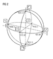
- FIG. 2 shows on the Poincaré sphere the polarization of the modulated data signals (or already their carrier signals) and the resulting polarization when transmitting two logical ones in the channel K1. If only the signal PS1x (bits 1.0 in the POLMUX channel) is transmitted, this has a horizontal polarization (in the foreground); If only the modulated data signal PS1y (0,1) is transmitted, this has a perpendicular polarization (in the background of the Poincare sphere). These two signals are orthogonal to each other and therefore influence each other only minimally. If both modulated data signals (1,1) are transmitted, the resulting POLMUX signal (1,1) has a right-hand circular polarization (south pole).
- a polarization angle ⁇ ⁇ 45 ° results in the POLMUX channel K2; on the Poincaré sphere, this corresponds to a polarization different by n / 4 (90 ° in the traditional graduation) from the individual modulated data signals PS1x and PS1y of the channel K1. If both modulated data signals (1.1, 1.1) are transmitted in both channels K1 and K2, then these are mutually orthogonal circularly polarized.
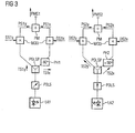
- FIG. 3 shows two principal arrangements for generating the desired signals.
- a linearly polarized signal is generated which (optionally by a polarization controller POLS) has a polarization plane of 45 °.
- This signal is transmitted through a pole splitter POLSP into a horizontally polarized carrier signal TS1x and split vertically polarized carrier signal TS1y.
- Both signals are respectively modulated with a data signal DS1x or DS1y and combined in a polarization multiplexer PM to form the POLMUX signal PMS1.
- a phase shift is achieved by a first phase shifter PH1, which here symbolically causes a phase shift of the carrier signal TS1x by -90 ° (if appropriate, PH is inserted in the signal path of the signal TS1y).
- the generation of the second POLMUX signal PMS2 takes place in a corresponding manner.
- a second laser diode LA2 generates a signal with a different wavelength, the polarization of which is optionally aligned vertically in a polarization controller POLS.
- the following polarization splitter POLSP splits the laser signal into two mutually orthogonal carrier signals TS2x and TS2y, which are each rotated by 45 ° with respect to the carrier signals of the first channel. Then, although the interference in the transmission of only one of the data signals by crosstalk never minimal but always reduced. With a high number of channels, the polarizations of the data signals can also be rotated by correspondingly smaller values, since then the interference effects average.
- the carrier signal TS2x is phase-shifted by + 90 ° by a second phase shifter PH2 compared to the other carrier signal TS2y.
- Both carrier signals are modulated with data signals DS2x or DS2y and combined in the polarization multiplexer PM to form the second POLMUX signal PMS2 which has an opposite circular polarization to the first POLMUX signal PMS1 when both carrier signals (1,1) are transmitted.
- the polarization and optionally the phase shift are kept constant by regulations.
- the method can be supplemented by additional measures that reduce the mutual influence of the POLMUX signals.
- additional measures that reduce the mutual influence of the POLMUX signals. For example, the modulated data signals during transmission by an integer Multiples of one bit length against each other to cause a decorrelation between the POLMUX signals.
- FIG. 4a represents the case of the conventional POLMUX transmission in which two modulated optical data signals PS1x and PS1y mutually orthogonally polarized are respectively transmitted in one channel (here K1 or K2) at the corresponding wavelength.
- the resulting polarization of the POLMUX signal depends on the transmitted bit pattern.
- the E-field vector of the resulting polarization of the POLMUX is Signal entered in x- or in y-direction.
- the E-field vector of the resulting polarization of the POLMUX signal lies at 45 ° to the x-direction (bit combination, 11 ').
- the polarization state of the resultant of the POLMUX signal is changed for every other channel, as in Fig. 4b is shown.
- the phase of the first modulated data signal PS2x is shifted by 180 °, which can be seen from the E-field vectors for the channel K2.
- the E-field vector points in the negative x-direction.
- the E-field vector of the resulting polarization of the POLMUX signal is less than 135 ° to the x-direction, ie the resulting one Polarization in channel K2 differs by 90 ° from the resulting polarization in channel K1.
- Which type of polarization is involved is irrelevant to the method according to the invention. It generally applies equally to linearly polarized or circularly or elliptically polarized optical signals.
- Fig. 5 the spectra of the summed from two data signals POLMUX signals for 5 channels ⁇ 1- ⁇ 5 a WDM system with increasing wavelength ⁇ are sketched (where the designation ⁇ 1- ⁇ 5 simultaneously indicates the different wavelengths of the carrier signals CW).
- each POLMUX signal PMS1 - PMS5 are based on Fig. 1 illustrates the E-field vectors of the resulting polarizations of the individual POLMUX signals for the possible bit combinations.
- Fig. 1 illustrates the E-field vectors of the resulting polarizations of the individual POLMUX signals for the possible bit combinations.
- In the case of 11 combinations of respectively two data signals PSnx and PSny (n 1, 2, 3 ..) in mutually adjacent channels, mutually orthogonal polarizations of the resulting POLMUX signals result.
- Non-linear coupling between channels of the same bit pattern is reduced due to the different polarization states of the adjacent channels. Since the bit sequences in the individual channels always change, the disturbance can not be completely eliminated due to crosstalk. Nevertheless, in a WDM system with POLMUX and the so-called "interleaved polarization" according to the invention, the system performance is always improved, since the crosstalk due to XPolM is the effect which most affects the system performance.
- AMGs polarization-preserving arrayed waveguide gratings
- FIG. 7 shows the block diagram of a transmitting side POLMUX arrangement with control device of the polarization state.
- the arrangement for generating a POLMUX signal PMSn for an arbitrary channel n will now be described.
- the first CW sub-signal / carrier signal TSnx is fed to a first modulator MOD1, where it is amplitude-modulated with a first data signal DS1.
- the amplitude modulated optical signal PSnx output at the output of the modulator MOD1 is fed to a polarization combiner PBS via a polarization actuator POLC, which adjusts the polarization by 90 °.
- the second CW sub-signal / carrier signal TSny is fed to a second modulator MOD2, where it is amplitude-modulated with a second data signal DS2.
- the output at the modulator output amplitude modulated optical data signal PSny is fed to a phase modulator PMOD, which is controlled by a control device RE. In the phase modulator PMOD a phase shift of 180 ° with respect to the optical data signal PSnx can be set.
- a phase shift of 180 ° causes a Polarization rotation of the resulting POLMUX signal of 90 °.
- the optical data signal PSny is subsequently supplied to the polarization combiner PBS, which combines it with the optical data signal PSnx to form a polarization-multiplexed signal PMSn.
- the output at the output of the polarization combiner POLMUX signal PMSn is supplied to a beam splitter ST2, the first output leads to the transmission path, while a measuring signal is passed to the control device RE via the second output.
- the polarization state of the resultant of the POLMUX signal is measured and generates a control signal KS, which is supplied to the phase modulator PMOD. In this way, the phase shift between the optical signals PSnx and PSny is set exactly.
- the specified variant of a POLMUX transmission arrangement is implemented, for example, for all even-numbered channels of the WDM system. Then, in the odd-numbered channels, the carrier phase of the modulated data signal PSnY at the phase modulator is held at 0 °.
- the POLMUX signals of the even-numbered and odd-numbered channels are combined for data transmission with polarization-maintaining waveguide gratings (English: “arrayed waveguide gratings", abbreviated AWG).
- the adjustment of the polarization and phase of the two optical signals of a POLMUX signal can optionally also take place before the data modulation.
- the carrier signal TS is split by means of a polarization splitter PBS into two mutually orthogonally polarized carrier signals TSnx and TSny of the same amplitude. These carrier signals are respectively supplied to different modulators.
- the phase adjustment takes place afterwards behind one of the modulators.
- Fig. 8 is the block diagram of a variant of a POLMUX multiplexer for the realization of the invention Process illustrated.
- the POLMUX signals PMS1, PMS3, PMS5 ... of the odd-numbered channels K1, K3, K5, ... which each consist of two mutually orthogonal data signals PSix and PSiy with odd-numbered i, are fed to the inputs of a polarization-maintaining AWG AWGU, where they to a first WDM signal WDM_PMSU.
- the channel spacing of the individual channels amounts to 100 GHz in this example.
- the output of AWGU is connected to the first input of a channel interleaver PI via a polarization maintaining fiber and a polarization actuator POLCU.
- the POLMUX signals PMS2, PMS4, PMS6 ... are fed to the inputs of a polarization-maintaining AWG AWGG, where they are combined to form a second WDM signal WDM_PMSG.
- the channel spacing of the individual channels here amounts to 100 GHz.
- the output of AWGG is connected to the second input of a channel interleaver PI via a polarization maintaining fiber and a polarization actuator POLCG.
- the WDM POLMUX signal WDM_PMS is output, which consists of N POLMUX signals with interleaved polarizations.
- the channel spacing is now 50 GHz.
- the WDM POLMUX signal WDM_PMS is split at a beam splitter ST into two sub-signals. The first sub-signal is supplied to the transmission link, the second sub-signal is a polarization-maintaining AWG AWG_N, which acts as a demultiplexer supplied.
- the polarization controllers C (Kn) of the even-numbered and odd-numbered channels are connected to the respective polarization actuators POLCG and POLCU. through the control signals CSG and CSU, the polarization state of the WDM signals WDM_PMSG and WDM_PMSU is checked and controlled.
- FIG. 9 is the block diagram of a second variant of a POLMUX transmission arrangement for implementing the method according to the invention shown.
- a first input of a beam combiner BC is supplied with a first WDM signal WDM_S1, which is composed with a channel spacing of 50 GHz from modulated optical data signals PS1y ( ⁇ 1 ), PS2y ( ⁇ 2 ),... PSNy ( ⁇ N ).
- the modulated optical data signals PS2x ( ⁇ 2 ), PS4x ( ⁇ 4 )), PS6x ( ⁇ 6 ) ... the even-numbered channels (the channel spacing is for example 100 GHz) are via phaser PS a multiplexer AWG2G, preferably from a polarization-maintaining AWG exists, supplied.
- the phase of the optical signals is shifted by 180 ° in each case.
- the polarization states of the respective signals are given in brackets as E-field vectors.
- the signal WDM_S2G combined in the multiplexer AWG2G is then fed to a signal interleaver SI.
- the modulated optical data signals PS1x ( ⁇ 1), PS3x (( ⁇ 3)), PS5x ( ⁇ 5), ... of the odd channels (the channel spacing is 100 GHz) are fed directly without any phase shift a polarization-maintaining multiplexer AWG2U where they a sub-signal WDM_S2U summarized and delivered to the output.
- the first sub-signal WDM_S2U is supplied to the signal interleaver SI.
- This may, for example, be a periodic filter with a 50 GHz period (a 50 GHz interleaver).
- the two WDM sub-signals WDM_S2U and WDM_S2G are combined to form a second WDM signal WDM_S2 with 50 GHz channel spacing.
- the second WDM signal WDMS_S2 is fed via a polarization adjuster POLS to a first input of a beam combiner BC.
- the polarization adjuster POLS causes a polarization rotation of the WDM signals WDM_S2 of 90 °.
- All individual signals of WDM_S1 have a polarization orthogonal to the signals of WDM_S2.
- the Beam combiner BC the mutually orthogonally polarized WDM signals WDM_S1 and WDM_S2 are combined and delivered to the output.
- the polarization planes are of course interchangeable.
- the second data signals PSny are fed in orthogonal to the first data signals PSnx, as can be seen in FIG Fig. 9 is shown.
- the WDM output signal WDM_PMS thus generated consists of one POLMUX signal PMS per channel, in which two modulated optical signals are mutually orthogonally polarized.
- the resulting polarization of the POLMUX signals in the even-numbered channels differs from the odd-numbered channels by 90 °. This transmission arrangement is compared to the in Fig. 8 illustrated variant with less effort to realize.
Landscapes
- Engineering & Computer Science (AREA)
- Computer Networks & Wireless Communication (AREA)
- Signal Processing (AREA)
- Optical Communication System (AREA)
Claims (11)
- Procédé de transmission optique de signaux multiplexés en polarisation (PMS1, PMS2, ...) regroupés pour former un signal multiplexé en longueur d'onde, lesquels sont formés respectivement par regroupement d'un premier signal de données optique modulé en amplitude (PS1x, PS2x, ...) et d'un deuxième signal de données optique modulé en amplitude (PS1y, PS2y, ...) et présentant une polarisation orthogonale par rapport au premier, caractérisé en ce que, dans un premier canal (K1) avec une première longueur d'onde (λ1), un premier signal multiplexé en polarisation (PMS1) est formé par deux signaux de données (PS1x, PS1y) modulés en amplitude et polarisés orthogonalement avec un déphasage de 90° entre leurs signaux porteurs (TS1x, TS1y), un premier signal multiplexé en polarisation résultant (PMS1), lequel est polarisé circulairement, étant de ce fait produit à l'émission simultanée des deux signaux de données (PS1x, PS1y ; ...), et en ce que, dans un deuxième canal (K2) avec une deuxième longueur d'onde (λ2), un deuxième signal multiplexé en polarisation (PMS2) est également formé par deux signaux de données (PS2x, PS2y) modulés en amplitude et polarisés orthogonalement avec un déphasage de 90° entre leurs signaux porteurs (TS2x, TS2y), un deuxième signal multiplexé en polarisation résultant (PMS2), lequel est polarisé circulairement en sens inverse, étant de ce fait produit à l'émission simultanée des deux signaux de données (PS2x, PS2y ; ...).
- Procédé selon la revendication 1, caractérisé en ce que les signaux de données modulés en amplitude (PS2x, PS2y) du deuxième signal multiplexé en polarisation (PMS2) sont transmis avec des polarisations ayant subi une rotation de 45° l'une par rapport à l'autre en comparaison avec les signaux de données modulés en amplitude (PS1x, PS1y, ...) du premier signal multiplexé en polarisation (PMS1).
- Procédé selon la revendication 1 ou 2, caractérisé en ce que tous les signaux de données modulés en amplitude (PS1x, PS1y; ...) de signaux impairs multiplexés en polarisation (PMS1, ...) et tous les signaux de données modulés en amplitude (PS2x, PS2y ; ...) de signaux pairs multiplexés en polarisation (PMS2) sont respectivement pareillement polarisés et sont transmis avec le même déphasage entre leurs signaux porteurs (TS1x, TS1y ; T2x, T2y ; ...).
- Procédé selon la revendication 3, caractérisé en ce que la polarisation et la phase des signaux porteurs (TS1x, TS1y ; TS2x, TS2y ; ...) sont calées et en ce que les signaux porteurs (TS1x, TS1y ; TS2x, TS2y ; ...) ainsi calés sont ensuite modulés en amplitude et regroupés pour former des signaux multiplexés en polarisation (PMS1, PMS2, ...).
- Procédé de transmission optique de signaux multiplexés en polarisation (PMS1, PMS2, ...) de longueur d'onde différente regroupés pour former un signal multiplexé en longueur d'onde, lesquels sont formés respectivement par regroupement d'un premier signal de données optique modulé en amplitude (PS1x, ...) et d'un deuxième signal de données optique modulé en amplitude (PS1y, ...) et présentant une polarisation orthogonale par rapport au premier, caractérisé en ce que, dans un premier canal (K1) avec une première longueur d'onde (A1), deux signaux de données optiques (PS1x, PS1y) modulés en amplitude et polarisés orthogonalement, sans différence de phase entre leurs signaux porteurs (TS1x, TS1y), sont regroupés pour former un signal multiplexé en polarisation (PMS1) et en ce que, dans un deuxième canal (K2) avec une deuxième longueur d'onde (λ2), deux signaux de données optiques (PS2x, PS2y) modulés en amplitude et polarisés orthogonalement, et dont les signaux porteurs sont déphasés de 180° l'un par rapport à l'autre, sont regroupés pour former un deuxième signal multiplexé en polarisation (PMS2) de sorte que, à l'émission simultanée des deux signaux de données optiques (PS1x, PS1y ; PS2x, PS2y), une polarisation résultante du deuxième signal multiplexé en polarisation (PMS2) diffère de 90° de la polarisation résultante du premier signal multiplexé en polarisation (PMS1).
- Procédé selon la revendication 5, caractérisé en ce que les signaux de données optiques (PS1x, PS1y ; ...) de canaux impairs (K1, ...) sans différence de phase entre leurs signaux porteurs (TS1x, TS1y ; ...) sont regroupés pour former des signaux multiplexés en polarisation (PMS1, ...) et en ce que, dans les canaux pairs (K2, ...), respectivement des signaux porteurs (TS2x, ...) de premiers signaux de données optiques (PS2x, ...) sont déphasés de 180° par rapport à des signaux porteurs (TS2y, ...) de deuxièmes signaux de données optiques (PS2y, ...) et sont regroupés pour former des signaux multiplexés en polarisation (PMS2, ...) des canaux impairs.
- Procédé selon la revendication 5 ou 6, caractérisé en ce que la différence de phase entre les signaux porteurs (TS1x, TS1y) des signaux de données optiques (PS1x et PS1y) d'un canal (K1) subit un réglage.
- Procédé selon la revendication 5 ou 6, caractérisé en ce que, pour obtenir le critère du réglage de phase, l'état de polarisation de la résultante d'un signal multiplexé en polarisation (PMS1, ...) est mesuré et un signal de réglage en est dérivé.
- Procédé selon la revendication 5 ou 6, caractérisé en ce que, dès avant la modulation des signaux optiques d'un signal multiplexé en polarisation (PMS1, ...), les états de polarisation et phases des signaux porteurs (TS1x, TS1y) sont calés ou réglés.
- Procédé selon la revendication 5 ou 6, caractérisé en ce que la polarisation de la résultante des signaux multiplexés en polarisation (PMS1, PMS2, ...) est contrôlée et réglée au moins une fois pendant la transmission de données.
- Procédé selon la revendication 6, caractérisé en ce que les deuxièmes signaux de données optiques (PSny) de même polarisation de tous les canaux sont regroupés pour former un premier signal WDM (WDM_S1) et envoyés sur une première entrée d'un combineur de polarisation (BC), en ce que les premiers signaux de données optiques (PSnx ; n = 1, 3, ...) de même polarisation des canaux impairs (K1, K3, ...) sont regroupés pour former un premier signal partiel WDM (WDM_S2U) et les premiers signaux de données optiques (PSnx ; n = 2, 4, ...) de même polarisation et déphasés de 180° des canaux pairs (K2, K4, ...) sont regroupés pour former un deuxième signal partiel WDM (WDM_S2G), la polarisation des deuxièmes signaux de données optiques (PS1y) étant différente de 90° par rapport à la polarisation des premiers signaux de données (PS1x) ou étant calée de manière telle que les deux signaux partiels WDM (WDM_S2U et WDM_S2G), regroupés pour former un deuxième signal WDM (WDM_S2) sont ensuite envoyés sur une deuxième entrée d'un combineur de polarisation (BC), et en ce que celui-ci délivre un signal de sortie WDM (WDM_PMS) formé par les signaux multiplexés en polarisation (PMS1, PMS2, ...) qui sont tels que la polarisation résultante entre des signaux voisins multiplexés en polarisation (PMS1, PMS2, ...) diffère de 90°.
Applications Claiming Priority (3)
| Application Number | Priority Date | Filing Date | Title |
|---|---|---|---|
| DE200510003679 DE102005003679A1 (de) | 2005-01-26 | 2005-01-26 | Verfahren zur optischen Übertragung von Polarisations-Multiplexsignalen |
| DE102005003681A DE102005003681A1 (de) | 2005-01-26 | 2005-01-26 | Verfahren zur optischen Datenübertragung mit Polarisations- und Wellenlängen-Multiplex |
| PCT/EP2006/050429 WO2006079634A1 (fr) | 2005-01-26 | 2006-01-25 | Procede de transmission optique de signaux multiplex de polarisation |
Publications (2)
| Publication Number | Publication Date |
|---|---|
| EP1844566A1 EP1844566A1 (fr) | 2007-10-17 |
| EP1844566B1 true EP1844566B1 (fr) | 2010-12-15 |
Family
ID=36088473
Family Applications (1)
| Application Number | Title | Priority Date | Filing Date |
|---|---|---|---|
| EP06707832A Expired - Lifetime EP1844566B1 (fr) | 2005-01-26 | 2006-01-25 | Procede de transmission optique de signaux multiplex de polarisation |
Country Status (8)
| Country | Link |
|---|---|
| US (1) | US7865080B2 (fr) |
| EP (1) | EP1844566B1 (fr) |
| AT (1) | ATE492080T1 (fr) |
| AU (1) | AU2006208719B2 (fr) |
| CA (1) | CA2595628C (fr) |
| DE (1) | DE502006008506D1 (fr) |
| RU (1) | RU2372730C2 (fr) |
| WO (1) | WO2006079634A1 (fr) |
Families Citing this family (73)
| Publication number | Priority date | Publication date | Assignee | Title |
|---|---|---|---|---|
| GB0718706D0 (en) | 2007-09-25 | 2007-11-07 | Creative Physics Ltd | Method and apparatus for reducing laser speckle |
| CN101505192B (zh) * | 2008-02-04 | 2011-09-21 | 华为技术有限公司 | 一种产生差分正交相移键控码光信号的方法及装置 |
| US8111996B2 (en) * | 2008-02-22 | 2012-02-07 | Infinera Corporation | Compact optical multiplexer and demultiplexer |
| ATE476801T1 (de) * | 2008-04-11 | 2010-08-15 | Alcatel Lucent | Modulationsschema mit erhöhter anzahl polarisierungszustände |
| JP5476697B2 (ja) * | 2008-09-26 | 2014-04-23 | 富士通株式会社 | 光信号送信装置 |
| US20100150555A1 (en) * | 2008-12-12 | 2010-06-17 | Zinan Wang | Automatic polarization demultiplexing for polarization division multiplexed signals |
| US9374188B2 (en) * | 2008-12-12 | 2016-06-21 | Alcatel Lucent | Optical communication using polarized transmit signal |
| US9335604B2 (en) | 2013-12-11 | 2016-05-10 | Milan Momcilo Popovich | Holographic waveguide display |
| US11726332B2 (en) | 2009-04-27 | 2023-08-15 | Digilens Inc. | Diffractive projection apparatus |
| US10795160B1 (en) | 2014-09-25 | 2020-10-06 | Rockwell Collins, Inc. | Systems for and methods of using fold gratings for dual axis expansion |
| US11300795B1 (en) | 2009-09-30 | 2022-04-12 | Digilens Inc. | Systems for and methods of using fold gratings coordinated with output couplers for dual axis expansion |
| US8233204B1 (en) | 2009-09-30 | 2012-07-31 | Rockwell Collins, Inc. | Optical displays |
| US11320571B2 (en) | 2012-11-16 | 2022-05-03 | Rockwell Collins, Inc. | Transparent waveguide display providing upper and lower fields of view with uniform light extraction |
| WO2011051437A1 (fr) * | 2009-10-29 | 2011-05-05 | Erik Agrell | Système et procédé de transmission de données |
| ES2616564T3 (es) | 2010-01-14 | 2017-06-13 | Huawei Technologies Co., Ltd. | Procedimiento y aparato para realizar de manera compatible una modulación PDM-BPSK y QPSK |
| US8659826B1 (en) | 2010-02-04 | 2014-02-25 | Rockwell Collins, Inc. | Worn display system and method without requiring real time tracking for boresight precision |
| JP5504982B2 (ja) * | 2010-03-10 | 2014-05-28 | 富士通株式会社 | 偏波多重光送信器、および、偏波多重光信号の制御方法 |
| US8862050B2 (en) * | 2010-07-30 | 2014-10-14 | Spatial Digital Systems, Inc. | Polarization diversity with portable devices via wavefront muxing techniques |
| EP2458751B1 (fr) | 2010-11-29 | 2013-11-20 | Xieon Networks S.à.r.l. | Système et procédé de communication optique |
| US9274349B2 (en) | 2011-04-07 | 2016-03-01 | Digilens Inc. | Laser despeckler based on angular diversity |
| WO2016020630A2 (fr) | 2014-08-08 | 2016-02-11 | Milan Momcilo Popovich | Illuminateur laser en guide d'ondes comprenant un dispositif de déchatoiement |
| US10670876B2 (en) | 2011-08-24 | 2020-06-02 | Digilens Inc. | Waveguide laser illuminator incorporating a despeckler |
| EP2995986B1 (fr) | 2011-08-24 | 2017-04-12 | Rockwell Collins, Inc. | Affichage de données |
| US9715067B1 (en) | 2011-09-30 | 2017-07-25 | Rockwell Collins, Inc. | Ultra-compact HUD utilizing waveguide pupil expander with surface relief gratings in high refractive index materials |
| US9366864B1 (en) | 2011-09-30 | 2016-06-14 | Rockwell Collins, Inc. | System for and method of displaying information without need for a combiner alignment detector |
| US9599813B1 (en) | 2011-09-30 | 2017-03-21 | Rockwell Collins, Inc. | Waveguide combiner system and method with less susceptibility to glare |
| US8634139B1 (en) | 2011-09-30 | 2014-01-21 | Rockwell Collins, Inc. | System for and method of catadioptric collimation in a compact head up display (HUD) |
| WO2013102759A2 (fr) | 2012-01-06 | 2013-07-11 | Milan Momcilo Popovich | Capteur d'image à contact utilisant des réseaux de bragg commutables |
| US9523852B1 (en) | 2012-03-28 | 2016-12-20 | Rockwell Collins, Inc. | Micro collimator system and method for a head up display (HUD) |
| WO2013163347A1 (fr) | 2012-04-25 | 2013-10-31 | Rockwell Collins, Inc. | Affichage grand angle holographique |
| US9933684B2 (en) | 2012-11-16 | 2018-04-03 | Rockwell Collins, Inc. | Transparent waveguide display providing upper and lower fields of view having a specific light output aperture configuration |
| US9674413B1 (en) | 2013-04-17 | 2017-06-06 | Rockwell Collins, Inc. | Vision system and method having improved performance and solar mitigation |
| US9727772B2 (en) | 2013-07-31 | 2017-08-08 | Digilens, Inc. | Method and apparatus for contact image sensing |
| US9244281B1 (en) | 2013-09-26 | 2016-01-26 | Rockwell Collins, Inc. | Display system and method using a detached combiner |
| US10732407B1 (en) | 2014-01-10 | 2020-08-04 | Rockwell Collins, Inc. | Near eye head up display system and method with fixed combiner |
| US9519089B1 (en) | 2014-01-30 | 2016-12-13 | Rockwell Collins, Inc. | High performance volume phase gratings |
| US9244280B1 (en) | 2014-03-25 | 2016-01-26 | Rockwell Collins, Inc. | Near eye display system and method for display enhancement or redundancy |
| JP6341601B2 (ja) * | 2014-04-01 | 2018-06-13 | 国立研究開発法人情報通信研究機構 | 波長多重分離器とそれを用いた波長多重器 |
| US10359736B2 (en) | 2014-08-08 | 2019-07-23 | Digilens Inc. | Method for holographic mastering and replication |
| US10241330B2 (en) | 2014-09-19 | 2019-03-26 | Digilens, Inc. | Method and apparatus for generating input images for holographic waveguide displays |
| US10088675B1 (en) | 2015-05-18 | 2018-10-02 | Rockwell Collins, Inc. | Turning light pipe for a pupil expansion system and method |
| US9715110B1 (en) | 2014-09-25 | 2017-07-25 | Rockwell Collins, Inc. | Automotive head up display (HUD) |
| EP3245444B1 (fr) | 2015-01-12 | 2021-09-08 | DigiLens Inc. | Affichage à guide d'ondes isolé de l'environnement |
| US9632226B2 (en) | 2015-02-12 | 2017-04-25 | Digilens Inc. | Waveguide grating device |
| US11366316B2 (en) | 2015-05-18 | 2022-06-21 | Rockwell Collins, Inc. | Head up display (HUD) using a light pipe |
| US10126552B2 (en) | 2015-05-18 | 2018-11-13 | Rockwell Collins, Inc. | Micro collimator system and method for a head up display (HUD) |
| US10247943B1 (en) | 2015-05-18 | 2019-04-02 | Rockwell Collins, Inc. | Head up display (HUD) using a light pipe |
| US10108010B2 (en) | 2015-06-29 | 2018-10-23 | Rockwell Collins, Inc. | System for and method of integrating head up displays and head down displays |
| CN113759555B (zh) | 2015-10-05 | 2024-09-20 | 迪吉伦斯公司 | 波导显示器 |
| US10598932B1 (en) | 2016-01-06 | 2020-03-24 | Rockwell Collins, Inc. | Head up display for integrating views of conformally mapped symbols and a fixed image source |
| WO2017162999A1 (fr) | 2016-03-24 | 2017-09-28 | Popovich Milan Momcilo | Procédé et appareil pour fournir un dispositif guide d'ondes holographique sélectif en polarisation |
| US10890707B2 (en) | 2016-04-11 | 2021-01-12 | Digilens Inc. | Holographic waveguide apparatus for structured light projection |
| EP3548939A4 (fr) | 2016-12-02 | 2020-11-25 | DigiLens Inc. | Dispositif de guide d'ondes à éclairage de sortie uniforme |
| EP3339922B1 (fr) * | 2016-12-23 | 2023-07-26 | Huawei Technologies Research & Development Belgium NV | Puce optique et procédé de couplage de la lumière |
| WO2018129398A1 (fr) | 2017-01-05 | 2018-07-12 | Digilens, Inc. | Dispositifs d'affichage tête haute vestimentaires |
| US10295824B2 (en) | 2017-01-26 | 2019-05-21 | Rockwell Collins, Inc. | Head up display with an angled light pipe |
| US10942430B2 (en) | 2017-10-16 | 2021-03-09 | Digilens Inc. | Systems and methods for multiplying the image resolution of a pixelated display |
| US20190212588A1 (en) | 2018-01-08 | 2019-07-11 | Digilens, Inc. | Systems and Methods for Manufacturing Waveguide Cells |
| US10732569B2 (en) | 2018-01-08 | 2020-08-04 | Digilens Inc. | Systems and methods for high-throughput recording of holographic gratings in waveguide cells |
| US10914950B2 (en) | 2018-01-08 | 2021-02-09 | Digilens Inc. | Waveguide architectures and related methods of manufacturing |
| KR20250004154A (ko) | 2018-01-08 | 2025-01-07 | 디지렌즈 인코포레이티드. | 광 도파관의 제조 방법 |
| WO2020023779A1 (fr) | 2018-07-25 | 2020-01-30 | Digilens Inc. | Systèmes et procédés pour fabriquer une structure optique multicouches |
| WO2020149956A1 (fr) | 2019-01-14 | 2020-07-23 | Digilens Inc. | Affichage de guide d'ondes holographique avec couche de commande de lumière |
| US20200247017A1 (en) | 2019-02-05 | 2020-08-06 | Digilens Inc. | Methods for Compensating for Optical Surface Nonuniformity |
| US20220283377A1 (en) | 2019-02-15 | 2022-09-08 | Digilens Inc. | Wide Angle Waveguide Display |
| CN113692544B (zh) | 2019-02-15 | 2025-04-22 | 迪吉伦斯公司 | 使用集成光栅提供全息波导显示的方法和装置 |
| US20200292745A1 (en) | 2019-03-12 | 2020-09-17 | Digilens Inc. | Holographic Waveguide Backlight and Related Methods of Manufacturing |
| CN114207492A (zh) | 2019-06-07 | 2022-03-18 | 迪吉伦斯公司 | 带透射光栅和反射光栅的波导及其生产方法 |
| US11681143B2 (en) | 2019-07-29 | 2023-06-20 | Digilens Inc. | Methods and apparatus for multiplying the image resolution and field-of-view of a pixelated display |
| KR102775783B1 (ko) | 2019-08-29 | 2025-02-28 | 디지렌즈 인코포레이티드. | 진공 격자 및 이의 제조 방법 |
| WO2022150841A1 (fr) | 2021-01-07 | 2022-07-14 | Digilens Inc. | Structures de réseau pour guides d'ondes de couleur |
| EP4288831A4 (fr) | 2021-03-05 | 2025-01-15 | Digilens Inc. | Structures périodiques évacuées et leurs procédés de fabrication |
| CN117806051B (zh) * | 2024-02-05 | 2024-08-30 | 电子科技大学中山学院 | 一种基于纯Pancharatnam-Berry相位调制的矢量光解复用装置 |
Family Cites Families (22)
| Publication number | Priority date | Publication date | Assignee | Title |
|---|---|---|---|---|
| US5537144A (en) * | 1990-06-11 | 1996-07-16 | Revfo, Inc. | Electro-optical display system for visually displaying polarized spatially multiplexed images of 3-D objects for use in stereoscopically viewing the same with high image quality and resolution |
| US5111322A (en) * | 1991-04-04 | 1992-05-05 | At&T Bell Laboratories | Polarization multiplexing device with solitons and method using same |
| JP2000209187A (ja) * | 1999-01-14 | 2000-07-28 | Toshiba Corp | 光通信装置 |
| US6714742B1 (en) * | 1999-05-20 | 2004-03-30 | University Of Southern California | Polarization-division multiplexing based on power encoding of different polarization channels |
| WO2000072492A1 (fr) * | 1999-05-20 | 2000-11-30 | University Of Southern California | Multiplexage par repartition de polarisations fonde sur la puissance de codage des differents canaux de polarisation |
| US7058086B2 (en) * | 1999-05-26 | 2006-06-06 | Xm Satellite Radio Inc. | Method and apparatus for concatenated convolutional encoding and interleaving |
| US6819872B2 (en) * | 1999-06-23 | 2004-11-16 | Jds Uniphase Corporation | Micro-optic delay element for use in a time division multiplexed system |
| US6850712B1 (en) * | 2000-05-31 | 2005-02-01 | Lucent Technologies Inc. | Optical fiber transmission system with polarization multiplexing to reduce stimulated brillouin scattering |
| CA2414369A1 (fr) * | 2000-07-10 | 2002-01-17 | Victor Yeeman Lo | Systeme et procede permettant d'augmenter la capacite d'un canal de reseau de communications a fibre optique |
| US7076169B2 (en) * | 2000-09-26 | 2006-07-11 | Celight, Inc. | System and method for orthogonal frequency division multiplexed optical communication |
| US6856459B1 (en) * | 2000-12-22 | 2005-02-15 | Cheetah Omni, Llc | Apparatus and method for controlling polarization of an optical signal |
| US20030090768A1 (en) | 2001-08-01 | 2003-05-15 | Xiang Liu | Long haul optical communication system |
| US7319755B2 (en) * | 2001-08-03 | 2008-01-15 | Waterstrike Incorporated | Image altering apparatus and method for providing confidential viewing of a fundamental display image |
| EP1296468A1 (fr) * | 2001-09-24 | 2003-03-26 | Alcatel | Procede de modulation et detection d'erreur de bit dans des systemes de transmission optique |
| DE10147871B4 (de) * | 2001-09-28 | 2004-01-15 | Siemens Ag | Verfahren zur Übertragung von mindestens einem ersten und zweiten Datensignal im Polarisationsmultiplex in einem optischen Übertragungssystem |
| US7280764B2 (en) * | 2002-03-01 | 2007-10-09 | Avago Technologies Fiber Ip (Singapore) Pte Ltd | Optical signal multiplexer/demultiplexer employing pseudorandom mode modulation |
| US6751002B2 (en) * | 2002-05-06 | 2004-06-15 | Intel Corporation | Method and apparatus for semiconductor-based integrated polarization modulator/compensator |
| DE10243141B4 (de) * | 2002-09-17 | 2006-05-11 | Siemens Ag | Verfahren zur Übertragung von optischen Polarisationsmultiplexsignalen |
| US7035009B1 (en) * | 2003-11-26 | 2006-04-25 | Coadna Photonics, Inc. | Apparatus and method for controlling polarization in an optical communications medium |
| US7218451B2 (en) * | 2004-02-05 | 2007-05-15 | Oplink Communications, Inc. | Integrated optical multiplexer and demultiplexer |
| US7154670B2 (en) * | 2004-03-10 | 2006-12-26 | Tyco Telecommunications (Us) Inc. | Methods and apparatus for polarization control |
| US7343100B2 (en) * | 2004-05-28 | 2008-03-11 | General Photonics Corporation | Optical communications based on optical polarization multiplexing and demultiplexing |
-
2006
- 2006-01-25 WO PCT/EP2006/050429 patent/WO2006079634A1/fr not_active Ceased
- 2006-01-25 RU RU2007132193/09A patent/RU2372730C2/ru not_active IP Right Cessation
- 2006-01-25 CA CA2595628A patent/CA2595628C/fr not_active Expired - Fee Related
- 2006-01-25 US US11/883,099 patent/US7865080B2/en not_active Expired - Fee Related
- 2006-01-25 AU AU2006208719A patent/AU2006208719B2/en not_active Ceased
- 2006-01-25 EP EP06707832A patent/EP1844566B1/fr not_active Expired - Lifetime
- 2006-01-25 DE DE502006008506T patent/DE502006008506D1/de not_active Expired - Lifetime
- 2006-01-25 AT AT06707832T patent/ATE492080T1/de not_active IP Right Cessation
Also Published As
| Publication number | Publication date |
|---|---|
| WO2006079634A1 (fr) | 2006-08-03 |
| EP1844566A1 (fr) | 2007-10-17 |
| CA2595628A1 (fr) | 2006-08-03 |
| RU2372730C2 (ru) | 2009-11-10 |
| AU2006208719A1 (en) | 2006-08-03 |
| RU2007132193A (ru) | 2009-03-10 |
| AU2006208719B2 (en) | 2009-05-28 |
| DE502006008506D1 (de) | 2011-01-27 |
| CA2595628C (fr) | 2013-04-16 |
| US20080145052A1 (en) | 2008-06-19 |
| ATE492080T1 (de) | 2011-01-15 |
| US7865080B2 (en) | 2011-01-04 |
Similar Documents
| Publication | Publication Date | Title |
|---|---|---|
| EP1844566A1 (fr) | Procede de transmission optique de signaux multiplex de polarisation | |
| DE69534362T2 (de) | Volloptischer mehrkanaliger TDM-WDM Konverter und volloptischer mehrkanaliger Zeit-Demultiplexer | |
| DE69423831T2 (de) | Polarisationsunabhängiger optischer Vier-Photon-Mischer mit orthogonal polarisierten Pumpsignalen | |
| DE69424311T2 (de) | Querverbindungssystem für ein optisches netzwerk | |
| DE69605542T2 (de) | Optische mehrkanalanordnung | |
| DE102022209861A1 (de) | Systeme, vorrichtungen und verfahren zur rückgewinnung der dualen polarisation | |
| EP1097531A1 (fr) | Procede de compensation de dispersion en mode polarisation et compensateur de dispersion en mode polarisation | |
| DE69522711T2 (de) | Knoten in optischem tdm-netz | |
| WO2010142285A2 (fr) | Procédé et dispositif de transmission d'informations optiques entre une station d'émission et une station de réception par l'intermédiaire d'un guide d'onde optique multimodal | |
| DE69533536T2 (de) | Polarisationsmodulation in Wellenlängen-Multiplex Übertragungssystemen | |
| DE10310015B4 (de) | Optoelektrischer Phasenregelkreis zur Rückgewinnung des Taktsignals in einem digitalen optischen Übertragungssystem | |
| WO2003096584A1 (fr) | Procede et dispositif pour limiter la degradation de signal d'un signal multiplexe en polarisation optique | |
| DE60034099T2 (de) | Vorrichtung zur Kompensation von Polarisationsmodendispersion in einem optischen Übertragungssystem | |
| EP1797654B1 (fr) | Procede et dispositif de transmission optique de signaux de donnees par modulation de phase differentielle dans un procede de multiplexage de polarisation | |
| AT505320B1 (de) | Verfahren und vorrichtung zum nachregeln einer polarisationsdrift | |
| DE102005003681A1 (de) | Verfahren zur optischen Datenübertragung mit Polarisations- und Wellenlängen-Multiplex | |
| DE60200221T2 (de) | Optischer Sender, System und Verfahren zur Übertragung von Signalen mit hohen Datenraten | |
| DE60205271T2 (de) | Übertragung von optischen signalen | |
| WO2001019009A1 (fr) | Dispositif et procede de transmission optique d'informations | |
| DE69533772T2 (de) | Dynamisch kontrollierte Polarisationsmodulation in Wellenlängenmultiplex-Übertragungssystemen | |
| DE60208873T2 (de) | Empfänger zum Empfang von OTDM/PDM optischen Signalen | |
| DE102005003679A1 (de) | Verfahren zur optischen Übertragung von Polarisations-Multiplexsignalen | |
| WO2005081572A2 (fr) | Connecteur croise pour signaux optiques utilisant une technique de multiplexage temporel | |
| DE10137874B4 (de) | Add-Drop Multiplexer für OTDM-Signale | |
| WO2001084748A1 (fr) | Recepteur pour transmission optique d'informations |
Legal Events
| Date | Code | Title | Description |
|---|---|---|---|
| PUAI | Public reference made under article 153(3) epc to a published international application that has entered the european phase |
Free format text: ORIGINAL CODE: 0009012 |
|
| 17P | Request for examination filed |
Effective date: 20070827 |
|
| AK | Designated contracting states |
Kind code of ref document: A1 Designated state(s): AT BE BG CH CY CZ DE DK EE ES FI FR GB GR HU IE IS IT LI LT LU LV MC NL PL PT RO SE SI SK TR |
|
| RAP3 | Party data changed (applicant data changed or rights of an application transferred) |
Owner name: NOKIA SIEMENS NETWORKS S.P.A. |
|
| RAP3 | Party data changed (applicant data changed or rights of an application transferred) |
Owner name: NOKIA SIEMENS NETWORKS GMBH & CO. KG |
|
| DAX | Request for extension of the european patent (deleted) | ||
| GRAP | Despatch of communication of intention to grant a patent |
Free format text: ORIGINAL CODE: EPIDOSNIGR1 |
|
| GRAS | Grant fee paid |
Free format text: ORIGINAL CODE: EPIDOSNIGR3 |
|
| GRAA | (expected) grant |
Free format text: ORIGINAL CODE: 0009210 |
|
| AK | Designated contracting states |
Kind code of ref document: B1 Designated state(s): AT BE BG CH CY CZ DE DK EE ES FI FR GB GR HU IE IS IT LI LT LU LV MC NL PL PT RO SE SI SK TR |
|
| REG | Reference to a national code |
Ref country code: GB Ref legal event code: FG4D Free format text: NOT ENGLISH Ref country code: CH Ref legal event code: EP |
|
| REG | Reference to a national code |
Ref country code: IE Ref legal event code: FG4D |
|
| REF | Corresponds to: |
Ref document number: 502006008506 Country of ref document: DE Date of ref document: 20110127 Kind code of ref document: P |
|
| REG | Reference to a national code |
Ref country code: NL Ref legal event code: VDEP Effective date: 20101215 |
|
| PG25 | Lapsed in a contracting state [announced via postgrant information from national office to epo] |
Ref country code: LT Free format text: LAPSE BECAUSE OF FAILURE TO SUBMIT A TRANSLATION OF THE DESCRIPTION OR TO PAY THE FEE WITHIN THE PRESCRIBED TIME-LIMIT Effective date: 20101215 |
|
| LTIE | Lt: invalidation of european patent or patent extension |
Effective date: 20101215 |
|
| PG25 | Lapsed in a contracting state [announced via postgrant information from national office to epo] |
Ref country code: NL Free format text: LAPSE BECAUSE OF FAILURE TO SUBMIT A TRANSLATION OF THE DESCRIPTION OR TO PAY THE FEE WITHIN THE PRESCRIBED TIME-LIMIT Effective date: 20101215 Ref country code: SE Free format text: LAPSE BECAUSE OF FAILURE TO SUBMIT A TRANSLATION OF THE DESCRIPTION OR TO PAY THE FEE WITHIN THE PRESCRIBED TIME-LIMIT Effective date: 20101215 Ref country code: CY Free format text: LAPSE BECAUSE OF FAILURE TO SUBMIT A TRANSLATION OF THE DESCRIPTION OR TO PAY THE FEE WITHIN THE PRESCRIBED TIME-LIMIT Effective date: 20101215 Ref country code: LV Free format text: LAPSE BECAUSE OF FAILURE TO SUBMIT A TRANSLATION OF THE DESCRIPTION OR TO PAY THE FEE WITHIN THE PRESCRIBED TIME-LIMIT Effective date: 20101215 Ref country code: BG Free format text: LAPSE BECAUSE OF FAILURE TO SUBMIT A TRANSLATION OF THE DESCRIPTION OR TO PAY THE FEE WITHIN THE PRESCRIBED TIME-LIMIT Effective date: 20110315 Ref country code: SI Free format text: LAPSE BECAUSE OF FAILURE TO SUBMIT A TRANSLATION OF THE DESCRIPTION OR TO PAY THE FEE WITHIN THE PRESCRIBED TIME-LIMIT Effective date: 20101215 Ref country code: FI Free format text: LAPSE BECAUSE OF FAILURE TO SUBMIT A TRANSLATION OF THE DESCRIPTION OR TO PAY THE FEE WITHIN THE PRESCRIBED TIME-LIMIT Effective date: 20101215 |
|
| REG | Reference to a national code |
Ref country code: IE Ref legal event code: FD4D |
|
| PG25 | Lapsed in a contracting state [announced via postgrant information from national office to epo] |
Ref country code: EE Free format text: LAPSE BECAUSE OF FAILURE TO SUBMIT A TRANSLATION OF THE DESCRIPTION OR TO PAY THE FEE WITHIN THE PRESCRIBED TIME-LIMIT Effective date: 20101215 Ref country code: ES Free format text: LAPSE BECAUSE OF FAILURE TO SUBMIT A TRANSLATION OF THE DESCRIPTION OR TO PAY THE FEE WITHIN THE PRESCRIBED TIME-LIMIT Effective date: 20110326 Ref country code: PT Free format text: LAPSE BECAUSE OF FAILURE TO SUBMIT A TRANSLATION OF THE DESCRIPTION OR TO PAY THE FEE WITHIN THE PRESCRIBED TIME-LIMIT Effective date: 20110415 Ref country code: CZ Free format text: LAPSE BECAUSE OF FAILURE TO SUBMIT A TRANSLATION OF THE DESCRIPTION OR TO PAY THE FEE WITHIN THE PRESCRIBED TIME-LIMIT Effective date: 20101215 Ref country code: GR Free format text: LAPSE BECAUSE OF FAILURE TO SUBMIT A TRANSLATION OF THE DESCRIPTION OR TO PAY THE FEE WITHIN THE PRESCRIBED TIME-LIMIT Effective date: 20110316 Ref country code: IE Free format text: LAPSE BECAUSE OF FAILURE TO SUBMIT A TRANSLATION OF THE DESCRIPTION OR TO PAY THE FEE WITHIN THE PRESCRIBED TIME-LIMIT Effective date: 20101215 Ref country code: IS Free format text: LAPSE BECAUSE OF FAILURE TO SUBMIT A TRANSLATION OF THE DESCRIPTION OR TO PAY THE FEE WITHIN THE PRESCRIBED TIME-LIMIT Effective date: 20110415 |
|
| BERE | Be: lapsed |
Owner name: NOKIA SIEMENS NETWORKS G.M.B.H. & CO. KG Effective date: 20110131 |
|
| PG25 | Lapsed in a contracting state [announced via postgrant information from national office to epo] |
Ref country code: PL Free format text: LAPSE BECAUSE OF FAILURE TO SUBMIT A TRANSLATION OF THE DESCRIPTION OR TO PAY THE FEE WITHIN THE PRESCRIBED TIME-LIMIT Effective date: 20101215 Ref country code: SK Free format text: LAPSE BECAUSE OF FAILURE TO SUBMIT A TRANSLATION OF THE DESCRIPTION OR TO PAY THE FEE WITHIN THE PRESCRIBED TIME-LIMIT Effective date: 20101215 Ref country code: RO Free format text: LAPSE BECAUSE OF FAILURE TO SUBMIT A TRANSLATION OF THE DESCRIPTION OR TO PAY THE FEE WITHIN THE PRESCRIBED TIME-LIMIT Effective date: 20101215 Ref country code: MC Free format text: LAPSE BECAUSE OF NON-PAYMENT OF DUE FEES Effective date: 20110131 |
|
| REG | Reference to a national code |
Ref country code: CH Ref legal event code: PL |
|
| PLBE | No opposition filed within time limit |
Free format text: ORIGINAL CODE: 0009261 |
|
| STAA | Information on the status of an ep patent application or granted ep patent |
Free format text: STATUS: NO OPPOSITION FILED WITHIN TIME LIMIT |
|
| PG25 | Lapsed in a contracting state [announced via postgrant information from national office to epo] |
Ref country code: DK Free format text: LAPSE BECAUSE OF FAILURE TO SUBMIT A TRANSLATION OF THE DESCRIPTION OR TO PAY THE FEE WITHIN THE PRESCRIBED TIME-LIMIT Effective date: 20101215 Ref country code: LI Free format text: LAPSE BECAUSE OF NON-PAYMENT OF DUE FEES Effective date: 20110131 Ref country code: CH Free format text: LAPSE BECAUSE OF NON-PAYMENT OF DUE FEES Effective date: 20110131 |
|
| 26N | No opposition filed |
Effective date: 20110916 |
|
| PG25 | Lapsed in a contracting state [announced via postgrant information from national office to epo] |
Ref country code: BE Free format text: LAPSE BECAUSE OF NON-PAYMENT OF DUE FEES Effective date: 20110131 |
|
| PG25 | Lapsed in a contracting state [announced via postgrant information from national office to epo] |
Ref country code: IT Free format text: LAPSE BECAUSE OF FAILURE TO SUBMIT A TRANSLATION OF THE DESCRIPTION OR TO PAY THE FEE WITHIN THE PRESCRIBED TIME-LIMIT Effective date: 20101215 |
|
| REG | Reference to a national code |
Ref country code: DE Ref legal event code: R097 Ref document number: 502006008506 Country of ref document: DE Effective date: 20110916 |
|
| REG | Reference to a national code |
Ref country code: AT Ref legal event code: MM01 Ref document number: 492080 Country of ref document: AT Kind code of ref document: T Effective date: 20110125 |
|
| PG25 | Lapsed in a contracting state [announced via postgrant information from national office to epo] |
Ref country code: AT Free format text: LAPSE BECAUSE OF NON-PAYMENT OF DUE FEES Effective date: 20110125 |
|
| PG25 | Lapsed in a contracting state [announced via postgrant information from national office to epo] |
Ref country code: LU Free format text: LAPSE BECAUSE OF NON-PAYMENT OF DUE FEES Effective date: 20110125 |
|
| PG25 | Lapsed in a contracting state [announced via postgrant information from national office to epo] |
Ref country code: TR Free format text: LAPSE BECAUSE OF FAILURE TO SUBMIT A TRANSLATION OF THE DESCRIPTION OR TO PAY THE FEE WITHIN THE PRESCRIBED TIME-LIMIT Effective date: 20101215 |
|
| PG25 | Lapsed in a contracting state [announced via postgrant information from national office to epo] |
Ref country code: HU Free format text: LAPSE BECAUSE OF FAILURE TO SUBMIT A TRANSLATION OF THE DESCRIPTION OR TO PAY THE FEE WITHIN THE PRESCRIBED TIME-LIMIT Effective date: 20101215 |
|
| REG | Reference to a national code |
Ref country code: DE Ref legal event code: R082 Ref document number: 502006008506 Country of ref document: DE Representative=s name: BOEHMERT & BOEHMERT, DE |
|
| REG | Reference to a national code |
Ref country code: DE Ref legal event code: R082 Ref document number: 502006008506 Country of ref document: DE Representative=s name: BOEHMERT & BOEHMERT ANWALTSPARTNERSCHAFT MBB -, DE Effective date: 20131106 Ref country code: DE Ref legal event code: R082 Ref document number: 502006008506 Country of ref document: DE Representative=s name: BOEHMERT & BOEHMERT, DE Effective date: 20131106 Ref country code: DE Ref legal event code: R081 Ref document number: 502006008506 Country of ref document: DE Owner name: XIEON NETWORKS S.A.R.L., LU Free format text: FORMER OWNER: NOKIA SIEMENS NETWORKS GMBH & CO. KG, 81541 MUENCHEN, DE Effective date: 20131106 |
|
| REG | Reference to a national code |
Ref country code: GB Ref legal event code: 732E Free format text: REGISTERED BETWEEN 20131212 AND 20131218 |
|
| REG | Reference to a national code |
Ref country code: GB Ref legal event code: 732E Free format text: REGISTERED BETWEEN 20140130 AND 20140205 |
|
| PGFP | Annual fee paid to national office [announced via postgrant information from national office to epo] |
Ref country code: DE Payment date: 20140130 Year of fee payment: 9 |
|
| REG | Reference to a national code |
Ref country code: FR Ref legal event code: TP Owner name: XIEON NETWORKS S.A.R.L., LU Effective date: 20140408 Ref country code: FR Ref legal event code: GC Effective date: 20140408 |
|
| PGFP | Annual fee paid to national office [announced via postgrant information from national office to epo] |
Ref country code: FR Payment date: 20140130 Year of fee payment: 9 |
|
| PGFP | Annual fee paid to national office [announced via postgrant information from national office to epo] |
Ref country code: GB Payment date: 20140130 Year of fee payment: 9 |
|
| REG | Reference to a national code |
Ref country code: DE Ref legal event code: R119 Ref document number: 502006008506 Country of ref document: DE |
|
| GBPC | Gb: european patent ceased through non-payment of renewal fee |
Effective date: 20150125 |
|
| PG25 | Lapsed in a contracting state [announced via postgrant information from national office to epo] |
Ref country code: DE Free format text: LAPSE BECAUSE OF NON-PAYMENT OF DUE FEES Effective date: 20150801 Ref country code: GB Free format text: LAPSE BECAUSE OF NON-PAYMENT OF DUE FEES Effective date: 20150125 |
|
| REG | Reference to a national code |
Ref country code: FR Ref legal event code: ST Effective date: 20150930 |
|
| PG25 | Lapsed in a contracting state [announced via postgrant information from national office to epo] |
Ref country code: FR Free format text: LAPSE BECAUSE OF NON-PAYMENT OF DUE FEES Effective date: 20150202 |