EP1860703A1 - Lichtsensitives Halbleiterbauelement mit Ladungsträgervervielfachung - Google Patents
Lichtsensitives Halbleiterbauelement mit Ladungsträgervervielfachung Download PDFInfo
- Publication number
- EP1860703A1 EP1860703A1 EP07108665A EP07108665A EP1860703A1 EP 1860703 A1 EP1860703 A1 EP 1860703A1 EP 07108665 A EP07108665 A EP 07108665A EP 07108665 A EP07108665 A EP 07108665A EP 1860703 A1 EP1860703 A1 EP 1860703A1
- Authority
- EP
- European Patent Office
- Prior art keywords
- layer
- receiving device
- conduction
- semiconductor light
- multiplication
- Prior art date
- Legal status (The legal status is an assumption and is not a legal conclusion. Google has not performed a legal analysis and makes no representation as to the accuracy of the status listed.)
- Withdrawn
Links
- 239000004065 semiconductor Substances 0.000 title claims abstract description 67
- 230000031700 light absorption Effects 0.000 claims abstract description 85
- 238000009792 diffusion process Methods 0.000 claims abstract description 28
- 239000012535 impurity Substances 0.000 claims abstract description 19
- 230000005684 electric field Effects 0.000 claims description 65
- 239000000872 buffer Substances 0.000 claims description 25
- 230000002093 peripheral effect Effects 0.000 claims description 3
- 230000014509 gene expression Effects 0.000 description 24
- 230000015556 catabolic process Effects 0.000 description 23
- 229910000530 Gallium indium arsenide Inorganic materials 0.000 description 12
- 238000004891 communication Methods 0.000 description 10
- 239000000758 substrate Substances 0.000 description 6
- XUIMIQQOPSSXEZ-UHFFFAOYSA-N Silicon Chemical compound [Si] XUIMIQQOPSSXEZ-UHFFFAOYSA-N 0.000 description 5
- 239000000969 carrier Substances 0.000 description 5
- 239000013307 optical fiber Substances 0.000 description 5
- 229910052710 silicon Inorganic materials 0.000 description 5
- 239000010703 silicon Substances 0.000 description 5
- 230000003287 optical effect Effects 0.000 description 4
- 230000004044 response Effects 0.000 description 4
- 230000035945 sensitivity Effects 0.000 description 4
- 238000006731 degradation reaction Methods 0.000 description 3
- 239000002019 doping agent Substances 0.000 description 3
- 238000004519 manufacturing process Methods 0.000 description 3
- 238000000034 method Methods 0.000 description 3
- 239000000126 substance Substances 0.000 description 3
- 229910052581 Si3N4 Inorganic materials 0.000 description 2
- 238000005094 computer simulation Methods 0.000 description 2
- 230000000694 effects Effects 0.000 description 2
- 239000000463 material Substances 0.000 description 2
- 238000002488 metal-organic chemical vapour deposition Methods 0.000 description 2
- HQVNEWCFYHHQES-UHFFFAOYSA-N silicon nitride Chemical compound N12[Si]34N5[Si]62N3[Si]51N64 HQVNEWCFYHHQES-UHFFFAOYSA-N 0.000 description 2
- 229910000980 Aluminium gallium arsenide Inorganic materials 0.000 description 1
- 229910001218 Gallium arsenide Inorganic materials 0.000 description 1
- 206010034972 Photosensitivity reaction Diseases 0.000 description 1
- 230000004888 barrier function Effects 0.000 description 1
- 229910052793 cadmium Inorganic materials 0.000 description 1
- 230000008859 change Effects 0.000 description 1
- 230000001276 controlling effect Effects 0.000 description 1
- 239000013078 crystal Substances 0.000 description 1
- 230000007423 decrease Effects 0.000 description 1
- 230000003247 decreasing effect Effects 0.000 description 1
- 238000005530 etching Methods 0.000 description 1
- 230000001747 exhibiting effect Effects 0.000 description 1
- 125000005842 heteroatom Chemical group 0.000 description 1
- 238000005468 ion implantation Methods 0.000 description 1
- 239000002184 metal Substances 0.000 description 1
- 229910052751 metal Inorganic materials 0.000 description 1
- 230000004048 modification Effects 0.000 description 1
- 238000012986 modification Methods 0.000 description 1
- 230000036211 photosensitivity Effects 0.000 description 1
- 230000008569 process Effects 0.000 description 1
- 230000001105 regulatory effect Effects 0.000 description 1
- 238000007669 thermal treatment Methods 0.000 description 1
- 229910052725 zinc Inorganic materials 0.000 description 1
Images







Classifications
-
- H—ELECTRICITY
- H10—SEMICONDUCTOR DEVICES; ELECTRIC SOLID-STATE DEVICES NOT OTHERWISE PROVIDED FOR
- H10F—INORGANIC SEMICONDUCTOR DEVICES SENSITIVE TO INFRARED RADIATION, LIGHT, ELECTROMAGNETIC RADIATION OF SHORTER WAVELENGTH OR CORPUSCULAR RADIATION
- H10F30/00—Individual radiation-sensitive semiconductor devices in which radiation controls the flow of current through the devices, e.g. photodetectors
- H10F30/20—Individual radiation-sensitive semiconductor devices in which radiation controls the flow of current through the devices, e.g. photodetectors the devices having potential barriers, e.g. phototransistors
- H10F30/21—Individual radiation-sensitive semiconductor devices in which radiation controls the flow of current through the devices, e.g. photodetectors the devices having potential barriers, e.g. phototransistors the devices being sensitive to infrared, visible or ultraviolet radiation
- H10F30/22—Individual radiation-sensitive semiconductor devices in which radiation controls the flow of current through the devices, e.g. photodetectors the devices having potential barriers, e.g. phototransistors the devices being sensitive to infrared, visible or ultraviolet radiation the devices having only one potential barrier, e.g. photodiodes
- H10F30/225—Individual radiation-sensitive semiconductor devices in which radiation controls the flow of current through the devices, e.g. photodetectors the devices having potential barriers, e.g. phototransistors the devices being sensitive to infrared, visible or ultraviolet radiation the devices having only one potential barrier, e.g. photodiodes the potential barrier working in avalanche mode, e.g. avalanche photodiodes
- H10F30/2255—Individual radiation-sensitive semiconductor devices in which radiation controls the flow of current through the devices, e.g. photodetectors the devices having potential barriers, e.g. phototransistors the devices being sensitive to infrared, visible or ultraviolet radiation the devices having only one potential barrier, e.g. photodiodes the potential barrier working in avalanche mode, e.g. avalanche photodiodes in which the active layers form heterostructures, e.g. SAM structures
-
- H—ELECTRICITY
- H10—SEMICONDUCTOR DEVICES; ELECTRIC SOLID-STATE DEVICES NOT OTHERWISE PROVIDED FOR
- H10F—INORGANIC SEMICONDUCTOR DEVICES SENSITIVE TO INFRARED RADIATION, LIGHT, ELECTROMAGNETIC RADIATION OF SHORTER WAVELENGTH OR CORPUSCULAR RADIATION
- H10F77/00—Constructional details of devices covered by this subclass
- H10F77/10—Semiconductor bodies
- H10F77/12—Active materials
- H10F77/124—Active materials comprising only Group III-V materials, e.g. GaAs
-
- H—ELECTRICITY
- H10—SEMICONDUCTOR DEVICES; ELECTRIC SOLID-STATE DEVICES NOT OTHERWISE PROVIDED FOR
- H10F—INORGANIC SEMICONDUCTOR DEVICES SENSITIVE TO INFRARED RADIATION, LIGHT, ELECTROMAGNETIC RADIATION OF SHORTER WAVELENGTH OR CORPUSCULAR RADIATION
- H10F77/00—Constructional details of devices covered by this subclass
- H10F77/10—Semiconductor bodies
- H10F77/14—Shape of semiconductor bodies; Shapes, relative sizes or dispositions of semiconductor regions within semiconductor bodies
- H10F77/148—Shapes of potential barriers
-
- Y—GENERAL TAGGING OF NEW TECHNOLOGICAL DEVELOPMENTS; GENERAL TAGGING OF CROSS-SECTIONAL TECHNOLOGIES SPANNING OVER SEVERAL SECTIONS OF THE IPC; TECHNICAL SUBJECTS COVERED BY FORMER USPC CROSS-REFERENCE ART COLLECTIONS [XRACs] AND DIGESTS
- Y02—TECHNOLOGIES OR APPLICATIONS FOR MITIGATION OR ADAPTATION AGAINST CLIMATE CHANGE
- Y02E—REDUCTION OF GREENHOUSE GAS [GHG] EMISSIONS, RELATED TO ENERGY GENERATION, TRANSMISSION OR DISTRIBUTION
- Y02E10/00—Energy generation through renewable energy sources
- Y02E10/50—Photovoltaic [PV] energy
- Y02E10/544—Solar cells from Group III-V materials
Definitions
- This invention generally relates to semiconductor light-receiving devices suitably used for optical fiber communication systems, and more particularly, to a photodiode having a multiplication function due to impact ionization.
- Fig. 1 is a schematic cross-sectional view of a conventional InP/InGaAs avalanche photodiode (APD) used for optical communications (see Japanese Patent Application Publication No. 5-21830 ).
- APD avalanche photodiode
- FIG. 1 there is provided an n + -type InP substrate 10, on which layers 12, 14, 22, 32 and 40 are provided in this order.
- the layer 12 is an n + -type InP conduction layer
- the layer 14 is an undoped InGaAs light absorption layer 14.
- the layer 22 is an InGaAsP buffer layer
- the layer 32 is an n + -type InP electric field drop layer.
- the layer 40 is an InP window layer.
- An antireflection layer 52 is provided in a light-receiving region 58 on the surface of the InP window layer 40.
- a p-type contact electrode 50 is provided around the light-receiving region 58.
- a protection film 54 is formed around the p-type contact electrode 50.
- a p + -type conduction region 42 is formed within the InP window layer 40 in the light-receiving region 58.
- a p - -type guard ring region 44 which is deeper than the p + -type conduction region 42, is provided around the p + -type conduction region 42.
- An n-type contact electrode 60 is provided on the backside of the substrate 10.
- An undoped layer 24 is formed within the window layer 40 between the p + -type conduction region 42 and the electric field drop layer 32.
- the window layer 40 has a band gap greater than that of the light absorption layer 14.
- light incident to the light-receiving region 58 passes through the window layer 40 and is then absorbed by the light absorption layer 14.
- Holes among electron-hole pairs produced in the light absorption layer 14 are injected into a multiplication layer 20, which is interposed between the light absorption layer 14 and the p + -type conduction region 42 due to the reverse biasing applied at the pn junction.
- the multiplication layer 20 functions to multiply holes (carriers) injected from the light absorption layer 14.
- the band gap of the buffer layer 22 changes continuously.
- the electric field drop layer 32 is doped to have the n + -type, and drops the electric field in the multiplication layer 20 and the light absorption layer 14.
- the holes are accelerated in the electric field drop layer 32, and carrier multiplication takes place in the upper portion of the electric field drop layer 32 and the undoped layer 24, so that the electron-hole pairs can be multiplied.
- the holes thus multiplied reach the p + -type conduction region 42.
- a multiplication factor M is defined as a ratio of the number of carriers taken out of the multiplying region to the number of carriers injected to the multiplying region.
- the APD has a planar structure in which the p + -type conduction region 42 is formed by selective diffusion.
- an edge breakdown takes places in the periphery of the p + -type conduction region 42 prior to a breakdown that takes places at the center of the p + -type conduction region 42.
- the edge breakdown is more likely to occur as the curvature radius in the periphery of the p + -type conduction region 42 decreases or the slope of impurity concentration increases.
- the edge breakdown merely results in the flow of current even when the reverse voltage is increased, and hardly increases the reverse voltage at the pn junction of the light-receiving region 58 in the center portion of the p + -type conduction region 42.
- the device is no longer capable of exhibiting the function as APD.
- the guard ring 44 is provided around the p + -type conduction region 42 in order to make the breakdown voltage in the vicinity of the p + -type conduction region 42 higher than the breakdown voltage in the flat portion (light-receiving region 58) in the center of the p + -type conduction region 42.
- the multiplication factor M of the APD for optical communications shown in Fig. 1 is generally up to about 15 in practical use.
- the multiplication factor M is increased, the frequency response is restricted and excess noise is increased because of the product of the multiplication factor and the bandwidth (MB product).
- the operating voltage is needed to be as high as at least 50 V for a high multiplication factor.
- the multiplication factor (output current) varies greatly as the light incident power varies at a high multiplication factor.
- the voltage is regulated in practical use so that the multiplication factor (output current) can be kept constant.
- the APD is used along with a high voltage power source and a bias voltage control device (driver).
- a PIN photodiode (PIN-PD) that does not have carrier multiplication can operate at a low voltage equal to or lower than 20 V, and does not change the photosensitivity (output current) to variations in incident light.
- the PIN-PD may be operated at a contact voltage with a simple drive circuit without any voltage control.
- the PIN-PD does not need the high voltage power source and the bias voltage control device (driver) necessary for the APD operation.
- the structure shown in fig. 1 employs the guard ring 44 provided around the p + -type conduction region 42 in order to avoid the edge breakdown.
- the guard ring 44 is defined by ordinary diffusion or ion implantation and a subsequent thermal treatment at a significantly high temperature.
- the guard ring 44 thus defined functions to reduce the slope of impurity concentration at the pn junction.
- the guard ring 44 directly affects the device reliability.
- the guard ring 44 defined through a complicated production process including a huge number of steps.
- the APD having the structure shown in Fig. 1 is much more expensive than the PIN-PD. Therefore, the expensive APD is used for backbone systems in the optical communications system and PID photodiode is used for less expensive subscriber systems.
- the spread broadband communications environment needs light-receiving devices having high sensitivities for the subscriber systems. Such high sensitivities cannot be theoretically realized by the PID photodiode. It is economically difficult to apply the APD to the light-receiving devices in the subscriber systems that are needed to be less expensive.
- the subscriber systems originally suppose the use of PID photodiodes and are thus designed to have a less expensive operating environment with a low voltage or a constant voltage implemented by a simple drive circuit.
- the subscriber systems do not need a multiplication factor M as high as that for the backbone systems, and cannot drive the APD that needs the high operating voltage.
- the subscriber systems may be modified so as to have an expensive power supply environment capable of producing a high voltage.
- the present invention has been made in view of the above circumstances, and provides a semiconductor light-receiving device capable of obtaining a minimum required multiplication factor M prior to the occurrence of edge breakdown.
- the present semiconductor light-receiving device may operate in a voltage environment similar to that for PIN-PDs.
- a semiconductor light-receiving device including: a first conduction layer of a first conduction type; a light absorption layer provided on the first conduction layer; a multiplication layer provided on the light absorption layer; a window layer provided on the multiplication layer, the window layer being undoped or having the first conduction type; and a second conduction region provided in the window layer by impurity diffusion, the second conduction region having a band gap wider than that of the light absorption layer and having a second conduction type different from the first conduction type, the following condition being satisfied: X/W ⁇ (M - 1) 2 / (2M) where W is a film thickness from a lower surface of the light absorption layer and an upper surface of the multiplication layer, X is a film thickness of the second conduction region, and M is a multiplication factor.
- a semiconductor light-receiving device including: a first conduction layer of a first conduction type; a light absorption layer provided on the first conduction layer; a multiplication layer provided on the light absorption layer; a window layer provided on the multiplication layer, the window layer being undoped or having the first conduction type; and a second conduction region provided in the window layer by impurity diffusion, the second conduction region having a band gap wider than that of the light absorption layer and having a second conduction type different from the first conduction type, the multiplication layer having an electric field drop layer that contacts the light absorption layer and has a band gap narrower than that of the second conduction region, the electric field drop layer having a cope concentration higher than that of the light absorption layer.
- Fig. 2 is a cross-sectional view of a light-receiving device in accordance with a first embodiment of the invention.
- the first embodiment doest not have any p - -type guard ring region used in the conventional APD.
- the n + -type conduction layer 12 and the window layer 40 have the same band gaps, and the light absorption layer 14 has a band gap narrower than the identical band gaps of the n + -type conduction layer 12 and the window layer 40.
- the other structures of the device shown in Fig. 2 are the same as corresponding those of the structure shown in Fig. 1.
- Fig. 3 schematically depicts a mode used in the computer simulation.
- the p + -type conduction region 42 is formed in an undoped or n - -type semiconductor layer (window layer) 48 with a mask 56 for diffusion.
- a pn junction with a depletion layer width W is formed between the semiconductor layer 48 and the p + -type conduction region 42.
- the p + -type conduction region 42 is formed by diffusion of p-type dopant with the mask 56 for diffusion.
- an edge portion 43 of the p + -type conduction region 42 is formed into an arc shape having a curvature radius r.
- the curvature radius r may approximately equal to a thickness X of the p + -type conduction region 42.
- the film thickness from the lower surface of the light absorption layer 14 to the upper surface of the multiplication layer 20 is the depletion layer width W of the pn junction
- the thickness of the p + -type conduction region 42 is X
- the arc of the edge portion 43 of the p + -type conduction region 42 is r.
- VB is the voltage at which avalanche breakdown occurs
- VD is a built in potential of the pn junction between the n + -type conduction layer 12 and the p + -type conduction region 42
- Vj is a voltage applied between the p-type contact electrode 50 and the n-type contact electrode 60.
- Vb VD + VJ where Vb is the reverse voltage.
- the multiplication factor M is described by expression [1]: M ⁇ 1 1 - ( Vb VB ⁇ ) n
- a parameter n depends on the device structure, and is generally equal to 1.
- Parameter VB is defined by expression [2]: VB ⁇ Vb ⁇ M M - 1
- a voltage Ve at which the edge breakdown takes place in the edge portion 43 of the p + -type conduction region 42 is defined by expression [3]: Ve ⁇ VB ⁇ ( 2 + r W ⁇ r W ⁇ ) 1 2 - r W where W is the depletion layer width of the pn junction in the flat portion of the p + -type conduction region 42, and r is the curvature radius of the edge portion 43 of the p + -type conduction region 42.
- Expression [4] can be rewritten into expression [5] using expressions [2] and [3]: M M - 1 ⁇ ( ( 2 + r W ⁇ r W ⁇ ) 1 2 - r W ) ⁇ 1
- the thin thickness X of the p + -type conduction region 42 formed by impurity diffusion in the window layer 40 is approximately equal to the curvature radius r.
- the curvature radius r can be determined by controlling the film thickness X. Actually, the film thickness deviates from the designed value, the curvature radius r may deviate from the target value.
- the ratio r/W increases and satisfies expression [6].
- expression [6] can be rewritten into expression [7]: x W ⁇ ( M - 1 ⁇ ) 2 2 ⁇ M
- Expressions [6] and [7] define the condition for the ratio of the curvature radius r of the arc of the edge portion 43 of the p + -type conduction region 42 or the thickness X of the p + -type conduction region 42 to the depletion layer width W of the pn junction in order to obtain an arbitrary multiplication factor M (equal to or greater than 1) required for the semiconductor light-receiving device prior to the occurrence of edge breakdown.
- arbitrary multiplication factor M equal to or greater than 1
- the semiconductor light-receiving device in accordance with the first embodiment includes the n + -type conduction layer 12 (first conduction layer), the light absorption layer 14 provided on the n + -type conduction layer 12, the multiplication layer 20 provided on the light absorption layer 14, and the p + -type conduction region 42 (second conduction region of the conduction type different from that of the first conduction layer) that is provided on the multiplication layer 20 and has a band gap greater than the light absorption layer 14. Since the band gap of the p + -type conduction region 42 is greater than that of the light absorption layer 14, the light incident to the light-receiving region 58 reaches the light absorption layer 14.
- the light that reaches the light absorption layer 14 is absorbed and results in electron-hole pairs under a condition that a reverse bias is applied across the pn junction between the p + -type conduction region 42 and the n + -type conduction layer 12.
- the holes (carriers) are accelerated in the multiplication layer 20 towards the p + -type conduction region 42, and avalanche multiplication takes place.
- the multiplied holes (carriers) reach the p + -type conduction region 42.
- the p + -type conduction region 42 that satisfies expression [7] makes it possible to obtain a desired multiplication factor M in the multiplication layer 20 in the light-receiving region 58 prior to the occurrence of edge breakdown.
- the device of the first embodiment does not need the p - -type guard ring 44 used in the conventional APD shown in Fig. 1.
- the p + -type conduction region 42 can be formed so that the peripheral portion of the p + -type conduction region 42 located further out than the light-receiving region 58 is gradually thinned towards the edge.
- the device of the first embodiment does not need the complicated process for forming the p - -type guard ring 44.
- the depletion layer width W is the total of the thickness of the light absorption layer 14 and that of the multiplication layer 20.
- an undoped layer for example, an InP layer
- the depletion layer width W corresponds to the thickness up to the upper surface of the n + -type conduction layer 12.
- the ratio r/W is preferably equal to or smaller than 2.
- M is equal to or smaller than 6
- the ratio r/W is reduced to 2 or smaller, and the diffusion process can be sufficiently controlled.
- the parameter r is increased and W is reduced in order to obtain a large value of the ratio r/W.
- M 1 with no avalanche multiplication
- M 1 with no avalanche multiplication
- the multiplication factor M When the multiplication factor M is less than 3, the operating performance of the semiconductor light-receiving device may not be obtained. It is thus preferable to set the multiplication factor M equal to or greater than 3.
- the curvature radius r In order to increase the curvature radius r while the width of the multiplication layer is kept unchanged, it is necessary to thicken at least the window layer 40. Sufficient controllability of diffusion process can be maintained by setting the thickness of the window layer 40 to any value between 0.8 ⁇ m and 6.4 ⁇ m.
- the curvature radius r can be set approximately equal to the thickness X of the p + -type conduction region 42 by setting the carrier concentration of the window layer 40 to an undoped level or a low carrier level equal to or less than 3 x 10 15 cm -3 .
- the first embodiment may be suitably applied to light-receiving devices of the subscriber systems that do not require a high multiplication factor M for the backbone systems but are required to be less expensive.
- the semiconductor light-receiving device of the first embodiment is operated with a multiplication factor M of 6 or smaller, the device may be applied to light-receiving devices of the subscriber systems that do not require a high multiplication factor M for the backbone systems but are required to be less expensive.
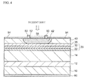
- Fig. 4 is a cross-sectional view of a semiconductor light-receiving device in accordance with a second embodiment.
- An n + -type InP dope layer 36 is provided on the electric field drop layer 32 in addition to the structure of the first embodiment shown in Fig. 2.
- the window layer 40 is provided on the dope layer 36.
- the p + -type conduction region 42 is provided so as to contact the dope layer 36. That is, the thickness of the p + -type conduction region 42 is approximately equal to the thickness of the window layer 40.
- the other structures of the second embodiment are the same as corresponding those of the first embodiment. Therefore, parts that are the same as those shown in the previous figures are given the same reference numerals, and a description thereof will be omitted here.
- Fig. 5 is a graph that explains advantages of the second embodiment.
- the horizontal axis of the graph denotes the depth from the surface of the window layer 40, and the vertical axis denotes the dope concentration below the light-receiving region 58.
- the p + -type conduction region 42 is thickened in order to increase the multiplication factor M, the p-type dope concentration has a skirt shape in a deep region from the surface.
- the p + -type conduction region 42 contacts the undoped window layer 40.
- the window layer 40 has a small amount of dose, and the sharpness of the slope of impurity concentration of the pn junction is reduced.
- the multiplication layer 20 includes the dope layer 36 of the n + -type (first conduction type), which contacts the p + -type conduction region 42 and has a dope concentration higher than that of the light absorption layer 14.
- the dope concentration of p-type forms the pn junction at a shallow position on the skirt shape.
- the pn junction with the sharp slope of the impurity concentration can be formed.
- the n + -type InP substrate 10 has an n-type carrier concentration (a silicon dopant, for example) of 2 x 10 18 cm -3 .
- the n + -type conduction layer 12 having an n-type carrier concentration of 2 x 10 18 cm -3 is formed to a thickness of 1 ⁇ m.
- the undoped light absorption layer 14 is formed to a thickness of 2 ⁇ m.
- the undoped i-InGaAsP buffer layer 22 is formed to a thickness of 0.2 ⁇ m. This is an intermediate layer in which the composition changes continuously in the thickness direction.
- the n + -type InP electric field drop layer 32 having an n-type carrier concentration of 5 x 10 17 cm -3 is formed to a thickness of 100 nm.
- the p - -type InP dope layer 36 having an n-type carrier concentration of 5 x 10 15 cm -3 is formed to a thickness of 100 nm.
- the undoped n - -type InP window layer 40 is formed to a thickness of 5.0 ⁇ m.
- the above layers may be formed by MOVPE or another crystal growing technique such as MBE.
- the avalanche multiplication starts after the edge of the depletion layer reaches a high concentration layer (the interface between the n + -type conduction layer 12 and the light absorption layer 14) (punch through).
- the depletion layer width W of expression [6] is the sum of the film thicknesses of the light absorption layer 14, the buffer layer 22, the electric field drop layer 32 and the dope layer 36, and is equal to 2.4 ⁇ m.
- the curvature radius r is, at least, X, that is, the film thickness of the undoped n - -type InP window layer 40, and is equal to 5.1 ⁇ m.
- the ratio r/W is equal to 2.13 and the condition defined by expression [6] is satisfied.
- the n + -type InP substrate 10 doped with silicon at 2 x 10 18 cm -3 is prepared.
- the following layers are formed MOVPE or MBE.
- the n + -type conduction layer 12 doped with silicon at a carrier concentration of 1 x 10 18 cm -3 is formed to a thickness of 1 ⁇ m.
- the undoped light absorption layer 14 of InGaAs is formed to a thickness of 2 ⁇ m.
- the undoped i-InGaAsP buffer layer 22 is formed to a thickness of 0.2 ⁇ m. This is an intermediate layer in which the composition changes continuously in the thickness direction.
- the n + -type InP electric field drop layer 32 doped with silicon at a carrier concentration of 5 x 10 17 cm -3 is formed to a thickness of 0.1 ⁇ m.
- the p - -type InP dope layer 36 doped with silicon at a carrier concentration of 5 x 10 15 CM -3 is formed to a thickness of 100 nm.
- the undoped n - -type InP window layer 40 is formed to a thickness of 5.1 ⁇ m.
- a silicon nitride film is formed on the window layer 40 by, for example, CVD as the protection film 54. An opening for diffusion is formed in the protection film 54 in a region corresponding to the light-receiving region 58.
- Cd or Zn is selectively diffused to form the p + -type conduction region 42 that contacts the dope layer 36.
- the antireflection layer 52 is formed in the light-receiving region.
- the p-type contact electrode 50 which has a ring shape and a two-layer structure of Au/Zn, is formed around the light-receiving region 58.
- the n-type contact electrode of AuGe is formed on the backside of the semiconductor substrate 10.
- the second embodiment is designed to prevent degradation of the slope of impurity concentration by disposing the dope layer 36 having an impurity concentration higher than that of the window layer 40 and setting the thickness of the window layer 40 equal to the depth X of the p + -type conduction region 42 so that the diffusion front of the pn junction (the center portion of the second conduction region 42) of the light-receiving region 58 coincides with the interface between the window layer 40 and the InP dope layer 36 (the diffusion front is slightly compressed to the dope layer 36).
- a required multiplication and frequency response performance in the optical fiber communication systems (in the range of 1.27 to 1.62 ⁇ m) can be obtained by setting the film thickness of the InP dope layer 36 to the range of 0.1 ⁇ m to 0.3 ⁇ m and setting the carrier concentration to the range of 5 x 10 15 cm -3 and 5 x 10 16 cm -3 .
- the curvature radius r of the arc of the edge portion 43 of the p + -type conduction region 42 is approximately equal to the thickness X of the p + -type conduction region 42.
- the curvature radius may deviate from the thickness X.
- r > X r/W becomes greater and still falls within the condition defined by expression [1].
- r ⁇ X the condition of expression [1] may not be satisfied.
- the material of the mask for diffusion may be changed.
- the mask 56 for diffusion may be changed.
- the mask 56 for diffusion may be designed to apply stress to the surface of the semiconductor layer 48, and may have a two-layer structure composed of a dielectric film such as a silicon nitride film, and a metal film having a good adhesiveness to the dielectric film such as a Ti/Pt film or a TiW film. It is thus possible to obtain a large diffusion speed in the transverse direction as compared to the mask 56 for diffusion formed by the single dielectric layer.
- the two-layer mask is removed after the p + -type conduction layer 42, and the protection film 54 is formed.
- the zone from the upper surface of the n + -type conduction layer 12 to the multiplication region adjacent to the lower surface of the p + -type conduction region 42 is depleted in operation, so that the electric field intensity necessary for avalanche multiplication can be obtained.
- Fig. 6 is a cross-sectional view of a semiconductor light-receiving device in accordance with a third embodiment.
- An n + -type InGaAs electric field drop layer 34 is provided to the structure of the first embodiment shown in Fig. 2. More specifically, the electric field drop layer 34 is interposed between the light absorption layer 14 and the buffer layer 22 and has a carrier concentration higher than that of the light absorption layer 14.
- the electric field drop layer 34 may be 0.1 ⁇ m thick and has a dope concentration of 1 x 10 16 cm -3 .
- the other structures of the third embodiment are the same as corresponding those of the first embodiment, and a description thereof will be omitted here.
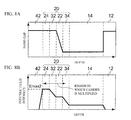
- Figs. 7A, 7B, 8A and 8B are schematic graphs for describing effects of the third embodiment as compared to the first embodiment. More particularly, Fig. 7A shows the band gaps of the semiconductor layers as a function of the depth from the surface of the p + -type conduction region 42 in the light-receiving region 58 of the APD of the first embodiment.
- the APD of the first embodiment has a large band gap because the p + -type conduction region 42, the undoped InP layer 24, the electric field drop layer 32 and the n + -type conduction layer 12 are formed by respective InP layers.
- the light absorption layer 14 is formed by an InGaAs layer that has a small band gap.
- the buffer layer 22 has the band gap that continuously changes from the InGaAs layer to the InP layer.
- Fig. 7B shows the electric field intensity as a function of the depth of the light-receiving region 58 of the APD of the first embodiment when a reverse bias is applied cross the pn junction. Since only the electric field drop layer 32 is doped with the n type in the depletion layer, the electric field mostly changes in the electric field drop layer 32. Thus, the holes (carrier) injected into the multiplication layer 20 from the light absorption layer 14 are accelerated in the electric field drop layer 32. Then, avalanche multiplication takes place in the upper portion of the electric field drop layer 32 and the undoped InP layer 24, and electrons are thus multiplied. The maximum electric field intensity necessary for obtaining the multiplication factor m is now assumed as Emax1.
- Fig. 8A shows the band gaps of the semiconductor layers as a function of the depth from the surface of the p + -type conduction region 42 in the light-receiving region 58 of the APD of the third embodiment.
- the InGaAs electric field drop layer 34 having the same band gap as that of the light absorption layer 14 is provided just above the light absorption layer 14.
- Fig. 8B shows the electric field intensity as a function of the depth of the light-receiving region 58 of the APD of the third embodiment when a reverse bias is applied cross the pn junction.
- the present APD has the two electric field drop layers doped with n + -type dopant, the electric field changes in the electric field drop layers 34 and 32.
- the holes (carrier) injected into the multiplication layer 20 from the light absorption layer 14 are accelerated in the electric field drop layer 34 first, and are accelerated in the electric field drop layer 32.
- the third embodiment has a wider multiplication region than the first embodiment.
- the third embodiment can set the maximum electric field intensity Emax2 less than the maximum electric field intensity Emax1 of the first embodiment for the same multiplication factor M. That is, the reverse bias applied across the pn junction for the same multiplication factor M can be reduced.
- the multiplication factor M is high in the InGaAs layer having a higher impact ionization rate of electrons than that of holes, excessively increased noise and degradation of the dynamic characteristics may take place. In contrast, for a multiplication factor M as low as, for example, 6, increase in nose and degradation of the dynamic characteristics may not be serious.
- the third embodiment is effective particularly to an operation with a low multiplication factor M.
- the semiconductor light-receiving device of the third embodiment has the multiplication layer 20 designed to have the electric field drop layer 34 that contacts the light absorption layer 14, the layer 34 having a narrower band gap than the p + -type conduction region 42 (second conduction region) and a higher dope concentration than the light absorption layer 14. Since the electric field drop layer 34 contacts the light absorption layer 14, the region for multiplying the carrier can be lengthened. This makes it possible to reduce the voltage applied across the pn junction for the same multiplication factor.
- the band gap of the electric field drop layer 34 is preferably identical to that of the light absorption layer 14. However, it is enough to set the band gap of the electric field drop layer 34 narrower than that of the p + -type conduction region 42.
- the film thickness of the electric field drop layer 34 equal to 5 % of the film thickness of the light absorption layer 14 in order to restrain tunnel current.
- the multiplication layer 20 may include the electric field drop layer 32 (upper electric field drop layer) that is provided above the electric field drop layer 34 through a layer (buffer layer 22) having a dope concentration lower than that of the layer 34 and has a higher dope concentration than the light absorption layer 14.
- the effective multiplication region can be expanded to a part of the light absorption layer 14, so that multiplication can be caused at a reduced voltage.
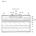
- Fig. 9 is a cross-sectional view of a semiconductor light-receiving device in accordance with a fourth embodiment.
- the fourth embodiment employs the n-type InP dope layer 36 on the electric field drop layer 32 in the third embodiment shown in Fig. 6 as in the case of the second embodiment. That is, the multiplication layer 20 includes the dope layer 36 that contacts the p + -type conduction region and has a higher cope concentration than the light absorption layer 14.
- the other structures of the fourth embodiments are the same as corresponding those of the third embodiment, and a description thereof will be omitted. According to the fourth embodiment, like the second embodiment, the sharp pn junction can be obtained in addition to the advantages of the third embodiment.
- Fig. 10 is a cross-sectional view of a semiconductor light-receiving device in accordance with a fifth embodiment.
- the fifth embodiment does not have the electric field drop layer 32 of the fourth embodiment shown in Fig. 9. That is, the electric field drop occurs in the electric field drop layer 34 only.
- the maximum electric field intensity shown in Fig. 8B can be further reduced.
- the voltage applied across the pn junction can be further reduced for the same multiplication factor M.
- Fig. 11 is a cross-sectional view of a semiconductor light-receiving device in accordance with a sixth embodiment.
- the sixth embodiment varies the structure of the fifth embodiment shown in Fig. 10 so that the sixth embodiment employs a buffer layer 26 of n - type.
- the other structures of the sixth embodiment are the same as corresponding those of the fifth embodiment, and a description thereof will be omitted.
- the buffer layer 26, which buffers the band gaps of the light absorption layer 14 made of InGaAs and the band gap of the p + -type conduction region 42 made of InP, is used as an electric field drop layer having a dope concentration greater than that of the light absorption layer 14.
- the InGaAs electric field drop layer 32 may be omitted so that the buffer layer 22 is provided directly on the light absorption layer 14 and is caused to function as the electric field drop layer.
- Fig. 12 is a cross-sectional view of a semiconductor light-receiving device in accordance with a seventh embodiment.
- the seventh embodiment differs from the third embodiment in that the seventh embodiment employs a semi-insulating InP substrate 10. Further, the p + -type conduction region 42 of the seventh embodiment is not a diffused layer but an epitaxial layer. Mesa etching is performed until it reaches the n + -type conduction layer 12, and the n-type contact electrode 60 is formed from the surface side (to which light is incident).
- the semiconductor light-receiving devices of the third through sixth embodiments may be of a mesa structure type like the seventh embodiment.
- the mesa type light-receiving structure may employ the diffusion junction or growth junction.
- the third through sixth embodiments may employ a p-type guard ring. The voltage applied across the pn junction can be reduced.
- the first and second conduction types are respectively n and p types.
- the first conduction layer is the n + -type conduction layer 12
- the second conduction region is the p + -type conduction region 42.
- the first and second conduction types may be p and n types, respectively.
- the first conduction layer is the p + -type conduction layer 12
- the second conduction region is an n + -type conduction region.
- the above-mentioned first through seventh embodiments are of a type in which light is incident to the front surface of the device. Alternatively, light may be incident to the backside or a side surface of the device.
- the first through seventh embodiments employ InP/InGaAs base semiconductor substances.
- the present invention is not limited to these semiconductor substances but may employ semiconductor substances that satisfy the relationship in size between the band gap of the multiplication layer 20 and that of the light absorption layer 14. For example, similar effects may be brought by GaAs/AlGaAs base semiconductor materials.
- the n + -type conduction layer 12 and the layer having the same band gap as that of the n + -type conduction layer 12 may be made of InP, and the light absorption layer 14 and a layer having the same band gap as that of the light absorption layer 14 may be made of InGaAs.
- the devices of the first through seventh embodiments may be used as light-receiving devices in the optical fiber communication systems.
- the electric field drop layer 32 that is formed on the light absorption layer 14 and is doped with n-type impurities and that has a thickness of 0.1 ⁇ m or less and a carrier concentration of 4 x 10 17 cm -3 .
- the product of the multiplication and band width (MB product) ranges from 20 GHz to 130 GHz
- the thickness of the undoped layer 24 is set to the range of 0.1 ⁇ m to 0.3 ⁇ m.
- the thickness of the undoped layer 24 it is possible to obtain a required quantum efficiency of 60% to 95% in the optical fiber communication systems by setting the thickness of the undoped layer 24 to the range of 0.1 ⁇ m to 0.3 ⁇ m and by setting the carrier concentration undoped or equal to 1.5 x 10 15 cm -3 or less.
- the buffer layer 22 is provided above and close to the light absorption layer 14.
- the buffer layer 22 is doped with n-type impurities or is undoped.
- the buffer layer 22 has a band gap between the n + -type conduction layer 12 and the light absorption layer 14.
- the buffer layer 22 has a thickness that ranges from 0.1 ⁇ m to 0.2 ⁇ m, and has an undoped carrier concentration or a carrier concentration of 3 ⁇ 10 15 cm -3 .
- the electric field drop layer 32 is not employed and is provided above and close to the light absorption layer 14.
- the buffer layer 26 is doped with n-type impurities or undoped.
- the buffer layer 26 has a band gap between the n + -type conduction layer 12 and the light absorption layer 14.
- the buffer layer 26 has a thickness that ranges from 0.1 ⁇ m to 0.2 ⁇ m, and is undoped or doped at a carrier concentration that ranges from 3 x 10 15 cm -3 to 3 x 10 17 cm -3 .
- the first through seventh embodiments may be used as light-receiving devices operable in a voltage environment equivalent to that of the PIN-PD (with a simple drive circuit).
- a semiconductor light-receiving device including: a first conduction layer of a first conduction type; a light absorption layer provided on the first conduction layer; a multiplication layer provided on the light absorption layer; a window layer provided on the multiplication layer, the window layer being undoped or having the first conduction type; and a second conduction region provided in the window layer by impurity diffusion, the second conduction region having a band gap wider than that of the light absorption layer and having a second conduction type different from the first conduction type.
- X / W ⁇ ( M - 1 ⁇ ) 2 / 2 ⁇ M where W is a film thickness from a lower surface of the light absorption layer and an upper surface of the multiplication layer, X is a film thickness of the second conduction region, and M is a multiplication factor.
- a part of the light absorption layer is designed to have a high impurity concentration so that a graded carrier concentration region capable of not only absorbing light but also performing multiplication can be formed.
- the APD of the present invention may be applied to less-expensive subscriber systems without expensive design modification that may include the use of a high voltage power source and a bias voltage control apparatus. Thus, the APD of the present invention may provide great economic advantages.
Landscapes
- Light Receiving Elements (AREA)
Applications Claiming Priority (1)
| Application Number | Priority Date | Filing Date | Title |
|---|---|---|---|
| JP2006141989A JP5015494B2 (ja) | 2006-05-22 | 2006-05-22 | 半導体受光素子 |
Publications (1)
| Publication Number | Publication Date |
|---|---|
| EP1860703A1 true EP1860703A1 (de) | 2007-11-28 |
Family
ID=38458062
Family Applications (1)
| Application Number | Title | Priority Date | Filing Date |
|---|---|---|---|
| EP07108665A Withdrawn EP1860703A1 (de) | 2006-05-22 | 2007-05-22 | Lichtsensitives Halbleiterbauelement mit Ladungsträgervervielfachung |
Country Status (4)
| Country | Link |
|---|---|
| US (1) | US20070267653A1 (de) |
| EP (1) | EP1860703A1 (de) |
| JP (1) | JP5015494B2 (de) |
| CN (1) | CN100492674C (de) |
Families Citing this family (16)
| Publication number | Priority date | Publication date | Assignee | Title |
|---|---|---|---|---|
| JP2009010175A (ja) * | 2007-06-28 | 2009-01-15 | Sumitomo Electric Ind Ltd | 受光素子およびその製造方法 |
| JP2012248655A (ja) * | 2011-05-27 | 2012-12-13 | Mitsubishi Electric Corp | アバランシェフォトダイオード及びアバランシェフォトダイオードアレイ |
| US8368159B2 (en) * | 2011-07-08 | 2013-02-05 | Excelitas Canada, Inc. | Photon counting UV-APD |
| US9893227B2 (en) * | 2013-05-24 | 2018-02-13 | The United States Of America As Represented By The Secretary Of The Army | Enhanced deep ultraviolet photodetector and method thereof |
| US9318639B2 (en) * | 2013-09-17 | 2016-04-19 | Finisar Corporation | Gallium arsenide avalanche photodiode |
| CN104900748B (zh) * | 2015-04-21 | 2017-03-01 | 中国电子科技集团公司第四十四研究所 | 一种具有不等光电口径的垂直进光雪崩光电二极管 |
| US10381502B2 (en) * | 2015-09-09 | 2019-08-13 | Teledyne Scientific & Imaging, Llc | Multicolor imaging device using avalanche photodiode |
| JP6710343B2 (ja) * | 2017-09-15 | 2020-06-17 | 三菱電機株式会社 | 半導体受光素子およびその製造方法 |
| JP6860467B2 (ja) * | 2017-10-26 | 2021-04-14 | ソニーセミコンダクタソリューションズ株式会社 | フォトダイオード、画素回路、および、フォトダイオードの製造方法 |
| JP6641442B1 (ja) * | 2018-10-16 | 2020-02-05 | 浜松ホトニクス株式会社 | 光検出素子及び光検出装置 |
| CN110544731B (zh) * | 2019-09-05 | 2021-06-15 | 中国电子科技集团公司第十三研究所 | 一种紫外探测器及其制备方法 |
| CN114792738B (zh) * | 2021-01-26 | 2025-04-18 | 朗美通日本株式会社 | 半导体光接收元件 |
| CN113921646B (zh) * | 2021-09-30 | 2023-03-31 | 厦门市三安集成电路有限公司 | 单光子探测器及其制作方法、单光子探测器阵列 |
| US12527118B1 (en) * | 2022-02-03 | 2026-01-13 | Aeluma, Inc. | Sensor array device and method therefor |
| JP7799548B2 (ja) * | 2022-04-15 | 2026-01-15 | キヤノン株式会社 | 光電変換素子及び光電変換装置 |
| WO2024154204A1 (ja) * | 2023-01-16 | 2024-07-25 | 三菱電機株式会社 | 裏面入射型受光素子 |
Citations (14)
| Publication number | Priority date | Publication date | Assignee | Title |
|---|---|---|---|---|
| US4083062A (en) * | 1976-02-21 | 1978-04-04 | Hitachi, Ltd. | Avalanche photodiode with reduced avalanche breakdown voltage |
| US4587544A (en) * | 1984-04-10 | 1986-05-06 | Rca Inc. | Avalanche photodetector |
| JPS6233482A (ja) * | 1985-08-07 | 1987-02-13 | Mitsubishi Electric Corp | アバランシエホトダイオ−ド |
| EP0325532A2 (de) * | 1988-01-18 | 1989-07-26 | Fujitsu Limited | Halbleiterphotodiode |
| JPH01261874A (ja) * | 1988-04-13 | 1989-10-18 | Hitachi Ltd | 光検出器 |
| JPH03255676A (ja) * | 1989-06-07 | 1991-11-14 | Mitsubishi Electric Corp | アバランシエフオトダイオードの製造方法 |
| US5654578A (en) * | 1994-12-22 | 1997-08-05 | Nec Corporation | Superlattice avalanche photodiode with mesa structure |
| JPH1065202A (ja) * | 1996-06-29 | 1998-03-06 | Hyundai Electron Ind Co Ltd | アバランシェフォトダイオード及びその製造方法 |
| US6515315B1 (en) * | 1999-08-05 | 2003-02-04 | Jds Uniphase, Corp. | Avalanche photodiode for high-speed applications |
| US20030111675A1 (en) * | 2001-11-27 | 2003-06-19 | Jds Uniphase Corporation | Doped absorption for enhanced responsivity for high speed photodiodes |
| WO2003065417A2 (en) * | 2002-02-01 | 2003-08-07 | Picometrix, Inc. | Charge controlled avalanche photodiode and method of making the same |
| US20040245592A1 (en) * | 2003-05-01 | 2004-12-09 | Yale University | Solid state microchannel plate photodetector |
| US20060001118A1 (en) * | 2004-06-30 | 2006-01-05 | Boisvert Joseph C | Low capacitance avalanche photodiode |
| US20070085158A1 (en) * | 2005-10-17 | 2007-04-19 | Princeton Lightwave, Inc. | Apparatus comprising an avalanche photodiode |
Family Cites Families (11)
| Publication number | Priority date | Publication date | Assignee | Title |
|---|---|---|---|---|
| JPS5793585A (en) * | 1980-12-02 | 1982-06-10 | Fujitsu Ltd | Semiconductor photoreceiving element |
| JPS61172381A (ja) * | 1984-12-22 | 1986-08-04 | Fujitsu Ltd | InP系化合物半導体装置 |
| JPH0821727B2 (ja) * | 1988-11-18 | 1996-03-04 | 日本電気株式会社 | アバランシェフォトダイオード |
| JPH02159775A (ja) * | 1988-12-14 | 1990-06-19 | Toshiba Corp | 半導体受光素子及びその製造方法 |
| JP2937404B2 (ja) * | 1990-04-18 | 1999-08-23 | 日本電気株式会社 | 半導体受光素子 |
| JP2682253B2 (ja) * | 1991-04-18 | 1997-11-26 | 三菱電機株式会社 | アバランシェ・フォトダイオード及びその製造方法 |
| US6359322B1 (en) * | 1999-04-15 | 2002-03-19 | Georgia Tech Research Corporation | Avalanche photodiode having edge breakdown suppression |
| JP2002231992A (ja) * | 2001-02-02 | 2002-08-16 | Toshiba Corp | 半導体受光素子 |
| JP4157698B2 (ja) * | 2001-11-26 | 2008-10-01 | ユーディナデバイス株式会社 | 半導体受光素子およびその駆動方法 |
| US7202102B2 (en) * | 2001-11-27 | 2007-04-10 | Jds Uniphase Corporation | Doped absorption for enhanced responsivity for high speed photodiodes |
| JP2005093610A (ja) * | 2003-09-16 | 2005-04-07 | Sumitomo Electric Ind Ltd | 光受信器 |
-
2006
- 2006-05-22 JP JP2006141989A patent/JP5015494B2/ja not_active Expired - Fee Related
-
2007
- 2007-05-21 US US11/751,292 patent/US20070267653A1/en not_active Abandoned
- 2007-05-22 EP EP07108665A patent/EP1860703A1/de not_active Withdrawn
- 2007-05-22 CN CNB2007101040769A patent/CN100492674C/zh not_active Expired - Fee Related
Patent Citations (14)
| Publication number | Priority date | Publication date | Assignee | Title |
|---|---|---|---|---|
| US4083062A (en) * | 1976-02-21 | 1978-04-04 | Hitachi, Ltd. | Avalanche photodiode with reduced avalanche breakdown voltage |
| US4587544A (en) * | 1984-04-10 | 1986-05-06 | Rca Inc. | Avalanche photodetector |
| JPS6233482A (ja) * | 1985-08-07 | 1987-02-13 | Mitsubishi Electric Corp | アバランシエホトダイオ−ド |
| EP0325532A2 (de) * | 1988-01-18 | 1989-07-26 | Fujitsu Limited | Halbleiterphotodiode |
| JPH01261874A (ja) * | 1988-04-13 | 1989-10-18 | Hitachi Ltd | 光検出器 |
| JPH03255676A (ja) * | 1989-06-07 | 1991-11-14 | Mitsubishi Electric Corp | アバランシエフオトダイオードの製造方法 |
| US5654578A (en) * | 1994-12-22 | 1997-08-05 | Nec Corporation | Superlattice avalanche photodiode with mesa structure |
| JPH1065202A (ja) * | 1996-06-29 | 1998-03-06 | Hyundai Electron Ind Co Ltd | アバランシェフォトダイオード及びその製造方法 |
| US6515315B1 (en) * | 1999-08-05 | 2003-02-04 | Jds Uniphase, Corp. | Avalanche photodiode for high-speed applications |
| US20030111675A1 (en) * | 2001-11-27 | 2003-06-19 | Jds Uniphase Corporation | Doped absorption for enhanced responsivity for high speed photodiodes |
| WO2003065417A2 (en) * | 2002-02-01 | 2003-08-07 | Picometrix, Inc. | Charge controlled avalanche photodiode and method of making the same |
| US20040245592A1 (en) * | 2003-05-01 | 2004-12-09 | Yale University | Solid state microchannel plate photodetector |
| US20060001118A1 (en) * | 2004-06-30 | 2006-01-05 | Boisvert Joseph C | Low capacitance avalanche photodiode |
| US20070085158A1 (en) * | 2005-10-17 | 2007-04-19 | Princeton Lightwave, Inc. | Apparatus comprising an avalanche photodiode |
Non-Patent Citations (1)
| Title |
|---|
| WATANABE I ET AL: "IMPACT IONIZATION RATES IN (100) AL0.48IN0.52AS", IEEE ELECTRON DEVICE LETTERS, IEEE SERVICE CENTER, NEW YORK, NY, US, vol. 11, no. 10, 1 October 1990 (1990-10-01), pages 437 - 438, XP000148546, ISSN: 0741-3106 * |
Also Published As
| Publication number | Publication date |
|---|---|
| CN101079453A (zh) | 2007-11-28 |
| JP2007311720A (ja) | 2007-11-29 |
| US20070267653A1 (en) | 2007-11-22 |
| CN100492674C (zh) | 2009-05-27 |
| JP5015494B2 (ja) | 2012-08-29 |
Similar Documents
| Publication | Publication Date | Title |
|---|---|---|
| EP1860703A1 (de) | Lichtsensitives Halbleiterbauelement mit Ladungsträgervervielfachung | |
| US7348608B2 (en) | Planar avalanche photodiode | |
| EP0675549B1 (de) | Lawinenphotodiode mit Übergitter | |
| EP3229279B1 (de) | Lawinenphotodiode | |
| EP1811578B1 (de) | Avalanche-fotodiode | |
| EP2378567B1 (de) | Lawinenphotodiode | |
| JP3996699B2 (ja) | 半導体光検出器 | |
| EP0156156A1 (de) | Avalanche-Photodioden | |
| KR900004180B1 (ko) | 반도체 광검지기 및 그 제조방법 | |
| EP0043734A2 (de) | Avalanche-Fotodioden | |
| US7582920B2 (en) | Apparatus comprising an avalanche photodiode | |
| US20100133637A1 (en) | Avalanche photodiode | |
| EP2613365B1 (de) | Lawinenphotodiode | |
| JP2000323746A (ja) | アバランシェフォトダイオードとその製造方法 | |
| CN100541721C (zh) | 平面型雪崩光电二极管 | |
| JP5303793B2 (ja) | フォトダイオード | |
| EP0150564A2 (de) | Elektronische Vorrichtung mit einem Heteroübergang | |
| US20070087511A1 (en) | Method for forming an avalanche photodiode | |
| KR0164094B1 (ko) | 부분적으로 높은 전하층을 갖는 애벌랜치 포토다이오드 및 그의 제조방법 | |
| JPH0281480A (ja) | 半導体受光素子 | |
| HK1113520B (en) | Planar avalanche photodiode |
Legal Events
| Date | Code | Title | Description |
|---|---|---|---|
| PUAI | Public reference made under article 153(3) epc to a published international application that has entered the european phase |
Free format text: ORIGINAL CODE: 0009012 |
|
| AK | Designated contracting states |
Kind code of ref document: A1 Designated state(s): AT BE BG CH CY CZ DE DK EE ES FI FR GB GR HU IE IS IT LI LT LU LV MC MT NL PL PT RO SE SI SK TR |
|
| AX | Request for extension of the european patent |
Extension state: AL BA HR MK YU |
|
| 17P | Request for examination filed |
Effective date: 20080527 |
|
| AKX | Designation fees paid |
Designated state(s): DE FR GB |
|
| 17Q | First examination report despatched |
Effective date: 20080715 |
|
| STAA | Information on the status of an ep patent application or granted ep patent |
Free format text: STATUS: THE APPLICATION IS DEEMED TO BE WITHDRAWN |
|
| 18D | Application deemed to be withdrawn |
Effective date: 20121201 |