EP1860733A1 - Elément d'absorption pour rayonnement électromagnétique à haute fréquence - Google Patents
Elément d'absorption pour rayonnement électromagnétique à haute fréquence Download PDFInfo
- Publication number
- EP1860733A1 EP1860733A1 EP07010006A EP07010006A EP1860733A1 EP 1860733 A1 EP1860733 A1 EP 1860733A1 EP 07010006 A EP07010006 A EP 07010006A EP 07010006 A EP07010006 A EP 07010006A EP 1860733 A1 EP1860733 A1 EP 1860733A1
- Authority
- EP
- European Patent Office
- Prior art keywords
- element according
- absorption element
- radiation
- reflection
- antenna
- Prior art date
- Legal status (The legal status is an assumption and is not a legal conclusion. Google has not performed a legal analysis and makes no representation as to the accuracy of the status listed.)
- Granted
Links
- 238000010521 absorption reaction Methods 0.000 title claims description 46
- 230000005855 radiation Effects 0.000 claims abstract description 48
- 239000004020 conductor Substances 0.000 claims description 16
- 230000005670 electromagnetic radiation Effects 0.000 claims description 10
- 230000002745 absorbent Effects 0.000 claims description 8
- 239000002250 absorbent Substances 0.000 claims description 8
- 238000000034 method Methods 0.000 claims description 6
- 239000002184 metal Substances 0.000 claims description 4
- 238000007650 screen-printing Methods 0.000 claims description 3
- 238000007639 printing Methods 0.000 claims description 2
- 230000005404 monopole Effects 0.000 abstract description 2
- 230000010287 polarization Effects 0.000 description 6
- 230000005540 biological transmission Effects 0.000 description 2
- 238000001514 detection method Methods 0.000 description 2
- 238000005516 engineering process Methods 0.000 description 2
- 241000143290 Idaea belemiata Species 0.000 description 1
- 239000000853 adhesive Substances 0.000 description 1
- 230000001070 adhesive effect Effects 0.000 description 1
- 230000033228 biological regulation Effects 0.000 description 1
- 238000006243 chemical reaction Methods 0.000 description 1
- 238000010276 construction Methods 0.000 description 1
- 230000008878 coupling Effects 0.000 description 1
- 238000010168 coupling process Methods 0.000 description 1
- 238000005859 coupling reaction Methods 0.000 description 1
- 230000005684 electric field Effects 0.000 description 1
- 230000005672 electromagnetic field Effects 0.000 description 1
- 239000000463 material Substances 0.000 description 1
- 230000001902 propagating effect Effects 0.000 description 1
- 238000005096 rolling process Methods 0.000 description 1
- 238000007493 shaping process Methods 0.000 description 1
- 230000000007 visual effect Effects 0.000 description 1
Images


Classifications
-
- H—ELECTRICITY
- H01—ELECTRIC ELEMENTS
- H01Q—ANTENNAS, i.e. RADIO AERIALS
- H01Q17/00—Devices for absorbing waves radiated from an antenna; Combinations of such devices with active antenna elements or systems
- H01Q17/008—Devices for absorbing waves radiated from an antenna; Combinations of such devices with active antenna elements or systems with a particular shape
-
- H—ELECTRICITY
- H01—ELECTRIC ELEMENTS
- H01Q—ANTENNAS, i.e. RADIO AERIALS
- H01Q17/00—Devices for absorbing waves radiated from an antenna; Combinations of such devices with active antenna elements or systems
- H01Q17/001—Devices for absorbing waves radiated from an antenna; Combinations of such devices with active antenna elements or systems for modifying the directional characteristic of an aerial
-
- H—ELECTRICITY
- H01—ELECTRIC ELEMENTS
- H01Q—ANTENNAS, i.e. RADIO AERIALS
- H01Q17/00—Devices for absorbing waves radiated from an antenna; Combinations of such devices with active antenna elements or systems
- H01Q17/002—Devices for absorbing waves radiated from an antenna; Combinations of such devices with active antenna elements or systems using short elongated elements as dissipative material, e.g. metallic threads or flake-like particles
Definitions
- the invention relates to an absorption element for electromagnetic high-frequency radiation, in particular for radiation, as used in the RFID (Radio Frequency Identification) area.
- RFID Radio Frequency Identification
- RFID is a technology for non-contact automatic identification of objects via radio detection.
- data stored on so-called transponders are read without contact and without visual contact.
- Such transponders can be attached to objects, which are then automatically and quickly identifiable based on the data stored thereon.
- An RFID reading system stimulates the transponder to transmit the data stored on the transponder by emitting electromagnetic radiation. This technology can be used anywhere where objects must be automatically identified, detected, registered, stored, monitored or transported.
- the strength of the fields or the frequencies are determined by national and international regulations. For example, for the UHF range, depending on the country and approval, three to approx. Ten different frequencies are allowed for transmission between transponder and RFID reading system. In certain applications, it is necessary that several such RFID registrations are performed in a comparatively small space. There is no interference between the individual applications as long as different frequencies can be used. However, due to the limited number of available frequencies, it may be the case that for different applications, the same frequency must be used for transmission between the transponder and the RFID reading system, although the radiation fields generated in the applications spatially overlap. This, in turn, may result in the aforementioned disturbances, which ultimately may at least degrade the reliability of the registration, or may jeopardize the simultaneous feasibility of all applications.
- a possible solution to this problem may be that the performance of the RFID reading system is adapted to the respective range required. However, this requires an intervention in the electrical circuit of the RFID reading system or requires an increased circuit complexity.
- the invention has the object, at least partially remedy the problem described in the use of RFID registration.
- the absorption element has a curved reflecting surface reflecting device with a plurality of sections focusing the high-frequency radiation for producing a plurality of regions with increased field strength in front of the reflecting device and a plurality of antenna circuit arrangements adapted to the frequency of the radiation each having an antenna conductor structure for receiving radiation energy and a means for converting the absorbed radiation energy into another form of energy.
- the propagation into such areas of space can be avoided, in which radiation of the same frequency is used for an RFID registration, so that ultimately a mutual interference of the different RFID applications is prevented.
- electromagnetic radiation can be prevented from propagating into regions in which this is undesirable.
- the invention is based on the idea of preventing the propagation of electromagnetic high-frequency radiation into certain areas of space by providing a device which, on the one hand, reflects the radiation but, moreover, also ensures that the radiation is absorbed, i. is converted into another form of energy, so that no interference by multiply reflected high frequency radiation can occur.
- High-frequency radiation and thermal radiation are considered as different forms of energy.
- an antenna circuit arrangement may be arranged in front of the reflection device in a region of increased field strength, so that the radiation is picked up by the antenna circuit arrangement with high efficiency.
- the means for converting the absorbed radiant energy to generate thermal energy is formed and may, for example, comprise a resistor which is connected to the antenna conductor structure.
- the means for conversion the absorbed radiation energy comprise an electroluminescent emitter, such as a light emitting diode, which is connected to the antenna conductor structure.
- the radiant energy received by the antenna is converted into electrical energy, which in turn is converted into either IR radiation or visible radiation.
- the user can visually display the effectiveness of the absorption element according to the invention.
- an antenna circuit arrangement is arranged in a region of increased field strength in front of the reflection device such that the antenna conductor structure is aligned with the focused radiation.
- the antenna structure can be adapted to the field strength profile in the areas with increased field strength.
- the reflective surface i. the surface of the reflection device has a wave structure, in particular a plane wave structure.
- the reflection surface on mountains and valleys, which run on straight lines.
- Such a wave structure may be formed as a kind of juxtaposition of a plurality of cylindrical lenses for electromagnetic radiation.
- the reflection surface of the reflection device comprises mutually adjacent different wave structure regions, the wave troughs or wave peaks of adjacent wave structure regions are arranged perpendicular to each other.
- the antenna conductor structure of the antenna circuit arrangements may be provided in the form of a dipole structure.
- a dipoleite structure is particularly well suited to the fields generated by the described wave structure regions of the reflection surface. It may be expedient if the axis of the dipole structure is placed parallel to a wave crest or a wave trough of the wave structure at the reflection surface of the reflection means, i. that the Dipolleiter Quilt is aligned with the wave structure of the reflection surface.
- the coupling of the radiation into the antenna conductor structure can be increased if the distance between the antenna conductor structure and the reflection surface is a predetermined distance. It may be expedient if this distance is equal to an odd multiple of half the wavelength of the high-frequency radiation. This ensures that the radiation reflected by the reflection surface of the reflection device is constructively superimposed on the incident radiation at the location of the antenna conductor structure.
- antenna circuit arrangements are provided on both sides of the reflection device, so that incident radiation from both sides can be eliminated by the absorption element according to the invention.
- the reflection device comprises a metal sheet or a wire mesh.
- a metal sheet or braid With such a metal sheet or braid, it is possible in a simple manner to produce advantageous surface structures, in particular the wave structure regions mentioned above, by means of known shaping techniques.
- the surface structure of the reflection device it can be provided that at least the two main surfaces of the reflection device are each covered by a plate-shaped device.
- the necessary condition is that the plate-shaped element or the plate-shaped device comprises a material which transmits the radiation to be absorbed and in particular does not have a high degree of reflection for the electromagnetic radiation.
- the covering device can in particular rest directly on the reflection device, so that the wave troughs or mountains are supported on the two covering devices.
- the antenna circuit arrangements may be arranged on the surface of the covering device, as a result of which they can be arranged in a particularly simple manner in a location-specific manner, for example via a printing process such as a screen printing process.
- the absorption element according to the invention can in principle be produced with any desired dimensions. It may be advantageous if the element is stackable, so that starting from the size of the absorption element arbitrarily large absorption surfaces or walls can be generated. It is expedient if the absorption element according to the invention is designed to be manually transportable in its dimensions or its weight.
- Fig. 1 is an application situation for an inventive Absorption element 1, 2, 3, 4 shown.
- the figure shows an outer hall wall 30, in which spaced apart two roller doors 31a, 31b are arranged.
- These gates can be approached, for example, by a truck, such that the loading area is aligned with the gate.
- a transport such as a forklift, which moves through the respective gate in the back of the truck, objects can be picked up and introduced through the said gate in the hall.
- these objects are each provided with a transponder, which is detected by an RFID reading system placed in the area of the door.
- a transponder 22a, 22b which in each case comprises a transponder antenna 23a, b, is shown by way of example in each of the gates 31a, 31b.
- the respective transponder enters the effective range of the RFID reading device 20a, 20b, which respectively has an RFID antenna 21a, 21b, the respective transponder is detected and registered by the system. If both gates are used at the same time for introduction into the hall of goods marked with a transponder, the electromagnetic fields generated by the data exchange between the RFID reading system 20a and the associated transponder 22a or the RFID reading system 20b and the associated transponder 22b are generated, disturb. Such a disturbance occurs in particular when the RFID recognition systems operate at the same frequencies.
- One or more of the absorption elements according to the invention can be used to remedy these disorders.
- four elements 1-4 are shown in the interior of the hall, of which two are stacked on top of each other, such that they extend approximately perpendicular to the hall wall 30 in the hall interior. If, for example, from the antenna 21a of the RFID reading system 20a electromagnetic high-frequency radiation in the direction of the adjacent RFID reading system 20b or whose antenna 21b is radiated, this radiation is reflected and absorbed by the absorption elements 1, 2 arranged as shown, so that this radiation can not lead to erroneous detections. As shown in FIG. 1, it may be particularly expedient to set up such absorption elements 3, 4 on the second door 31b, so that all door detectors are decoupled with respect to the gate-specific electromagnetic radiation.
- FIG. 2 a shows a thin metal sheet 40, which comprises a planar wave structure with wave crests 42 and wave troughs 41, wherein the wave troughs or wave crests respectively extend on a straight line.
- the sheet will focus for incident high frequency electromagnetic radiation through the curved sections so that areas of increased field strength are formed in front of the sheet after reflection of the radiation.
- dipole antennas according to the invention are arranged in a manner to be described, see FIG. 2 b, which shows such a dipole antenna 50. It comprises two monopolies 51, 52 as antenna conductor structures, wherein at the base of a matched to the impedance of the dipole loss resistor 53 is arranged, which connects both monopolies 51, 52 to each other electrically.
- the dipole has an electrical length L corresponding to an odd multiple of ⁇ / 2, where ⁇ is the wavelength of the electromagnetic high frequency radiation.
- the radiation field comprises UHF with a wavelength of 30 cm.
- the plane wave structure of the reflection plate 40 has the property of cylinder lenses arranged next to one another, inasmuch as the dipole antenna indicated in FIG. 2b is adapted to the regions of increased field strength generated by the reflection plate 40.
- the antenna shown in Fig. 2b takes the electromagnetic High frequency field, wherein the absorbed energy is converted by means of the impedance matched resistor 53 into thermal energy.
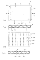
- Fig. 3 shows an inventive absorption element in an overview.
- the element 1 is of cuboid construction, the main surfaces being provided by two main cover plates 60, 61.
- the two longitudinal surfaces are formed by the side deck plates 62, 63, while the two end faces are provided by the side deck plates 64, 65.
- the side surfaces serve as a standing surface, so that the absorption element shown in Fig. 3 is also stackable.
- FIG. 4 shows the absorption element 1 shown in FIG. 3 in a sectional view along the lines IV-IV.
- the wave-shaped reflection plate 40 extends between the main cover plates 60, 61 over the entire surface thereof. In each case spaced from a wave trough dipole antennas 50a, 50b are arranged on both sides of the reflective plate 40.
- Reference symbol S denotes a region of the sectional view, which is shown in detail in FIG. 5.
- the wave structure in the described embodiment is composed of cylinder jacket segments, the radius of the cylinder segments being equal to R.
- the distance of the antennas, here the antenna 50b, to the wave trough is A.
- the distance of all dipole antennas to the respective associated trough is the same in the described embodiment.
- the distance A can be, for example, equal to half the radius of curvature, ie R / 2.
- M indicates in the drawing the center point for the curvature with the radius R.
- the distance A is set to (n + 1) ⁇ ⁇ ⁇ / 2, where n is a natural number is.
- Fig. 6 shows the absorption element according to the invention shown in Fig. 1 in a sectional view along the lines VI-VI, which runs parallel to one of the main cover plates 60 and 61, respectively.
- the front dipole antennas 50a and the rear dipole antennas 50b are offset from each other relative to a plane parallel to the main top plates 60, 61, so that only the rear dipole antennas 50b are in the illustrated plane in FIG.
- all the antennas 50a, 50b are electrically independent of each other, they each comprise only as described the two coordinated monopolies, which are connected to one another at the base via the resistor 53, see FIG.
- FIG. 7 corresponds to the sectional illustration of an absorption element shown in FIG. 4, but here the front-side antennas 50b and rear-side antennas 50a are placed at a different distance from the associated wave trough, such that they are arranged on the respective rear side of the two main cover plates 60, 61 issue.
- the distance between the respective dipole antenna and the associated trough is 2R in the example shown in FIG. 7, where R corresponds to the radius of curvature of such a wave trough.
- the arrangement of the antennas is relatively easy to accomplish, for example, the described antenna circuit arrangements can be printed on the back of the plates 60, 61.
- the two monopoles can be applied, in particular via a screen-printing process, and subsequently the resistor adapted to the impedance can be glued in with a conductive adhesive.
- the embodiments described so far are adapted to the absorption of electromagnetic high-frequency radiation of a predetermined polarization. Since in the reflection of electromagnetic radiation on metallic surfaces a Polarization rotation occurs by 90 °, it may be very advantageous if the absorption element according to the invention for absorbing electromagnetic high frequency radiation of different polarization is formed.
- Figures 8a and 8b show sections corresponding to those shown in Figures 4 and 6 by such, polarization independently working absorption element. Sections with perpendicular dipole antennas alternate with sections where the dipoles are oriented horizontally, see Figure 8b.
- an absorption element designed in this way captures and absorbs radiation with horizontal as well as radiation with vertical polarization.
- the wave structure of the reflection plate is adapted to the course of the dipole antennas. This means that in the sections in which the dipoles extend vertically, the wave structure is formed, for example, as indicated in FIG. 4. However, in those sections where the dipoles are horizontal, the wave structure is rotated 90 ° to the wave structure of the previous section, i. Wave troughs and wave crests also run there on horizontal straight lines, see FIG. 8a.
- antenna circuit arrangements which comprise an antenna dipole, wherein the reflection means is adapted to the geometry of the dipole antennas by means of the described wave structure.
- other antenna structures may be used, to which then the curvature of the reflection means is adapted.
- the absorption element according to the invention can be used in principle for all applications in which electromagnetic interference is to be destroyed.
Landscapes
- Aerials With Secondary Devices (AREA)
- Variable-Direction Aerials And Aerial Arrays (AREA)
- Inorganic Insulating Materials (AREA)
- Control Of Motors That Do Not Use Commutators (AREA)
- Shielding Devices Or Components To Electric Or Magnetic Fields (AREA)
Applications Claiming Priority (1)
| Application Number | Priority Date | Filing Date | Title |
|---|---|---|---|
| DE202006008437U DE202006008437U1 (de) | 2006-05-24 | 2006-05-24 | Absorptionselement für elektromagnetische Hochfrequenzstrahlung |
Publications (2)
| Publication Number | Publication Date |
|---|---|
| EP1860733A1 true EP1860733A1 (fr) | 2007-11-28 |
| EP1860733B1 EP1860733B1 (fr) | 2010-04-14 |
Family
ID=38290028
Family Applications (1)
| Application Number | Title | Priority Date | Filing Date |
|---|---|---|---|
| EP07010006A Not-in-force EP1860733B1 (fr) | 2006-05-24 | 2007-05-19 | Elément d'absorption pour rayonnement électromagnétique à haute fréquence |
Country Status (3)
| Country | Link |
|---|---|
| EP (1) | EP1860733B1 (fr) |
| AT (1) | ATE464675T1 (fr) |
| DE (2) | DE202006008437U1 (fr) |
Cited By (2)
| Publication number | Priority date | Publication date | Assignee | Title |
|---|---|---|---|---|
| EP3089269A1 (fr) * | 2015-04-30 | 2016-11-02 | Airbus Operations (S.A.S.) | Dispositif d'absorption d'ondes electromagnetiques destine a etre fixe sur une paroi |
| CN115460902A (zh) * | 2022-09-30 | 2022-12-09 | 紫光计算机科技有限公司 | 电磁辐射的消除方法及消除装置、电子设备 |
Citations (3)
| Publication number | Priority date | Publication date | Assignee | Title |
|---|---|---|---|---|
| US4482897A (en) | 1982-06-28 | 1984-11-13 | At&T Bell Laboratories | Multibeam segmented reflector antennas |
| GB2251338A (en) * | 1985-10-15 | 1992-07-01 | Secr Defence | Microwave absorber |
| WO1994024724A1 (fr) | 1993-04-09 | 1994-10-27 | Chomerics, Inc. | Absorbeur d'energie electromagnetique a large bande |
Family Cites Families (2)
| Publication number | Priority date | Publication date | Assignee | Title |
|---|---|---|---|---|
| US3599210A (en) * | 1969-11-18 | 1971-08-10 | Us Navy | Radar absorptive coating |
| US5325094A (en) * | 1986-11-25 | 1994-06-28 | Chomerics, Inc. | Electromagnetic energy absorbing structure |
-
2006
- 2006-05-24 DE DE202006008437U patent/DE202006008437U1/de not_active Expired - Lifetime
-
2007
- 2007-05-19 AT AT07010006T patent/ATE464675T1/de active
- 2007-05-19 EP EP07010006A patent/EP1860733B1/fr not_active Not-in-force
- 2007-05-19 DE DE502007003440T patent/DE502007003440D1/de active Active
Patent Citations (3)
| Publication number | Priority date | Publication date | Assignee | Title |
|---|---|---|---|---|
| US4482897A (en) | 1982-06-28 | 1984-11-13 | At&T Bell Laboratories | Multibeam segmented reflector antennas |
| GB2251338A (en) * | 1985-10-15 | 1992-07-01 | Secr Defence | Microwave absorber |
| WO1994024724A1 (fr) | 1993-04-09 | 1994-10-27 | Chomerics, Inc. | Absorbeur d'energie electromagnetique a large bande |
Cited By (4)
| Publication number | Priority date | Publication date | Assignee | Title |
|---|---|---|---|---|
| EP3089269A1 (fr) * | 2015-04-30 | 2016-11-02 | Airbus Operations (S.A.S.) | Dispositif d'absorption d'ondes electromagnetiques destine a etre fixe sur une paroi |
| FR3035742A1 (fr) * | 2015-04-30 | 2016-11-04 | Airbus Operations Sas | Dispositif d'absorption d'ondes electromagnetiques destine a etre fixe sur une paroi |
| US9991603B2 (en) | 2015-04-30 | 2018-06-05 | Airbus Operations (Sas) | Device, intended to be fixed on a wall, for absorbing electromagnetic waves |
| CN115460902A (zh) * | 2022-09-30 | 2022-12-09 | 紫光计算机科技有限公司 | 电磁辐射的消除方法及消除装置、电子设备 |
Also Published As
| Publication number | Publication date |
|---|---|
| ATE464675T1 (de) | 2010-04-15 |
| EP1860733B1 (fr) | 2010-04-14 |
| DE202006008437U1 (de) | 2007-09-27 |
| DE502007003440D1 (de) | 2010-05-27 |
Similar Documents
| Publication | Publication Date | Title |
|---|---|---|
| EP2176681B1 (fr) | Radar détecteur pour véhicules automobiles | |
| DE602004006348T2 (de) | HF-Etikettenmodul und Artikel mit einem HF-Etikettenmodul | |
| DE69613244T2 (de) | Planare gruppenantenne für zwei frequenzen | |
| DE102006050344B4 (de) | Aufnahmebehälter mit RFID-Etikett | |
| DE2815453A1 (de) | Streuungsfreie ultrahochfrequenzantenne mit elektronischer ablenkung | |
| EP3918172B1 (fr) | Unité de vitrage isolant et vitrage | |
| DE2362913B2 (de) | Spiralantenne | |
| DE202022107107U1 (de) | Integrierte Basisstationsantenne | |
| EP1678787A1 (fr) | Dispositif et procede permettant d'emettre et/ou de recevoir un rayonnement electromagnetique | |
| DE2427505A1 (de) | Antennensystem mit einem in offener bauweise ausgebildeten reflektor | |
| DE3217437A1 (de) | Mikrowellen-richtantenne aus einer dielektrischen leitung | |
| DE948705C (de) | Antennenanordnung fuer den Dezimeterwellenbereich | |
| EP1860733B1 (fr) | Elément d'absorption pour rayonnement électromagnétique à haute fréquence | |
| DE3027093C2 (de) | Umpolarisiereinrichtung zur Erzeugung zirkular polarisierter elektromagnetischer Wellen | |
| DE2335792A1 (de) | Funknavigations-, insbesondere landesystem | |
| DE112017000933B4 (de) | Radar mit reichweitenunabhängiger Auflösung | |
| DE3700886A1 (de) | Hohlleiterschlitzantenne fuer doppler-navigatoren | |
| DE2330654C3 (de) | Strahlerzeile, bei der das keulenförmige Strahlungsdiagramm durch Frequenzänderung schwenkbar ist | |
| WO2007131879A1 (fr) | Dispositif d'essai présentant une antenne à double bande hf-/uhf destiné à tester des transpondeurs rfid dans un dispositif de production | |
| DE518622C (de) | Mehrfachantenne | |
| DE102012101443A9 (de) | Planare Antennenanordnung | |
| DE102006062308A1 (de) | Passives Detektierplättchen | |
| DE1591040A1 (de) | Sendeantenne | |
| EP4010556A1 (fr) | Vitrage avec transpondeur d'identification par radiofréquence (rfid) | |
| DE112017005061T5 (de) | Erweiterte Antennensysteme |
Legal Events
| Date | Code | Title | Description |
|---|---|---|---|
| PUAI | Public reference made under article 153(3) epc to a published international application that has entered the european phase |
Free format text: ORIGINAL CODE: 0009012 |
|
| AK | Designated contracting states |
Kind code of ref document: A1 Designated state(s): AT BE BG CH CY CZ DE DK EE ES FI FR GB GR HU IE IS IT LI LT LU LV MC MT NL PL PT RO SE SI SK TR |
|
| AX | Request for extension of the european patent |
Extension state: AL BA HR MK YU |
|
| 17P | Request for examination filed |
Effective date: 20080527 |
|
| RAP1 | Party data changed (applicant data changed or rights of an application transferred) |
Owner name: ZETES GMBH |
|
| 17Q | First examination report despatched |
Effective date: 20080701 |
|
| AKX | Designation fees paid |
Designated state(s): AT BE BG CH CY CZ DE DK EE ES FI FR GB GR HU IE IS IT LI LT LU LV MC MT NL PL PT RO SE SI SK TR |
|
| GRAP | Despatch of communication of intention to grant a patent |
Free format text: ORIGINAL CODE: EPIDOSNIGR1 |
|
| GRAS | Grant fee paid |
Free format text: ORIGINAL CODE: EPIDOSNIGR3 |
|
| GRAA | (expected) grant |
Free format text: ORIGINAL CODE: 0009210 |
|
| AK | Designated contracting states |
Kind code of ref document: B1 Designated state(s): AT BE BG CH CY CZ DE DK EE ES FI FR GB GR HU IE IS IT LI LT LU LV MC MT NL PL PT RO SE SI SK TR |
|
| REG | Reference to a national code |
Ref country code: GB Ref legal event code: FG4D Free format text: NOT ENGLISH |
|
| REG | Reference to a national code |
Ref country code: CH Ref legal event code: EP |
|
| REG | Reference to a national code |
Ref country code: IE Ref legal event code: FG4D Free format text: LANGUAGE OF EP DOCUMENT: GERMAN |
|
| REF | Corresponds to: |
Ref document number: 502007003440 Country of ref document: DE Date of ref document: 20100527 Kind code of ref document: P |
|
| REG | Reference to a national code |
Ref country code: NL Ref legal event code: VDEP Effective date: 20100414 |
|
| LTIE | Lt: invalidation of european patent or patent extension |
Effective date: 20100414 |
|
| PG25 | Lapsed in a contracting state [announced via postgrant information from national office to epo] |
Ref country code: SE Free format text: LAPSE BECAUSE OF FAILURE TO SUBMIT A TRANSLATION OF THE DESCRIPTION OR TO PAY THE FEE WITHIN THE PRESCRIBED TIME-LIMIT Effective date: 20100414 Ref country code: ES Free format text: LAPSE BECAUSE OF FAILURE TO SUBMIT A TRANSLATION OF THE DESCRIPTION OR TO PAY THE FEE WITHIN THE PRESCRIBED TIME-LIMIT Effective date: 20100725 Ref country code: NL Free format text: LAPSE BECAUSE OF FAILURE TO SUBMIT A TRANSLATION OF THE DESCRIPTION OR TO PAY THE FEE WITHIN THE PRESCRIBED TIME-LIMIT Effective date: 20100414 Ref country code: LT Free format text: LAPSE BECAUSE OF FAILURE TO SUBMIT A TRANSLATION OF THE DESCRIPTION OR TO PAY THE FEE WITHIN THE PRESCRIBED TIME-LIMIT Effective date: 20100414 |
|
| REG | Reference to a national code |
Ref country code: IE Ref legal event code: FD4D |
|
| BERE | Be: lapsed |
Owner name: ZETES G.M.B.H. Effective date: 20100531 |
|
| PG25 | Lapsed in a contracting state [announced via postgrant information from national office to epo] |
Ref country code: LV Free format text: LAPSE BECAUSE OF FAILURE TO SUBMIT A TRANSLATION OF THE DESCRIPTION OR TO PAY THE FEE WITHIN THE PRESCRIBED TIME-LIMIT Effective date: 20100414 Ref country code: SI Free format text: LAPSE BECAUSE OF FAILURE TO SUBMIT A TRANSLATION OF THE DESCRIPTION OR TO PAY THE FEE WITHIN THE PRESCRIBED TIME-LIMIT Effective date: 20100414 Ref country code: IS Free format text: LAPSE BECAUSE OF FAILURE TO SUBMIT A TRANSLATION OF THE DESCRIPTION OR TO PAY THE FEE WITHIN THE PRESCRIBED TIME-LIMIT Effective date: 20100814 Ref country code: FI Free format text: LAPSE BECAUSE OF FAILURE TO SUBMIT A TRANSLATION OF THE DESCRIPTION OR TO PAY THE FEE WITHIN THE PRESCRIBED TIME-LIMIT Effective date: 20100414 |
|
| PG25 | Lapsed in a contracting state [announced via postgrant information from national office to epo] |
Ref country code: PL Free format text: LAPSE BECAUSE OF FAILURE TO SUBMIT A TRANSLATION OF THE DESCRIPTION OR TO PAY THE FEE WITHIN THE PRESCRIBED TIME-LIMIT Effective date: 20100414 Ref country code: MC Free format text: LAPSE BECAUSE OF NON-PAYMENT OF DUE FEES Effective date: 20100531 Ref country code: CY Free format text: LAPSE BECAUSE OF FAILURE TO SUBMIT A TRANSLATION OF THE DESCRIPTION OR TO PAY THE FEE WITHIN THE PRESCRIBED TIME-LIMIT Effective date: 20100519 |
|
| PG25 | Lapsed in a contracting state [announced via postgrant information from national office to epo] |
Ref country code: DK Free format text: LAPSE BECAUSE OF FAILURE TO SUBMIT A TRANSLATION OF THE DESCRIPTION OR TO PAY THE FEE WITHIN THE PRESCRIBED TIME-LIMIT Effective date: 20100414 Ref country code: EE Free format text: LAPSE BECAUSE OF FAILURE TO SUBMIT A TRANSLATION OF THE DESCRIPTION OR TO PAY THE FEE WITHIN THE PRESCRIBED TIME-LIMIT Effective date: 20100414 Ref country code: GR Free format text: LAPSE BECAUSE OF FAILURE TO SUBMIT A TRANSLATION OF THE DESCRIPTION OR TO PAY THE FEE WITHIN THE PRESCRIBED TIME-LIMIT Effective date: 20100715 Ref country code: IE Free format text: LAPSE BECAUSE OF FAILURE TO SUBMIT A TRANSLATION OF THE DESCRIPTION OR TO PAY THE FEE WITHIN THE PRESCRIBED TIME-LIMIT Effective date: 20100414 Ref country code: PT Free format text: LAPSE BECAUSE OF FAILURE TO SUBMIT A TRANSLATION OF THE DESCRIPTION OR TO PAY THE FEE WITHIN THE PRESCRIBED TIME-LIMIT Effective date: 20100816 |
|
| PLBE | No opposition filed within time limit |
Free format text: ORIGINAL CODE: 0009261 |
|
| REG | Reference to a national code |
Ref country code: FR Ref legal event code: ST Effective date: 20110131 |
|
| STAA | Information on the status of an ep patent application or granted ep patent |
Free format text: STATUS: NO OPPOSITION FILED WITHIN TIME LIMIT |
|
| PG25 | Lapsed in a contracting state [announced via postgrant information from national office to epo] |
Ref country code: SK Free format text: LAPSE BECAUSE OF FAILURE TO SUBMIT A TRANSLATION OF THE DESCRIPTION OR TO PAY THE FEE WITHIN THE PRESCRIBED TIME-LIMIT Effective date: 20100414 Ref country code: RO Free format text: LAPSE BECAUSE OF FAILURE TO SUBMIT A TRANSLATION OF THE DESCRIPTION OR TO PAY THE FEE WITHIN THE PRESCRIBED TIME-LIMIT Effective date: 20100414 Ref country code: CZ Free format text: LAPSE BECAUSE OF FAILURE TO SUBMIT A TRANSLATION OF THE DESCRIPTION OR TO PAY THE FEE WITHIN THE PRESCRIBED TIME-LIMIT Effective date: 20100414 |
|
| 26N | No opposition filed |
Effective date: 20110117 |
|
| PG25 | Lapsed in a contracting state [announced via postgrant information from national office to epo] |
Ref country code: BE Free format text: LAPSE BECAUSE OF NON-PAYMENT OF DUE FEES Effective date: 20100531 Ref country code: IT Free format text: LAPSE BECAUSE OF FAILURE TO SUBMIT A TRANSLATION OF THE DESCRIPTION OR TO PAY THE FEE WITHIN THE PRESCRIBED TIME-LIMIT Effective date: 20100414 |
|
| PG25 | Lapsed in a contracting state [announced via postgrant information from national office to epo] |
Ref country code: MT Free format text: LAPSE BECAUSE OF FAILURE TO SUBMIT A TRANSLATION OF THE DESCRIPTION OR TO PAY THE FEE WITHIN THE PRESCRIBED TIME-LIMIT Effective date: 20100414 |
|
| PG25 | Lapsed in a contracting state [announced via postgrant information from national office to epo] |
Ref country code: FR Free format text: LAPSE BECAUSE OF NON-PAYMENT OF DUE FEES Effective date: 20100614 |
|
| REG | Reference to a national code |
Ref country code: CH Ref legal event code: PL |
|
| GBPC | Gb: european patent ceased through non-payment of renewal fee |
Effective date: 20110519 |
|
| PG25 | Lapsed in a contracting state [announced via postgrant information from national office to epo] |
Ref country code: LI Free format text: LAPSE BECAUSE OF NON-PAYMENT OF DUE FEES Effective date: 20110531 Ref country code: CH Free format text: LAPSE BECAUSE OF NON-PAYMENT OF DUE FEES Effective date: 20110531 |
|
| PG25 | Lapsed in a contracting state [announced via postgrant information from national office to epo] |
Ref country code: GB Free format text: LAPSE BECAUSE OF NON-PAYMENT OF DUE FEES Effective date: 20110519 |
|
| PG25 | Lapsed in a contracting state [announced via postgrant information from national office to epo] |
Ref country code: LU Free format text: LAPSE BECAUSE OF NON-PAYMENT OF DUE FEES Effective date: 20100519 Ref country code: BG Free format text: LAPSE BECAUSE OF FAILURE TO SUBMIT A TRANSLATION OF THE DESCRIPTION OR TO PAY THE FEE WITHIN THE PRESCRIBED TIME-LIMIT Effective date: 20100414 Ref country code: HU Free format text: LAPSE BECAUSE OF FAILURE TO SUBMIT A TRANSLATION OF THE DESCRIPTION OR TO PAY THE FEE WITHIN THE PRESCRIBED TIME-LIMIT Effective date: 20101015 |
|
| PG25 | Lapsed in a contracting state [announced via postgrant information from national office to epo] |
Ref country code: TR Free format text: LAPSE BECAUSE OF FAILURE TO SUBMIT A TRANSLATION OF THE DESCRIPTION OR TO PAY THE FEE WITHIN THE PRESCRIBED TIME-LIMIT Effective date: 20100414 |
|
| REG | Reference to a national code |
Ref country code: AT Ref legal event code: MM01 Ref document number: 464675 Country of ref document: AT Kind code of ref document: T Effective date: 20120519 |
|
| PG25 | Lapsed in a contracting state [announced via postgrant information from national office to epo] |
Ref country code: AT Free format text: LAPSE BECAUSE OF NON-PAYMENT OF DUE FEES Effective date: 20120519 |
|
| PG25 | Lapsed in a contracting state [announced via postgrant information from national office to epo] |
Ref country code: BG Free format text: LAPSE BECAUSE OF FAILURE TO SUBMIT A TRANSLATION OF THE DESCRIPTION OR TO PAY THE FEE WITHIN THE PRESCRIBED TIME-LIMIT Effective date: 20100714 |
|
| PGFP | Annual fee paid to national office [announced via postgrant information from national office to epo] |
Ref country code: DE Payment date: 20150723 Year of fee payment: 9 |
|
| REG | Reference to a national code |
Ref country code: DE Ref legal event code: R119 Ref document number: 502007003440 Country of ref document: DE |
|
| PG25 | Lapsed in a contracting state [announced via postgrant information from national office to epo] |
Ref country code: DE Free format text: LAPSE BECAUSE OF NON-PAYMENT OF DUE FEES Effective date: 20161201 |