EP1864374B1 - Einrichtung und verfahren zur verstellung einer antrieb, mit aktuatorelement in halbleitermaterial geätzten - Google Patents
Einrichtung und verfahren zur verstellung einer antrieb, mit aktuatorelement in halbleitermaterial geätzten Download PDFInfo
- Publication number
- EP1864374B1 EP1864374B1 EP06725112.4A EP06725112A EP1864374B1 EP 1864374 B1 EP1864374 B1 EP 1864374B1 EP 06725112 A EP06725112 A EP 06725112A EP 1864374 B1 EP1864374 B1 EP 1864374B1
- Authority
- EP
- European Patent Office
- Prior art keywords
- driven
- plate
- support
- driving element
- move
- Prior art date
- Legal status (The legal status is an assumption and is not a legal conclusion. Google has not performed a legal analysis and makes no representation as to the accuracy of the status listed.)
- Expired - Lifetime
Links
Images

Classifications
-
- H—ELECTRICITY
- H02—GENERATION; CONVERSION OR DISTRIBUTION OF ELECTRIC POWER
- H02N—ELECTRIC MACHINES NOT OTHERWISE PROVIDED FOR
- H02N1/00—Electrostatic generators or motors using a solid moving electrostatic charge carrier
- H02N1/002—Electrostatic motors
- H02N1/006—Electrostatic motors of the gap-closing type
- H02N1/008—Laterally driven motors, e.g. of the comb-drive type
Definitions
- the invention relates to the field of electromechanical microsystems (MEMS).
- MEMS electromechanical microsystems
- electromechanical microsystems are formed by etching in blocks or wafers of semiconductor material, generally made of silicon.
- the document FR 2,852,111 (published September 10, 2004 ) describes a clock device comprising a toothed wheel, a drive element able to mesh sequentially with the toothed wheel and an actuator able to move the drive element in a hysteresis movement so that the element d drive meshes with successive teeth of the wheel.
- all of the elements are formed by microgravure in the same block of semiconductor material. The precision of the relative positioning of the elements is therefore determined by the precision with which the block is engraved.
- the document WO 01/09519 A1 describes a MEMS type valve, in which a drive device comprising sets of control fingers.
- the drive device makes it possible to pass from an open state to a closed state of the valve.
- This hybrid approach would make it possible to use a standard drive device and associate it with a driven element adapted to a particular targeted application, for example an input wheel of a watch or clock reduction mechanism, a toothed discoid rotor rotary stepper micromotor, or a linear motor rack.
- a driven element adapted to a particular targeted application, for example an input wheel of a watch or clock reduction mechanism, a toothed discoid rotor rotary stepper micromotor, or a linear motor rack.
- the relative positioning of the drive device and the driven element is delicate.
- the positioning uncertainty due for example to the manufacturing precision of the driven element and to the mechanical play can in certain cases be greater than the amplitude of the mechanical oscillations of the movement of the driving element.
- the drive element does not mesh with the element to be driven and the device does not work
- An object of the invention is to provide a device allowing the drive of the element to be driven despite the relative positioning uncertainties of the driven element with respect to the drive device.
- the elastic means keep the drive element in contact with the element to be driven and thus compensate for the relative positioning defects of the wafer relative to the element to be driven.
- the invention also proposes, according to claim 11, a method of mounting a MEMS device as defined above, comprising in particular a step consisting in maintaining in contact the drive element with the element to be driven by means of elastic means.
- the method comprises the step consisting in placing a positioning stud in the notch to position the wafer on the support.
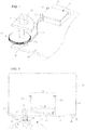
- the device comprises a driven element 10, a driving device 20 and a support 30.
- the support 30 comprises a flat receiving surface 31 on which the element to be driven 10 and the drive device 20 are arranged.
- the element to be driven 10 comprises a toothed wheel of generally cylindrical shape.
- the toothed wheel comprises a toothing composed of asymmetrical teeth 1, 2, 3, 4, 5 and a substantially cylindrical shaft 11.
- the support 30 comprises orifices 34, 35 of generally cylindrical shape, intended to receive the shaft 11.
- the orifices 34 and 35 form bearings capable of guiding the shaft 11 in rotation.
- the drive device 20 comprises a wafer 21 of semiconductor material, such as silicon.
- the drive device 20 comprises an actuator element 200, an indexing element 50 (not shown in the figure 1 ) and a drive element 250, formed by microgravure in the wafer 21.
- the drive element 250 is in the form of a tooth having a triangular shape.
- the tooth extends near the wheel 10 with the tip directed towards the wheel 10, in a radial direction relative to the wheel.
- the drive element 250 is thus able to mesh with the teeth 1, 2, 3, 4, 5 of the wheel 10.
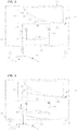
- the actuator element 200 mainly consists of an elementary tangential actuation module 202 and an indexing module 50.
- the tangential actuation module 202 comprises a structure with interdigitated combs 222 (known under the English name of "comb drive") and a flexible blade 212 extending in a general tangential direction relative to the wheel 10.
- L drive element 250 is connected by the tangential blade 212 to the interdigitated comb structure 222.
- the tangential actuation module 202 When the tangential actuation module 202 is controlled by an alternative addressing signal, the tangential actuation module 202 generates an alternating movement in a tangential direction (arrow I).
- the indexing module 50 comprises a flexible blade 511 extending in a tangential direction relative to the wheel 10 and an indexing element 550.
- the flexible blade 511 extends in cantilever from the substrate and is flexible in a radial direction relative to the wheel 10.
- the flexible blade 511 supports at its free end the indexing element 550.
- the indexing element 550 is in the form of a tooth having a triangular shape. The tooth extends near the wheel 10 with the tip directed towards the wheel 10, in a radial direction relative to the wheel. The indexing element 550 is thus able to be engaged with the teeth 1, 2, 3, 4, 5 of the wheel 10.
- the device also comprises two positioning pads 32 and 33 fixed on the support 30.
- the positioning pads 32 and 33 have a generally cylindrical shape and extend in a direction perpendicular to the receiving surface 31 of the support 30.
- the wafer 21 has two notches 22 and 23 formed on an outer edge 24 of the wafer.
- the notches 22 and 23 are arranged on either side of the drive element 250.
- the notch 22 is intended to receive the first positioning pad 32 and the notch 23 is intended to receive the second positioning pad 33 for positioning the plate 21 on the support 30.
- the positioning studs 32 and 33 define a unique position of the plate 21 on the receiving surface 31 of the support 30.
- the first notch 22 has a general V shape.
- the notch 22 has two bearing faces forming between them an angle of 120 °. Each bearing face of the first notch 22 is intended to come to bear on the cylindrical surface of the pad 32.
- the second notch 23 has a single bearing face, parallel to the edge 24 of the plate 21, intended to come to bear on the cylindrical surface of the pad 33.
- the positioning pads 32 and 33 cooperate with the notches 22 and 23 to define a position of the plate 20 on the receiving surface 31 of the support 30.
- the positioning pads 32 and 33 thus form reference pads which have the function of wedge the drive device parallel to the receiving surface 31.
- the assembly of the device comprises the following steps.
- the wheel 10 is rotatably mounted on the support 30.
- the shaft 11 is mounted on the bearings 34 and 35 so that the wheel 10 secured to the shaft 11 is able to rotate freely around an axis of rotation perpendicular to the receiving surface 31.
- the plate 21 is brought to bear on the first and second studs 32 and 33.
- the studs 32 and 33 are arranged on the support 30 so that the drive element 250 comes into contact with the wheel 10.
- the drive element 250 is kept in contact with the wheel 10 by means of the tangential blade 212.
- the blade 212 extends in overhang from the interdigitated comb structure 222 and is flexible in a radial direction relative to the wheel 10. Due to the elasticity of the blade 212, the drive element 250 is kept in engagement with the wheel 10.
- the flexible blade 212 absorbs the positioning faults of the plate 21 relative to the element to be driven 10.
- the device operates as follows.
- the tangential actuation module 202 is controlled by an alternative addressing signal.
- the drive element 250 engages the wheel 10 and pulls the wheel 10.
- the indexing element 550 crosses a tooth of wheel 10.
- the indexing element 550 blocks the wheel 10 and the drive element 250 slides on the wheel 10.
- the wheel 10 is thus driven in a stepwise rotation movement (arrow III) by the drive element 250.
- the indexing element 50 forms a non-return pawl which prevents the rotation of the wheel 10 in the direction reverse.
- the figures 3 and 4 represent a device according to a second embodiment of the invention.
- the assembly is identical to the assembly of the first embodiment, except that the actuator element 200 comprises a radial actuation module 203.
- the device comprises a driven element 10, a driving device 20 and a support 30.
- the element to be driven 10 comprises a wheel, possibly toothed.
- the drive device 20 comprises a wafer 21 of semiconductor material, such as silicon.
- the drive device 20 comprises an actuator element 200 and a drive element 250 formed by microgravure in the wafer 21.
- the actuator element 200 mainly consists of an elementary tangential actuation module 202 and an elementary radial actuation module 203,
- the tangential actuation module 202 comprises a structure with interdigitated combs 222 and a flexible blade 212 extending in a general tangential direction relative to the wheel 10.
- the drive element 250 is connected by the tangential blade 212 to the interdigitated comb structure 222.
- the tangential actuation module 202 When the tangential actuation module 202 is controlled by an alternative addressing signal, the tangential actuation module 202 generates an alternating movement in a tangential direction (arrow I).
- the radial actuation module 203 comprises an electrode 223, a flexible blade 210 and stops 243.
- the flexible blade 210 has a general shape of L and comprises a first branch 213 and a second branch 214.
- the first branch 213 extends in a tangential direction with respect to the wheel 10.
- the first branch 213 extends in cantilever from the substrate and is flexible in a radial direction with respect to the wheel 10.
- the second branch 214 extends in a generally radial direction relative to the wheel and connects the free end of the first branch 213 to the drive element 250.
- the electrode 223 is shown in more detail on the figure 5 .
- the electrode 223 has a lateral surface 233 of generally convex shape, preferably parabolic.
- the stops 243 are arranged at regular intervals along the lateral surface 233.
- the stops 243 are formed by studs etched in the wafer 21. The studs are electrically isolated from the electrode 223.
- the stops 243 limit the amplitude of movement of the blade 210 to keep the blade 210 away from the electrode 223 and prevent the first branch 213 from coming into contact with the lateral surface 233 of the electrode 223. In effect, the contact of blade 210 and the electrode 223 supplied at different voltages would cause a short circuit which could cause the device to fail.
- the convex shape of the surface 233 of the electrode makes it possible to control the movement of the rod 210 whatever the initial deformation of the branch 213 due to the positioning of the drive tooth 250 relative to the wheel 10.
- the branch 213 of the blade 210 thus absorbs the uncertainties of positioning the wafer relative to the wheel 10.
- the tangential actuation module 202 When the tangential actuation module 202 is controlled by an alternative addressing signal, the tangential actuation module 202 generates an alternating movement in a tangential direction (arrow I) relative to the wheel 10.
- the radial actuation module 203 When the electrode 223 of the radial actuation module 203 is controlled by an alternating addressing signal, the radial actuation module 203 generates an alternating movement in a radial direction (arrow II) relative to the wheel 10.
- the device operates as follows.
- the tangential actuation module 202 and the radial actuation module 203 are controlled by alternative addressing signals.
- the addressing signals are out of phase so that the drive element 250 is moved in a hysteresis movement.
- the hysteresis movement of the drive tooth 250 alternates the drive (arrow I) and actuation (arrow II) phases.
- the drive element 250 meshes with the successive teeth of the wheel 10 and drives the latter in a stepwise rotation movement.
- each of the blades 212 and 210 allows the deformation of the latter under the action of the other blade.
- the two flexible radial and tangential blades 212 and 214 provide mechanical decoupling of the modules 202 and 203.
- the flexibility of the blades allows the drive element 250 to be displaced independently according to two elementary degrees of freedom, namely: according to the two directions of radial and tangential translation.
Landscapes
- Micromachines (AREA)
- Transmission Devices (AREA)
Claims (13)
- MEMS-Vorrichtung mit einem anzutreibenden Element (10), einem Antriebselement (250), das dafür vorgesehen ist, mit dem anzutreibenden Element (10) in Eingriff zu kommen, und einem Betätigungselement (200), welches das Antriebselement (250) derart bewegen kann, dass es das anzutreibende Element (10) in einer schrittweisen Bewegung antreibt, wobei das Antriebselement (250) und das Betätigungselement (200) in einem Plättchen (21) aus Halbleitermaterial ausgebildet sind, wobei die Vorrichtung auch einen Träger (30) umfasst, auf dem das Plättchen (21) und das anzutreibende Element (10) angeordnet sind, wobei das anzutreibende Element (10) drehbar auf dem Träger (30) montiert ist,
dadurch gekennzeichnet, dass das Betätigungselement (200) durch Ätzen in dem Plättchen (21) gebildet wird und das anzutreibende Element (10) durch eine andere Technologie als die Mikroätzung realisiert wird, wobei die Vorrichtung Mittel zur elastischen Vorspannung (212) umfasst, um das Antriebselement (250) in Kontakt mit dem anzutreibenden Element (10) zu halten. - Vorrichtung nach Anspruch 1, wobei sich die Mittel zur elastischen Vorspannung (212) zwischen dem Betätigungselement (200) und dem Antriebselement (250) erstrecken.
- Vorrichtung nach einem der vorstehenden Ansprüche, wobei die Mittel zur elastischen Vorspannung (212) eine flexible Lamelle (212) umfassen, die das Antriebselement (250) mit dem Betätigungselement (200) verbindet.
- Vorrichtung nach Anspruch 1 umfassend Positionierungsstifte (32, 33), die auf dem Träger (30) befestigt sind, zum Positionieren des Plättchens (21) auf dem Träger (30).
- Vorrichtung nach Anspruch 4, wobei das Plättchen (21) auf den Positionierungsstiften (32, 33) aufliegend angeordnet ist.
- Vorrichtung nach Anspruch 5, wobei das Plättchen (21) mindestens eine Kerbe (22, 23) aufweist, die an einem Rand (24) des Plättchens (21) ausgebildet ist, wobei die Kerbe (22, 23) dafür vorgesehen ist, einen Positionierungsstift (32, 33) aufzunehmen, um das Plättchen (21) auf dem Träger (30) zu positionieren.
- Vorrichtung nach einem der vorstehenden Ansprüche, wobei das Betätigungselement (200) ein erstes Betätigungsmodul (202) umfasst, welches das Antriebselement (250) in einer ersten Richtung bewegen kann, um das anzutreibende Element (10) anzutreiben, und ein zweites Betätigungsmodul (203) umfasst, welches das Antriebselement (250) in einer zweiten Richtung bewegen kann, um das Antriebselement (250) von dem anzutreibenden Element (10) weg zu bewegen, wobei die Betätigungsmodule (202, 203) gleichzeitig gesteuert werden können, um eine kombinierte Hysteresebewegung des Antriebselements (250) zu erzeugen.
- Vorrichtung nach Anspruch 7, wobei das zweite Betätigungsmodul (203) eine Elektrode (223) und eine flexible Stange (210) umfasst, wobei die Elektrode dahingehend gesteuert werden kann, die flexible Stange (210) derart zu verformen, dass das Antriebselement (250) in einer zweiten Richtung bewegt wird, um das Antriebselement (250) von dem anzutreibenden Element (10) weg zu bewegen.
- Vorrichtung nach Anspruch 8, wobei die Elektrode eine konvexe, vorzugsweise parabolische Seitenfläche (233) aufweist, die sich gegenüber einem Abschnitt (213) der flexiblen Lamelle (210) erstreckt.
- Vorrichtung nach einem der Ansprüche 8 oder 9, wobei das zweite Betätigungsmodul (203) eine Reihe von Anschlägen (243) umfasst, die entlang einer Seitenfläche (233) der Elektrode (223) angeordnet sind, wobei die Anschläge (243) den Kontakt zwischen der Lamelle (210) und der Elektrode (223) verhindern können.
- Montageverfahren für eine Vorrichtung nach einem der Ansprüche 1 bis 10, wobei das Verfahren die Schritte umfasst:i) Ätzen in ein Plättchen (21) aus Halbleitermaterial eines Antriebselements (250), das dafür vorgesehen ist, mit einem anzutreibenden Element (10) in Eingriff zu kommen, und eines Betätigungselements (200), welches das Antriebselement (250) bewegen kann,ii) Anordnen auf demselben Träger (30):- des drehend anzutreibenden Elements (10) auf dem Träger (30), wobei das anzutreibende Element (10) durch eine andere Technologie als Mikroätzen realisiert wird, und- des Plättchens (21), eines Betätigungselements (200), welches das Antriebselement (250) derart bewegen kann, dass es das anzutreibende Element (10) in einer schrittweisen Bewegung in Bezug auf den Träger (30) antreibt,iii) Herstellen des Kontakts zwischen dem Antriebselement (250) und dem anzutreibenden Element (10) mittels der Mittel zur elastischen Vorspannung (210, 212).
- Verfahren nach Anspruch 11, wobei die Vorrichtung Positionierungsstifte (32, 33) umfasst, die auf dem Träger (30) befestigt sind, wobei das Verfahren den Schritt umfasst:- Anordnen des Plättchens (21) aufliegend auf den Positionierungsstiften (32, 33).
- Verfahren nach Anspruch 12, wobei das Plättchen (21) mindestens eine Kerbe (22, 23) aufweist, die an einem Rand (24) des Plättchens (21) ausgebildet ist, wobei das Verfahren den Schritt umfasst:- Anordnen eines Positionierungsstiftes (32, 33) in der Kerbe (22, 23) zum Positionieren des Plättchens (21) auf dem Träger (30).
Applications Claiming Priority (2)
| Application Number | Priority Date | Filing Date | Title |
|---|---|---|---|
| FR0502700A FR2883277B1 (fr) | 2005-03-18 | 2005-03-18 | Procede et dispositif pour deplacer un element a entrainer utilisant un element actionneur forme par gravure dans un materiau semi-conducteur |
| PCT/EP2006/060806 WO2006097516A1 (fr) | 2005-03-18 | 2006-03-16 | Procede et dispositif pour deplacer un element a entrainer utilisant un element actionneur forme par gravure dans un materiau semi-conducteur |
Publications (2)
| Publication Number | Publication Date |
|---|---|
| EP1864374A1 EP1864374A1 (de) | 2007-12-12 |
| EP1864374B1 true EP1864374B1 (de) | 2020-04-22 |
Family
ID=35148972
Family Applications (1)
| Application Number | Title | Priority Date | Filing Date |
|---|---|---|---|
| EP06725112.4A Expired - Lifetime EP1864374B1 (de) | 2005-03-18 | 2006-03-16 | Einrichtung und verfahren zur verstellung einer antrieb, mit aktuatorelement in halbleitermaterial geätzten |
Country Status (6)
| Country | Link |
|---|---|
| US (1) | US8058772B2 (de) |
| EP (1) | EP1864374B1 (de) |
| JP (1) | JP2009529429A (de) |
| ES (1) | ES2791678T3 (de) |
| FR (1) | FR2883277B1 (de) |
| WO (1) | WO2006097516A1 (de) |
Families Citing this family (6)
| Publication number | Priority date | Publication date | Assignee | Title |
|---|---|---|---|---|
| DE602006005058D1 (de) | 2006-11-13 | 2009-03-19 | Eta Sa Mft Horlogere Suisse | Einen MEMS-Mikromotor umfassendes Antriebsmodul, Verfahren zur Herstellung dieses Moduls und mit diesem Modul ausgerüstete Uhr |
| DE602006019612D1 (de) | 2006-11-13 | 2011-02-24 | Eta Sa Mft Horlogere Suisse | MEMS-Mikromotor und mit diesem Mikromotor ausgerüstete Uhr |
| ATE475119T1 (de) | 2006-11-13 | 2010-08-15 | Eta Sa Mft Horlogere Suisse | Anordnung zur mechanischen verbindung eines mems- mikromotors mit einem uhrrädchen und diese anordnung umfassende uhr |
| EP2177960B1 (de) * | 2008-10-16 | 2011-12-21 | ETA SA Manufacture Horlogère Suisse | Blockiermechanismus für Modul eines Uhrwerksantriebs |
| FR2985721B1 (fr) * | 2012-01-12 | 2017-04-07 | Silmach | Indexation passive d'un element mobile presentant des dents |
| US8926465B2 (en) * | 2013-01-07 | 2015-01-06 | Timex Group Usa, Inc. | Bidirectional MEMS driving arrangement |
Citations (2)
| Publication number | Priority date | Publication date | Assignee | Title |
|---|---|---|---|---|
| WO2001009519A1 (en) * | 1999-07-30 | 2001-02-08 | The Procter & Gamble Company | Microvalve for controlling fluid flow |
| US6313562B1 (en) * | 1999-08-03 | 2001-11-06 | Sandia Corporation | Microelectromechanical ratcheting apparatus |
Family Cites Families (18)
| Publication number | Priority date | Publication date | Assignee | Title |
|---|---|---|---|---|
| US3465805A (en) * | 1968-03-29 | 1969-09-09 | Hugh M Lyman | Drive means for partitions and the like |
| JPS5057475A (de) * | 1973-09-13 | 1975-05-19 | ||
| JPS5226933Y1 (de) * | 1974-05-13 | 1977-06-18 | ||
| JPS5226933A (en) * | 1975-08-21 | 1977-02-28 | Yoshio Wakana | Pin ball game achine |
| JPS58149102U (ja) * | 1982-03-29 | 1983-10-06 | 株式会社吉野工業所 | 化粧用コンパクト容器 |
| US6211111B1 (en) * | 1998-08-17 | 2001-04-03 | The Dow Chemical Company | Activator composition comprising aluminum compound mixture |
| US6354922B1 (en) * | 1999-08-20 | 2002-03-12 | Ebara Corporation | Polishing apparatus |
| US6887615B1 (en) * | 1999-07-30 | 2005-05-03 | The Procter & Gamble Company | Microvalve for controlling fluid flow |
| JP4066298B2 (ja) * | 2000-03-23 | 2008-03-26 | 三井住友建設株式会社 | 緩衝材挿入型継手 |
| US6465929B1 (en) * | 2000-04-07 | 2002-10-15 | Microsoft Corporation | Microelectromechanical system actuator for extended linear motion |
| FR2809549B1 (fr) * | 2000-05-25 | 2003-06-27 | Centre Nat Rech Scient | Dispositif formant micromoteur ou microactionneur |
| US6646364B1 (en) * | 2000-07-11 | 2003-11-11 | Honeywell International Inc. | MEMS actuator with lower power consumption and lower cost simplified fabrication |
| JP3680992B2 (ja) * | 2001-05-11 | 2005-08-10 | 大日本スクリーン製造株式会社 | 円筒外面走査装置 |
| US6729856B2 (en) * | 2001-10-09 | 2004-05-04 | Honeywell International Inc. | Electrostatically actuated pump with elastic restoring forces |
| JP4307813B2 (ja) * | 2001-11-14 | 2009-08-05 | 株式会社リコー | 光偏向方法並びに光偏向装置及びその光偏向装置の製造方法並びにその光偏向装置を具備する光情報処理装置及び画像形成装置及び画像投影表示装置及び光伝送装置 |
| JP2003145810A (ja) * | 2001-11-16 | 2003-05-21 | Hitachi Printing Solutions Ltd | ドットプリンタ及びそれに用いる印字ユニット交換冶具 |
| FR2852111B1 (fr) * | 2003-03-05 | 2005-06-24 | Univ Franche Comte | Dispositif d'horloge utilisant la technologie mems |
| JP4467367B2 (ja) * | 2004-06-22 | 2010-05-26 | 大日本スクリーン製造株式会社 | 基板反転装置、基板搬送装置、基板処理装置、基板反転方法、基板搬送方法および基板処理方法 |
-
2005
- 2005-03-18 FR FR0502700A patent/FR2883277B1/fr not_active Expired - Fee Related
-
2006
- 2006-03-16 ES ES06725112T patent/ES2791678T3/es not_active Expired - Lifetime
- 2006-03-16 JP JP2008501323A patent/JP2009529429A/ja active Pending
- 2006-03-16 WO PCT/EP2006/060806 patent/WO2006097516A1/fr not_active Ceased
- 2006-03-16 EP EP06725112.4A patent/EP1864374B1/de not_active Expired - Lifetime
- 2006-03-16 US US11/886,504 patent/US8058772B2/en active Active
Patent Citations (2)
| Publication number | Priority date | Publication date | Assignee | Title |
|---|---|---|---|---|
| WO2001009519A1 (en) * | 1999-07-30 | 2001-02-08 | The Procter & Gamble Company | Microvalve for controlling fluid flow |
| US6313562B1 (en) * | 1999-08-03 | 2001-11-06 | Sandia Corporation | Microelectromechanical ratcheting apparatus |
Also Published As
| Publication number | Publication date |
|---|---|
| WO2006097516A8 (fr) | 2007-11-08 |
| FR2883277A1 (fr) | 2006-09-22 |
| US8058772B2 (en) | 2011-11-15 |
| ES2791678T3 (es) | 2020-11-05 |
| US20090096323A1 (en) | 2009-04-16 |
| JP2009529429A (ja) | 2009-08-20 |
| EP1864374A1 (de) | 2007-12-12 |
| WO2006097516A1 (fr) | 2006-09-21 |
| FR2883277B1 (fr) | 2007-05-11 |
Similar Documents
| Publication | Publication Date | Title |
|---|---|---|
| EP3559755B1 (de) | Flexible monolithisches bauteil für uhren | |
| EP2135305B1 (de) | Feineinstellungssystem mit trägheitsmotor auf der basis eines mechanischen verstärkers | |
| EP1921521B1 (de) | MEMS-Mikromotor und mit diesem Mikromotor ausgerüstete Uhr | |
| EP1797483B1 (de) | Antriebseinrichtung insbesondere für ein uhrwerk | |
| EP1599766B1 (de) | Herstellungsverfahren einer mems einrichtung | |
| EP2927756A1 (de) | Uhrwerk, das mit einem Antriebsmechanismus eines Analoganzeigers mit periodischer oder intermittierender Bewegung ausgestattet ist | |
| EP1864374B1 (de) | Einrichtung und verfahren zur verstellung einer antrieb, mit aktuatorelement in halbleitermaterial geätzten | |
| EP2781009A1 (de) | Anzeigemodul für ein armaturenbrett mit flüssigkeitsbewegung | |
| EP1921518B1 (de) | Montageelement, das dehnbare Strukturen in Form von aufeinander liegenden Plättchen umfasst, und mit diesem Element ausgerüstete Uhr | |
| EP2736161B1 (de) | Betätigungsvorrichtung mit durch Kriechbewegung ausgelöstem Antriebselement | |
| EP1921522B1 (de) | Anordnung zur mechanischen Verbindung eines MEMS-Mikromotors mit einem Uhrrädchen und diese Anordnung umfassende Uhr | |
| EP0580049A1 (de) | Piezo-elektrischer Motor | |
| EP1878108B1 (de) | Einrichtung und verfahren zur verstellung einer antrieb, mit aktuatorelement in halbleitermaterial geätzten | |
| EP3037893B1 (de) | Mikromechanische Komponente oder Uhr mit flexiblem Führungsdraht | |
| CH714165B1 (fr) | Dispositif pour pièce d'horlogerie, mouvement horloger et pièce d'horlogerie comprenant un tel dispositif. | |
| EP4341753B1 (de) | Mikroelektromechanisches system zum bewegen eines mechanischen teils in zwei entgegengesetzte richtungen | |
| EP2735922A1 (de) | Zeigerantriebsmechanismus einer elektromechanischen Armbanduhr, der mit einer Verriegelung ausgestattet ist | |
| CH714767B1 (fr) | Dispositif de collecte d'énergie mécanique notamment pour pièce d'horlogerie, mouvement horloger et pièce d'horlogerie comprenant un tel dispositif. | |
| EP3851919B1 (de) | Repositionierungsvorrichtung für uhrwerk | |
| EP4341203A1 (de) | Verfahren zur steuerung eines mikroelektromechanischen systems | |
| CH680252B5 (de) | ||
| EP1965277B1 (de) | Anker für Uhrhemmungsmechanismus vom Typ Anker und Rad | |
| WO2002086584A1 (fr) | Commutateur optique multivoie | |
| WO2022243645A1 (fr) | Microsysteme electromecanique permettant de deplacer une piece mecanique selon deux sens opposes | |
| EP1746071A1 (de) | Mikroaktuator mit Balken mit gekrümmten Segmenten |
Legal Events
| Date | Code | Title | Description |
|---|---|---|---|
| PUAI | Public reference made under article 153(3) epc to a published international application that has entered the european phase |
Free format text: ORIGINAL CODE: 0009012 |
|
| 17P | Request for examination filed |
Effective date: 20071009 |
|
| AK | Designated contracting states |
Kind code of ref document: A1 Designated state(s): CH DE ES GB IT LI NL |
|
| DAX | Request for extension of the european patent (deleted) | ||
| RBV | Designated contracting states (corrected) |
Designated state(s): CH DE ES GB IT LI NL |
|
| RAP1 | Party data changed (applicant data changed or rights of an application transferred) |
Owner name: SILMACH |
|
| 17Q | First examination report despatched |
Effective date: 20160804 |
|
| GRAP | Despatch of communication of intention to grant a patent |
Free format text: ORIGINAL CODE: EPIDOSNIGR1 |
|
| INTG | Intention to grant announced |
Effective date: 20191111 |
|
| GRAS | Grant fee paid |
Free format text: ORIGINAL CODE: EPIDOSNIGR3 |
|
| GRAA | (expected) grant |
Free format text: ORIGINAL CODE: 0009210 |
|
| STAA | Information on the status of an ep patent application or granted ep patent |
Free format text: STATUS: THE PATENT HAS BEEN GRANTED |
|
| AK | Designated contracting states |
Kind code of ref document: B1 Designated state(s): CH DE ES GB IT LI NL |
|
| REG | Reference to a national code |
Ref country code: GB Ref legal event code: FG4D Free format text: NOT ENGLISH |
|
| REG | Reference to a national code |
Ref country code: CH Ref legal event code: EP |
|
| REG | Reference to a national code |
Ref country code: DE Ref legal event code: R096 Ref document number: 602006059341 Country of ref document: DE |
|
| REG | Reference to a national code |
Ref country code: CH Ref legal event code: NV Representative=s name: MICHELI AND CIE SA, CH |
|
| REG | Reference to a national code |
Ref country code: NL Ref legal event code: FP |
|
| REG | Reference to a national code |
Ref country code: ES Ref legal event code: FG2A Ref document number: 2791678 Country of ref document: ES Kind code of ref document: T3 Effective date: 20201105 |
|
| REG | Reference to a national code |
Ref country code: DE Ref legal event code: R097 Ref document number: 602006059341 Country of ref document: DE |
|
| PLBE | No opposition filed within time limit |
Free format text: ORIGINAL CODE: 0009261 |
|
| STAA | Information on the status of an ep patent application or granted ep patent |
Free format text: STATUS: NO OPPOSITION FILED WITHIN TIME LIMIT |
|
| 26N | No opposition filed |
Effective date: 20210125 |
|
| PGFP | Annual fee paid to national office [announced via postgrant information from national office to epo] |
Ref country code: NL Payment date: 20230227 Year of fee payment: 18 |
|
| PGFP | Annual fee paid to national office [announced via postgrant information from national office to epo] |
Ref country code: IT Payment date: 20230309 Year of fee payment: 18 Ref country code: GB Payment date: 20230324 Year of fee payment: 18 Ref country code: DE Payment date: 20230307 Year of fee payment: 18 |
|
| PGFP | Annual fee paid to national office [announced via postgrant information from national office to epo] |
Ref country code: ES Payment date: 20230405 Year of fee payment: 18 Ref country code: CH Payment date: 20230402 Year of fee payment: 18 |
|
| REG | Reference to a national code |
Ref country code: DE Ref legal event code: R119 Ref document number: 602006059341 Country of ref document: DE |
|
| REG | Reference to a national code |
Ref country code: CH Ref legal event code: PL |
|
| REG | Reference to a national code |
Ref country code: NL Ref legal event code: MM Effective date: 20240401 |
|
| GBPC | Gb: european patent ceased through non-payment of renewal fee |
Effective date: 20240316 |
|
| PG25 | Lapsed in a contracting state [announced via postgrant information from national office to epo] |
Ref country code: NL Free format text: LAPSE BECAUSE OF NON-PAYMENT OF DUE FEES Effective date: 20240401 |
|
| PG25 | Lapsed in a contracting state [announced via postgrant information from national office to epo] |
Ref country code: NL Free format text: LAPSE BECAUSE OF NON-PAYMENT OF DUE FEES Effective date: 20240401 |
|
| PG25 | Lapsed in a contracting state [announced via postgrant information from national office to epo] |
Ref country code: DE Free format text: LAPSE BECAUSE OF NON-PAYMENT OF DUE FEES Effective date: 20241001 |
|
| PG25 | Lapsed in a contracting state [announced via postgrant information from national office to epo] |
Ref country code: GB Free format text: LAPSE BECAUSE OF NON-PAYMENT OF DUE FEES Effective date: 20240316 |
|
| PG25 | Lapsed in a contracting state [announced via postgrant information from national office to epo] |
Ref country code: GB Free format text: LAPSE BECAUSE OF NON-PAYMENT OF DUE FEES Effective date: 20240316 Ref country code: DE Free format text: LAPSE BECAUSE OF NON-PAYMENT OF DUE FEES Effective date: 20241001 Ref country code: CH Free format text: LAPSE BECAUSE OF NON-PAYMENT OF DUE FEES Effective date: 20240331 |
|
| PG25 | Lapsed in a contracting state [announced via postgrant information from national office to epo] |
Ref country code: IT Free format text: LAPSE BECAUSE OF NON-PAYMENT OF DUE FEES Effective date: 20240316 |
|
| REG | Reference to a national code |
Ref country code: ES Ref legal event code: FD2A Effective date: 20250429 |
|
| PG25 | Lapsed in a contracting state [announced via postgrant information from national office to epo] |
Ref country code: ES Free format text: LAPSE BECAUSE OF NON-PAYMENT OF DUE FEES Effective date: 20240317 |